US4659422A - Process for producing monocrystalline layer on insulator - Google Patents
Process for producing monocrystalline layer on insulator Download PDFInfo
- Publication number
- US4659422A US4659422A US06/592,067 US59206784A US4659422A US 4659422 A US4659422 A US 4659422A US 59206784 A US59206784 A US 59206784A US 4659422 A US4659422 A US 4659422A
- Authority
- US
- United States
- Prior art keywords
- layer
- nonmonocrystalline
- lamps
- process according
- heat sources
- Prior art date
- Legal status (The legal status is an assumption and is not a legal conclusion. Google has not performed a legal analysis and makes no representation as to the accuracy of the status listed.)
- Expired - Fee Related
Links
Images


Classifications
-
- H—ELECTRICITY
- H01—ELECTRIC ELEMENTS
- H01L—SEMICONDUCTOR DEVICES NOT COVERED BY CLASS H10
- H01L21/00—Processes or apparatus adapted for the manufacture or treatment of semiconductor or solid state devices or of parts thereof
- H01L21/02—Manufacture or treatment of semiconductor devices or of parts thereof
- H01L21/02104—Forming layers
- H01L21/02365—Forming inorganic semiconducting materials on a substrate
- H01L21/02656—Special treatments
- H01L21/02664—Aftertreatments
- H01L21/02667—Crystallisation or recrystallisation of non-monocrystalline semiconductor materials, e.g. regrowth
-
- C—CHEMISTRY; METALLURGY
- C30—CRYSTAL GROWTH
- C30B—SINGLE-CRYSTAL GROWTH; UNIDIRECTIONAL SOLIDIFICATION OF EUTECTIC MATERIAL OR UNIDIRECTIONAL DEMIXING OF EUTECTOID MATERIAL; REFINING BY ZONE-MELTING OF MATERIAL; PRODUCTION OF A HOMOGENEOUS POLYCRYSTALLINE MATERIAL WITH DEFINED STRUCTURE; SINGLE CRYSTALS OR HOMOGENEOUS POLYCRYSTALLINE MATERIAL WITH DEFINED STRUCTURE; AFTER-TREATMENT OF SINGLE CRYSTALS OR A HOMOGENEOUS POLYCRYSTALLINE MATERIAL WITH DEFINED STRUCTURE; APPARATUS THEREFOR
- C30B13/00—Single-crystal growth by zone-melting; Refining by zone-melting
- C30B13/16—Heating of the molten zone
- C30B13/22—Heating of the molten zone by irradiation or electric discharge
- C30B13/24—Heating of the molten zone by irradiation or electric discharge using electromagnetic waves
-
- C—CHEMISTRY; METALLURGY
- C30—CRYSTAL GROWTH
- C30B—SINGLE-CRYSTAL GROWTH; UNIDIRECTIONAL SOLIDIFICATION OF EUTECTIC MATERIAL OR UNIDIRECTIONAL DEMIXING OF EUTECTOID MATERIAL; REFINING BY ZONE-MELTING OF MATERIAL; PRODUCTION OF A HOMOGENEOUS POLYCRYSTALLINE MATERIAL WITH DEFINED STRUCTURE; SINGLE CRYSTALS OR HOMOGENEOUS POLYCRYSTALLINE MATERIAL WITH DEFINED STRUCTURE; AFTER-TREATMENT OF SINGLE CRYSTALS OR A HOMOGENEOUS POLYCRYSTALLINE MATERIAL WITH DEFINED STRUCTURE; APPARATUS THEREFOR
- C30B29/00—Single crystals or homogeneous polycrystalline material with defined structure characterised by the material or by their shape
- C30B29/60—Single crystals or homogeneous polycrystalline material with defined structure characterised by the material or by their shape characterised by shape
-
- H—ELECTRICITY
- H01—ELECTRIC ELEMENTS
- H01L—SEMICONDUCTOR DEVICES NOT COVERED BY CLASS H10
- H01L21/00—Processes or apparatus adapted for the manufacture or treatment of semiconductor or solid state devices or of parts thereof
- H01L21/02—Manufacture or treatment of semiconductor devices or of parts thereof
- H01L21/02104—Forming layers
- H01L21/02365—Forming inorganic semiconducting materials on a substrate
- H01L21/02367—Substrates
- H01L21/0237—Materials
- H01L21/02373—Group 14 semiconducting materials
- H01L21/02381—Silicon, silicon germanium, germanium
-
- H—ELECTRICITY
- H01—ELECTRIC ELEMENTS
- H01L—SEMICONDUCTOR DEVICES NOT COVERED BY CLASS H10
- H01L21/00—Processes or apparatus adapted for the manufacture or treatment of semiconductor or solid state devices or of parts thereof
- H01L21/02—Manufacture or treatment of semiconductor devices or of parts thereof
- H01L21/02104—Forming layers
- H01L21/02365—Forming inorganic semiconducting materials on a substrate
- H01L21/02367—Substrates
- H01L21/02433—Crystal orientation
-
- H—ELECTRICITY
- H01—ELECTRIC ELEMENTS
- H01L—SEMICONDUCTOR DEVICES NOT COVERED BY CLASS H10
- H01L21/00—Processes or apparatus adapted for the manufacture or treatment of semiconductor or solid state devices or of parts thereof
- H01L21/02—Manufacture or treatment of semiconductor devices or of parts thereof
- H01L21/02104—Forming layers
- H01L21/02365—Forming inorganic semiconducting materials on a substrate
- H01L21/02436—Intermediate layers between substrates and deposited layers
- H01L21/02439—Materials
- H01L21/02488—Insulating materials
-
- H—ELECTRICITY
- H01—ELECTRIC ELEMENTS
- H01L—SEMICONDUCTOR DEVICES NOT COVERED BY CLASS H10
- H01L21/00—Processes or apparatus adapted for the manufacture or treatment of semiconductor or solid state devices or of parts thereof
- H01L21/02—Manufacture or treatment of semiconductor devices or of parts thereof
- H01L21/02104—Forming layers
- H01L21/02365—Forming inorganic semiconducting materials on a substrate
- H01L21/02436—Intermediate layers between substrates and deposited layers
- H01L21/02494—Structure
- H01L21/02496—Layer structure
- H01L21/02505—Layer structure consisting of more than two layers
-
- H—ELECTRICITY
- H01—ELECTRIC ELEMENTS
- H01L—SEMICONDUCTOR DEVICES NOT COVERED BY CLASS H10
- H01L21/00—Processes or apparatus adapted for the manufacture or treatment of semiconductor or solid state devices or of parts thereof
- H01L21/02—Manufacture or treatment of semiconductor devices or of parts thereof
- H01L21/02104—Forming layers
- H01L21/02365—Forming inorganic semiconducting materials on a substrate
- H01L21/02518—Deposited layers
- H01L21/02521—Materials
- H01L21/02524—Group 14 semiconducting materials
- H01L21/02532—Silicon, silicon germanium, germanium
-
- H—ELECTRICITY
- H01—ELECTRIC ELEMENTS
- H01L—SEMICONDUCTOR DEVICES NOT COVERED BY CLASS H10
- H01L21/00—Processes or apparatus adapted for the manufacture or treatment of semiconductor or solid state devices or of parts thereof
- H01L21/02—Manufacture or treatment of semiconductor devices or of parts thereof
- H01L21/02104—Forming layers
- H01L21/02365—Forming inorganic semiconducting materials on a substrate
- H01L21/02518—Deposited layers
- H01L21/02587—Structure
- H01L21/0259—Microstructure
- H01L21/02598—Microstructure monocrystalline
-
- H—ELECTRICITY
- H01—ELECTRIC ELEMENTS
- H01L—SEMICONDUCTOR DEVICES NOT COVERED BY CLASS H10
- H01L21/00—Processes or apparatus adapted for the manufacture or treatment of semiconductor or solid state devices or of parts thereof
- H01L21/02—Manufacture or treatment of semiconductor devices or of parts thereof
- H01L21/02104—Forming layers
- H01L21/02365—Forming inorganic semiconducting materials on a substrate
- H01L21/02656—Special treatments
- H01L21/02664—Aftertreatments
- H01L21/02667—Crystallisation or recrystallisation of non-monocrystalline semiconductor materials, e.g. regrowth
- H01L21/02691—Scanning of a beam
-
- H—ELECTRICITY
- H01—ELECTRIC ELEMENTS
- H01L—SEMICONDUCTOR DEVICES NOT COVERED BY CLASS H10
- H01L21/00—Processes or apparatus adapted for the manufacture or treatment of semiconductor or solid state devices or of parts thereof
- H01L21/02—Manufacture or treatment of semiconductor devices or of parts thereof
- H01L21/04—Manufacture or treatment of semiconductor devices or of parts thereof the devices having at least one potential-jump barrier or surface barrier, e.g. PN junction, depletion layer or carrier concentration layer
- H01L21/18—Manufacture or treatment of semiconductor devices or of parts thereof the devices having at least one potential-jump barrier or surface barrier, e.g. PN junction, depletion layer or carrier concentration layer the devices having semiconductor bodies comprising elements of Group IV of the Periodic System or AIIIBV compounds with or without impurities, e.g. doping materials
- H01L21/26—Bombardment with radiation
- H01L21/263—Bombardment with radiation with high-energy radiation
- H01L21/268—Bombardment with radiation with high-energy radiation using electromagnetic radiation, e.g. laser radiation
- H01L21/2686—Bombardment with radiation with high-energy radiation using electromagnetic radiation, e.g. laser radiation using incoherent radiation
-
- H—ELECTRICITY
- H01—ELECTRIC ELEMENTS
- H01L—SEMICONDUCTOR DEVICES NOT COVERED BY CLASS H10
- H01L21/00—Processes or apparatus adapted for the manufacture or treatment of semiconductor or solid state devices or of parts thereof
- H01L21/02—Manufacture or treatment of semiconductor devices or of parts thereof
- H01L21/04—Manufacture or treatment of semiconductor devices or of parts thereof the devices having at least one potential-jump barrier or surface barrier, e.g. PN junction, depletion layer or carrier concentration layer
- H01L21/18—Manufacture or treatment of semiconductor devices or of parts thereof the devices having at least one potential-jump barrier or surface barrier, e.g. PN junction, depletion layer or carrier concentration layer the devices having semiconductor bodies comprising elements of Group IV of the Periodic System or AIIIBV compounds with or without impurities, e.g. doping materials
- H01L21/30—Treatment of semiconductor bodies using processes or apparatus not provided for in groups H01L21/20 - H01L21/26
- H01L21/324—Thermal treatment for modifying the properties of semiconductor bodies, e.g. annealing, sintering
-
- Y—GENERAL TAGGING OF NEW TECHNOLOGICAL DEVELOPMENTS; GENERAL TAGGING OF CROSS-SECTIONAL TECHNOLOGIES SPANNING OVER SEVERAL SECTIONS OF THE IPC; TECHNICAL SUBJECTS COVERED BY FORMER USPC CROSS-REFERENCE ART COLLECTIONS [XRACs] AND DIGESTS
- Y10—TECHNICAL SUBJECTS COVERED BY FORMER USPC
- Y10T—TECHNICAL SUBJECTS COVERED BY FORMER US CLASSIFICATION
- Y10T117/00—Single-crystal, oriented-crystal, and epitaxy growth processes; non-coating apparatus therefor
- Y10T117/10—Apparatus
- Y10T117/1024—Apparatus for crystallization from liquid or supercritical state
- Y10T117/1076—Apparatus for crystallization from liquid or supercritical state having means for producing a moving solid-liquid-solid zone
- Y10T117/108—Including a solid member other than seed or product contacting the liquid [e.g., crucible, immersed heating element]
-
- Y—GENERAL TAGGING OF NEW TECHNOLOGICAL DEVELOPMENTS; GENERAL TAGGING OF CROSS-SECTIONAL TECHNOLOGIES SPANNING OVER SEVERAL SECTIONS OF THE IPC; TECHNICAL SUBJECTS COVERED BY FORMER USPC CROSS-REFERENCE ART COLLECTIONS [XRACs] AND DIGESTS
- Y10—TECHNICAL SUBJECTS COVERED BY FORMER USPC
- Y10T—TECHNICAL SUBJECTS COVERED BY FORMER US CLASSIFICATION
- Y10T117/00—Single-crystal, oriented-crystal, and epitaxy growth processes; non-coating apparatus therefor
- Y10T117/10—Apparatus
- Y10T117/1024—Apparatus for crystallization from liquid or supercritical state
- Y10T117/1076—Apparatus for crystallization from liquid or supercritical state having means for producing a moving solid-liquid-solid zone
- Y10T117/1088—Apparatus for crystallization from liquid or supercritical state having means for producing a moving solid-liquid-solid zone including heating or cooling details
Definitions
- the present invention relates to a process for producing a monocrystalline layer on an insulator and, more particularly, for growing a monocrystalline layer by locally annealing for a short time a nonmonocrystalline layer formed on an insulator on a semiconductor wafer.
- a silicon wafer for such use generally accommodates three-dimensional LSI's in the bulk of the wafer.
- the silicon wafer is mounted on a carbon plate heater to heat the entire bulk of the wafer by conduction to about 1,200° C.
- a carbon strip heater moves over the silicon wafer to anneal by heat radiation a local region of the wafer at about 1,420° C., the melting point of silicon.
- the beam of heat from the carbon strip heater melts the local region so as to transform the polycrystalline silicon to monocrystalline silicon.
- Semiconductor elements can then be formed on the silicon monocrystalline layer.
- the overall heating and local annealing of the wafer are conducted in an inert atmosphere so as to reduce oxidation and evaporation of the carbon.
- S. Iwamatsu discloses, in Japanese Unexamined Patent Publication (Kokai) No. 56-80138, using a rod-like heat source, such as a xenon lamp provided with a reflective mirror, to scan an energy beam having a linear section over a semiconductor wafer or a layer deposited thereon. From our experience, however, it is substantially impossible for a single commercially available lamp to melt a portion of a semiconductor wafer and transform a nonmonocrystalline layer of silicon to a monocrystalline layer due to its low emitting power, even if the beam is focused thereon.
- a rod-like heat source such as a xenon lamp provided with a reflective mirror
- M. Haond et al disclose, in Electronics Letters, Aug. 19, 1982, vol. 18, No. 17, using a plurality of low-power halogen lamps to preheat a wafer from the back side to a temperature of 300° C. to 1100° C. and using a beam focused on the front surface to supply the additional amount of energy necessary to reach a temperature from 1,000° C. to the melting point of silicon on a certain spot, typically 1 cm in diameter.
- This annealing is carried out in ambient air while the sample is moved along a spiral at a constant speed.
- the wafer is still heated as a whole from the back side by the plurality of lamps, which leads to rediffusion of a previously implanted impurity.
- a process for producing a monocrystalline layer on an insulator comprising the steps of providing a nonmonocrystalline layer on an insulator and heating a region of the monocrystalline layer by irradiation from two heat sources while moving the heat sources relative to the nonmonocrystalline layer, thereby locally melting and transforming the nonmonocrystalline layer to a monocrystalline layer.
- FIG. 1 is a schematic view of a process for annealing a nonmonocrystalline layer according to a prior art
- FIG. 2 is a schematic view of an embodiment according to the present invention.
- FIG. 3 is a schematic view of another embodiment according to the present invention.
- FIG. 4 is a sectional view of a semiconductor wafer in which a nonmonocrystalline layer is formed on an insulator
- FIG. 5 is a schematic view of still another embodiment according to the present invention.
- FIG. 6 is a graph of the relationship between the concentration of the impurity and the depth in a semiconductor wafer.
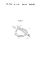
- FIG. 1 A silicon wafer 1 is mounted on a carbon plate heater 2.
- a carbon strip heater 3 moves over the silicon wafer 1.
- the carbon plate heater 2 heats the bulk of the silicon wafer 1 overall by conduction, while the carbon strip heater 3 anneals by heat radiation a local region of the silicon wafer 1.
- the beam of heat from the carbon strip heater 3 melts the local region so as to transform the polycrystalline silicon to monocrystalline silicon.
- FIG. 2 is a schematic view of an embodiment according to the present invention.
- a silicon wafer 1 is covered with an oxide layer 4 and a polycrystalline silicon layer 5.
- the wafer 1 moves toward the direction A relative to lamps 6a, 6b located at opposite sides thereof.
- the first lamp 6a is located at the front of an oxide cap layer 7 and is provided with an elliptical semicylindrical reflective mirror 8a for focusing the beam of heat at a region 5ab to be melted.
- the second lamp 6b provided with an elliptical semicylindrical reflective mirror 8b, is located at the back of the bulk of the silicon wafer 1.
- the lamps are preferably rod-like lamps, such as halogen or inert-gas filled tungsten lamps or mercury discharge lamps.
- the beams of heat emitted from the two lamps are focused on the same region 5ab.
- the second lamp 6b may have less power than the first lamp 6a.
- a similar silicon wafer 1 is irradiated with beams of heat emitted from two lamps 9a, 9b, both located at the front of the silicon wafer 1.
- a single elliptical semicylindrical reflective mirror 10 is provided for the two lamps 9a, 9b, thus reducing the size and simplifying the structure of the heat sources.
- the lamp 9a heats a narrow region 5a
- the lamp 9b heats a broader region 5b. This also reduces the thermal strain.
- the sample comprised a crystal surface (100) p-type silicon wafer 1 of 400 um thickness having an As ion-implanted layer 1a and sequentially thereon a Si 3 N 4 layer 4a, a phosphosilicate glass (PSG) insulator layer 4b, another Si 3 N 4 layer 4c, a polycrystalline silicon layer 5 of 0.4 um thickness, and a thick PSG cap layer 7.
- a crystal surface (100) p-type silicon wafer 1 of 400 um thickness having an As ion-implanted layer 1a and sequentially thereon a Si 3 N 4 layer 4a, a phosphosilicate glass (PSG) insulator layer 4b, another Si 3 N 4 layer 4c, a polycrystalline silicon layer 5 of 0.4 um thickness, and a thick PSG cap layer 7.
- PSG phosphosilicate glass
- the sample was inserted between two halogen-filled tungsten lamps as shown in FIG. 2.
- the two lamps 6a, 6b irradiated the sample with beams of heat focused at region 5ab.
- the front and back beams had a thermal density of 500 W/cm 2 and 100 W/cm 2 , respectively.
- the relative speed of movement of the sample to the beams was 5.4 cm/min.
- the polycrystalline silicon layer 5 was melted and transformed to a monocrystalline layer 5c.
- FIG. 6 shows the impurity profile of semiconductor wafers, i.e., the relationship between the depth of the semiconductor wafer and the concentration of the impurity.
- Curve 1 shows the profile of As ion impurity as implanted with a dose rate of 2 ⁇ 10 15 /cm 2 at 150 keV.
- Curve 2 shows the profile immediately after growing the layers 4a, 4b, 4c, 5, and 7, shown in FIG. 4.
- Curve 3 shows the profile after annealing of the layer 5 so as to form a monocrystalline silicon layer according to the present invention.
- Curve 4 is comparative and shows the profile after annealing the wafer as a whole at 1,050° C. for 10 minutes. With respect to such results in a conventional furnace, it can be seen that the redistribution of the implanted impurity is negligibly small after recrystallizing the polycrystalline silicon layer according to the present invention.
- the thickness of the polycrystalline silicon layer 5 was 0.5 um.
- the heat sources were argon-filled tungsten lamps 9a, 9b, provided with a single elliptical semicylindrical reflective mirror 10.
- One lamp 9a was located at the focal line of the elliptical of the mirror 10, while the other lamp 9b was located just above the same focal line.
- the beam of heat from the lamp 9a focused on a region 5a of the polycrystalline silicon layer 5.
- the beam of heat from the lamp 9b was not focused on the region 5a, but was diffused over a wider region 5b.
- the scanning speed of the sample was 6.0 cm/min.
- the polycrystalline silicon layer 5 was melted and transformed to superior quality monocrystalline silicon region 5c.
- the diffusion of the beam of heat from the lamp 9b had the effect of reducing the thermal strain in the monocrystalline silicon layer 5c.
- Example 1 We subjected a semiconductor wafer 1 similar to that of Example 1 to an irradiating test with two rod-like carbon heaters 11a, 11b located at oppposite sides of the wafer, as shown in FIG. 5.
- the front heater 11a was located 1 mm above the wafer 1
- the back heater 11b was located 5 mm under the wafer 1.
- the heaters were heated to a surface temperature of about 1,500° C. They scanned the wafer at a speed of 6.0 cm/min toward the direction A and melted a polycrystalline silicon layer in line 5ab to transform it into monocrystalline silicon.
- the test was conducted in a nitrogen atmosphere. A similar result was obtained as that in Example 1 with respect to the recrystallization of the polycrystalline silicon layer and the redistribution of the impurity.
Abstract
A process for producing a monocrystalline layer on an insulator, particularly in a semiconductor wafer adapted for use to produce large-scale integrated circuits, comprising the steps of providing a nonmonocrystalline layer on an insulator and heating a region of the nonmonocrystalline layer by irradiating it from two heat sources while moving the heat sources relative to the nomonocrystalline layer, thereby locally melting and transforming the nonmonocrystalline layer to a monocrystalline layer.
Description
The present invention relates to a process for producing a monocrystalline layer on an insulator and, more particularly, for growing a monocrystalline layer by locally annealing for a short time a nonmonocrystalline layer formed on an insulator on a semiconductor wafer.
Considerable research has been performed with the goal of producing a monocrystalline layer of silicon on an insulator, and particularly for producing three-dimensional large-scale integrated circuits (LSI's). A silicon wafer for such use generally accommodates three-dimensional LSI's in the bulk of the wafer.
In the prior art, the silicon wafer is mounted on a carbon plate heater to heat the entire bulk of the wafer by conduction to about 1,200° C. At the same time, a carbon strip heater moves over the silicon wafer to anneal by heat radiation a local region of the wafer at about 1,420° C., the melting point of silicon. The beam of heat from the carbon strip heater melts the local region so as to transform the polycrystalline silicon to monocrystalline silicon. Semiconductor elements can then be formed on the silicon monocrystalline layer. The overall heating and local annealing of the wafer, of course, are conducted in an inert atmosphere so as to reduce oxidation and evaporation of the carbon.
This prior art, however, has the drawback that the protracted heating of the overall wafer at 1,200° C. causes rediffusion of the impurity previously implanted in the wafer. This in turn leads to deteriorated performance of the produced LSI's.
S. Iwamatsu discloses, in Japanese Unexamined Patent Publication (Kokai) No. 56-80138, using a rod-like heat source, such as a xenon lamp provided with a reflective mirror, to scan an energy beam having a linear section over a semiconductor wafer or a layer deposited thereon. From our experience, however, it is substantially impossible for a single commercially available lamp to melt a portion of a semiconductor wafer and transform a nonmonocrystalline layer of silicon to a monocrystalline layer due to its low emitting power, even if the beam is focused thereon.
M. Haond et al disclose, in Electronics Letters, Aug. 19, 1982, vol. 18, No. 17, using a plurality of low-power halogen lamps to preheat a wafer from the back side to a temperature of 300° C. to 1100° C. and using a beam focused on the front surface to supply the additional amount of energy necessary to reach a temperature from 1,000° C. to the melting point of silicon on a certain spot, typically 1 cm in diameter. This annealing is carried out in ambient air while the sample is moved along a spiral at a constant speed. We consider, however, that in this setup, the wafer is still heated as a whole from the back side by the plurality of lamps, which leads to rediffusion of a previously implanted impurity.
It is a primary object of the present invention to provide a process for producing a monocrystalline layer on an insulator.
It is another object of the present invention to provide a process for producing a monocrystalline layer on an insulator with reduced thermal strain in the monocrystalline layer.
It is still another object of the present invention to provide a process for producing a monocrystalline layer on an insulator provided in a semiconductor wafer with reduced rediffusion of the previously implanted impurity.
According to the present invention, there is provided a process for producing a monocrystalline layer on an insulator, particularly in a wafer adapted for use in producing LSI's, comprising the steps of providing a nonmonocrystalline layer on an insulator and heating a region of the monocrystalline layer by irradiation from two heat sources while moving the heat sources relative to the nonmonocrystalline layer, thereby locally melting and transforming the nonmonocrystalline layer to a monocrystalline layer.
These and other objects and advantages of the present invention will become apparent from the ensuing description of the preferred embodiments made with reference to the accompanying figures, wherein:
FIG. 1 is a schematic view of a process for annealing a nonmonocrystalline layer according to a prior art;
FIG. 2 is a schematic view of an embodiment according to the present invention;
FIG. 3 is a schematic view of another embodiment according to the present invention;
FIG. 4 is a sectional view of a semiconductor wafer in which a nonmonocrystalline layer is formed on an insulator;
FIG. 5 is a schematic view of still another embodiment according to the present invention; and
FIG. 6 is a graph of the relationship between the concentration of the impurity and the depth in a semiconductor wafer.
The prior art will be schematically illustrated referring to FIG. 1. A silicon wafer 1 is mounted on a carbon plate heater 2. A carbon strip heater 3 moves over the silicon wafer 1. The carbon plate heater 2 heats the bulk of the silicon wafer 1 overall by conduction, while the carbon strip heater 3 anneals by heat radiation a local region of the silicon wafer 1. Although not shown in the figure, the beam of heat from the carbon strip heater 3 melts the local region so as to transform the polycrystalline silicon to monocrystalline silicon.
FIG. 2 is a schematic view of an embodiment according to the present invention. Referring to FIG. 2, a silicon wafer 1 is covered with an oxide layer 4 and a polycrystalline silicon layer 5. The wafer 1 moves toward the direction A relative to lamps 6a, 6b located at opposite sides thereof. The first lamp 6a is located at the front of an oxide cap layer 7 and is provided with an elliptical semicylindrical reflective mirror 8a for focusing the beam of heat at a region 5ab to be melted. The second lamp 6b, provided with an elliptical semicylindrical reflective mirror 8b, is located at the back of the bulk of the silicon wafer 1.
The lamps are preferably rod-like lamps, such as halogen or inert-gas filled tungsten lamps or mercury discharge lamps.
In FIG. 2, the beams of heat emitted from the two lamps are focused on the same region 5ab. To reduce the thermal strain at the transformed monocrystalline layer 5c, however, it is possible to widen the focus of one of the beams at the region 5ab. Also, the second lamp 6b may have less power than the first lamp 6a.
Referring to FIG. 3, a similar silicon wafer 1 is irradiated with beams of heat emitted from two lamps 9a, 9b, both located at the front of the silicon wafer 1. A single elliptical semicylindrical reflective mirror 10 is provided for the two lamps 9a, 9b, thus reducing the size and simplifying the structure of the heat sources. During relative movement of the silicon wafer 1 in the direction A, the lamp 9a heats a narrow region 5a, while the lamp 9b heats a broader region 5b. This also reduces the thermal strain.
In order to test the effect of the present invention, we used a semiconductor wafer sample as shown in FIG. 4. The sample comprised a crystal surface (100) p-type silicon wafer 1 of 400 um thickness having an As ion-implanted layer 1a and sequentially thereon a Si3 N4 layer 4a, a phosphosilicate glass (PSG) insulator layer 4b, another Si3 N4 layer 4c, a polycrystalline silicon layer 5 of 0.4 um thickness, and a thick PSG cap layer 7.
The sample was inserted between two halogen-filled tungsten lamps as shown in FIG. 2. The two lamps 6a, 6b irradiated the sample with beams of heat focused at region 5ab. The front and back beams had a thermal density of 500 W/cm2 and 100 W/cm2, respectively. The relative speed of movement of the sample to the beams was 5.4 cm/min. Thus, the polycrystalline silicon layer 5 was melted and transformed to a monocrystalline layer 5c.
FIG. 6 shows the impurity profile of semiconductor wafers, i.e., the relationship between the depth of the semiconductor wafer and the concentration of the impurity. Curve 1 shows the profile of As ion impurity as implanted with a dose rate of 2×10¹⁵ /cm2 at 150 keV. Curve 2 shows the profile immediately after growing the layers 4a, 4b, 4c, 5, and 7, shown in FIG. 4. Curve 3 shows the profile after annealing of the layer 5 so as to form a monocrystalline silicon layer according to the present invention. Curve 4 is comparative and shows the profile after annealing the wafer as a whole at 1,050° C. for 10 minutes. With respect to such results in a conventional furnace, it can be seen that the redistribution of the implanted impurity is negligibly small after recrystallizing the polycrystalline silicon layer according to the present invention.
We conducted a similar annealing test using the arrangement shown in FIG. 3. The thickness of the polycrystalline silicon layer 5 was 0.5 um. The heat sources were argon-filled tungsten lamps 9a, 9b, provided with a single elliptical semicylindrical reflective mirror 10. One lamp 9a was located at the focal line of the elliptical of the mirror 10, while the other lamp 9b was located just above the same focal line. The beam of heat from the lamp 9a focused on a region 5a of the polycrystalline silicon layer 5. The beam of heat from the lamp 9b was not focused on the region 5a, but was diffused over a wider region 5b. The scanning speed of the sample was 6.0 cm/min. The polycrystalline silicon layer 5 was melted and transformed to superior quality monocrystalline silicon region 5c. The diffusion of the beam of heat from the lamp 9b had the effect of reducing the thermal strain in the monocrystalline silicon layer 5c.
We subjected a semiconductor wafer 1 similar to that of Example 1 to an irradiating test with two rod- like carbon heaters 11a, 11b located at oppposite sides of the wafer, as shown in FIG. 5. The front heater 11a was located 1 mm above the wafer 1, and the back heater 11b was located 5 mm under the wafer 1. The heaters were heated to a surface temperature of about 1,500° C. They scanned the wafer at a speed of 6.0 cm/min toward the direction A and melted a polycrystalline silicon layer in line 5ab to transform it into monocrystalline silicon. The test was conducted in a nitrogen atmosphere. A similar result was obtained as that in Example 1 with respect to the recrystallization of the polycrystalline silicon layer and the redistribution of the impurity.
Claims (8)
1. A process for producing a monocrystalline layer on an insulating layer formed on a front side of a semiconductor substrate having at least one impurity region containing impurities under said insulating layer, comprising the steps of:
providing a nonmonocrystalline layer with a back side on said insulating layer over said at least one impurity region in said substrate; and
heating a local portion of said nonmonocrystalline layer without causing substantial redistribution of said impurities in said at least one impurity region by irradiating said local portion with two energy beams emitted from two respective rod-like heat sources located apart from and parallel to said substrate, wherein a first of said energy beams irradiates said nonmonocrystalline layer from the front side of said nonmonocrystalline layer with an energy density that is larger than that of the other energy beam, and said other energy beam irradiates either the front side of said nonmonocrystalline layer or a back side of said substrate, while moving said energy beams relative to said nonmonocrystalline layer, wherein said nonmonocrystaline layer is locally melted and transformed to a monocrystalline layer during said moving as a result of the irradiation.
2. A process according to claim 1, wherein said two heat sources are located at opposite sides of said nonmonocrystalline layer.
3. A process according to claim 2, wherein said heat sources are rod-like lamps, each provided with a respective elliptical semicylindrical reflecting mirror, at least one of said lamps is located at said front side of said nonmonocrystalline layer along a focal line of an ellipse of the respective elliptical semicylindrical reflective mirror, and provides an irradiated region which is located at the other focal line of said ellipse.
4. A process according to claim 3, said rod-like lamps being selected from the group consisting of halogen and inert-gas filled tungsten lamps and mercury discharge lamps.
5. A process according to claim 2, wherein said heat sources are rod-like carbon heaters.
6. A process according to claim 1, wherein said two heat sources are located at the same side of said nonmonocrystalline layer.
7. A process according to claim 6, wherein said heat sources are rod-like lamps, each provided with an elliptical semicylindrical reflective mirror, at least one of said lamps is located at said front side of said nonmonocrystalline layer along a focal line of an ellipse of the respective elliptical semicylindrical reflective mirror, and provides an irradiated region which is located at the other focal line of said ellipse.
8. A process according to claim 7, said rod-like lamps being selected from the group consisting of halogen and inert-gas filled tungsten lamps and mercury discharge lamps.
Applications Claiming Priority (2)
| Application Number | Priority Date | Filing Date | Title |
|---|---|---|---|
| JP58-055873 | 1983-03-31 | ||
| JP58055873A JPS59205711A (en) | 1983-03-31 | 1983-03-31 | Manufacture of semiconductor device |
Publications (1)
| Publication Number | Publication Date |
|---|---|
| US4659422A true US4659422A (en) | 1987-04-21 |
Family
ID=13011206
Family Applications (1)
| Application Number | Title | Priority Date | Filing Date |
|---|---|---|---|
| US06/592,067 Expired - Fee Related US4659422A (en) | 1983-03-31 | 1984-03-22 | Process for producing monocrystalline layer on insulator |
Country Status (4)
| Country | Link |
|---|---|
| US (1) | US4659422A (en) |
| EP (1) | EP0124261B1 (en) |
| JP (1) | JPS59205711A (en) |
| DE (1) | DE3465829D1 (en) |
Cited By (17)
| Publication number | Priority date | Publication date | Assignee | Title |
|---|---|---|---|---|
| US4707217A (en) * | 1986-05-28 | 1987-11-17 | The United States Of America As Represented By The Secretary Of The Navy | Single crystal thin films |
| US4743567A (en) * | 1987-08-11 | 1988-05-10 | North American Philips Corp. | Method of forming thin, defect-free, monocrystalline layers of semiconductor materials on insulators |
| US4888302A (en) * | 1987-11-25 | 1989-12-19 | North American Philips Corporation | Method of reduced stress recrystallization |
| US4950614A (en) * | 1984-05-15 | 1990-08-21 | Semiconductor Energy Laboratory Co., Ltd. | Method of making a tandem type semiconductor photoelectric conversion device |
| US4971919A (en) * | 1984-05-15 | 1990-11-20 | Semiconductor Energy Laboratory Co., Ltd. | Semiconductor photoelectric conversion device and method of making the same |
| US5066610A (en) * | 1987-11-20 | 1991-11-19 | Massachusetts Institute Of Technology | Capping technique for zone-melting recrystallization of insulated semiconductor films |
| US5160575A (en) * | 1985-12-04 | 1992-11-03 | Massachusetts Institute Of Technology | Edge-heat sink technqiue for zone melting recrystallization of semiconductor-on-insulator films |
| US5173271A (en) * | 1985-12-04 | 1992-12-22 | Massachusetts Institute Of Technology | Enhanced radiative zone-melting recrystallization method and apparatus |
| US5296089A (en) * | 1985-12-04 | 1994-03-22 | Massachusetts Institute Of Technology | Enhanced radiative zone-melting recrystallization method and apparatus |
| US20020127830A1 (en) * | 1997-03-11 | 2002-09-12 | Semiconductor Energy Laboratory Co., Ltd., A Japan Corporation | Heating treatment device, heating treatment method and fabrication method of semiconductor device |
| US20030203656A1 (en) * | 1999-08-18 | 2003-10-30 | Semiconductor Energy Laboratory Co., Ltd. | Semiconductor device, manufacturing method thereof, and electronic device |
| US20040087156A1 (en) * | 2002-10-17 | 2004-05-06 | Semiconductor Energy Laboratory Co., Ltd. | Method of manufacturing semiconductor device |
| US20040203219A1 (en) * | 1999-08-18 | 2004-10-14 | Semiconductor Energy Laboratory Co., Ltd. | Laser apparatus and laser annealing method |
| US20050042847A1 (en) * | 1997-02-10 | 2005-02-24 | Semiconductor Energy Laboratory Co., Ltd., A Japan Corporation | Manufacturing method of semiconductor and manufacturing method of semiconductor device |
| US6927109B1 (en) * | 1999-07-05 | 2005-08-09 | Semiconductor Energy Laboratory Co., Ltd. | Laser irradiation apparatus laser irradiation method, semiconductor device and method of manufacturing a semiconductor device |
| DE102004044709A1 (en) * | 2004-09-15 | 2006-03-16 | Fraunhofer-Gesellschaft zur Förderung der angewandten Forschung e.V. | Process for the simultaneous recrystallization and doping of semiconductor layers and semiconductor layer systems produced by this process |
| US7078321B2 (en) * | 2000-06-19 | 2006-07-18 | Semiconductor Energy Laboratory Co., Ltd. | Semiconductor device and method of manufacturing the same |
Families Citing this family (4)
| Publication number | Priority date | Publication date | Assignee | Title |
|---|---|---|---|---|
| KR890008943A (en) * | 1987-11-25 | 1989-07-13 | 이반 밀러 레르너 | Method of manufacturing single crystal layer on substrate |
| JPH04364031A (en) * | 1991-06-10 | 1992-12-16 | Ii & S:Kk | Method and apparatus for laser annealing |
| US5338388A (en) * | 1992-05-04 | 1994-08-16 | Mitsubishi Denki Kabushiki Kaisha | Method of forming single-crystal semiconductor films |
| JP2006032982A (en) * | 2005-09-02 | 2006-02-02 | Semiconductor Energy Lab Co Ltd | Heating processing method of thin film |
Citations (14)
| Publication number | Priority date | Publication date | Assignee | Title |
|---|---|---|---|---|
| US3096158A (en) * | 1959-09-25 | 1963-07-02 | Gerthart K Gaule | Apparatus for pulling single crystals in the form of long flat strips from a melt |
| US3585088A (en) * | 1968-10-18 | 1971-06-15 | Ibm | Methods of producing single crystals on supporting substrates |
| US3695941A (en) * | 1966-09-20 | 1972-10-03 | Geoffrey William Green | Preparation of eutectic material |
| US4081313A (en) * | 1975-01-24 | 1978-03-28 | Applied Materials, Inc. | Process for preparing semiconductor wafers with substantially no crystallographic slip |
| US4120743A (en) * | 1975-12-31 | 1978-10-17 | Motorola, Inc. | Crossed grain growth |
| US4309225A (en) * | 1979-09-13 | 1982-01-05 | Massachusetts Institute Of Technology | Method of crystallizing amorphous material with a moving energy beam |
| US4371421A (en) * | 1981-04-16 | 1983-02-01 | Massachusetts Institute Of Technology | Lateral epitaxial growth by seeded solidification |
| US4410562A (en) * | 1980-11-29 | 1983-10-18 | Dainippon Ink And Chemicals, Inc. | Method for forming a cured resin coating having a desired pattern on the surface of a substrate |
| GB2119680A (en) * | 1982-05-03 | 1983-11-23 | Gca Corp | Apparatus for heat treating a semiconductor wafer |
| JPS598691A (en) * | 1982-07-06 | 1984-01-17 | Alps Electric Co Ltd | Microzone melting process |
| US4427723A (en) * | 1982-02-10 | 1984-01-24 | Rockwell International Corporation | Method and apparatus for laser-stimulated vacuum deposition and annealing technique |
| US4476154A (en) * | 1981-06-29 | 1984-10-09 | Tokyo Shibaura Denki Kabushiki Kaisha | Method of manufacturing a glass passivation semiconductor device |
| JPS59181189A (en) * | 1983-03-31 | 1984-10-15 | ジューキ株式会社 | Needle yarn feeder of sewing machine |
| US4479846A (en) * | 1982-06-23 | 1984-10-30 | Massachusetts Institute Of Technology | Method of entraining dislocations and other crystalline defects in heated film contacting patterned region |
Family Cites Families (2)
| Publication number | Priority date | Publication date | Assignee | Title |
|---|---|---|---|---|
| JPS5797620A (en) * | 1980-12-11 | 1982-06-17 | Fujitsu Ltd | Improvement of crystallinity of semiconductor film |
| JPS5943811B2 (en) * | 1981-09-16 | 1984-10-24 | ウシオ電機株式会社 | Method for epitaxial growth of amorphous silicon or polycrystalline silicon on a wafer |
-
1983
- 1983-03-31 JP JP58055873A patent/JPS59205711A/en active Pending
-
1984
- 1984-03-22 US US06/592,067 patent/US4659422A/en not_active Expired - Fee Related
- 1984-03-28 DE DE8484302118T patent/DE3465829D1/en not_active Expired
- 1984-03-28 EP EP84302118A patent/EP0124261B1/en not_active Expired
Patent Citations (14)
| Publication number | Priority date | Publication date | Assignee | Title |
|---|---|---|---|---|
| US3096158A (en) * | 1959-09-25 | 1963-07-02 | Gerthart K Gaule | Apparatus for pulling single crystals in the form of long flat strips from a melt |
| US3695941A (en) * | 1966-09-20 | 1972-10-03 | Geoffrey William Green | Preparation of eutectic material |
| US3585088A (en) * | 1968-10-18 | 1971-06-15 | Ibm | Methods of producing single crystals on supporting substrates |
| US4081313A (en) * | 1975-01-24 | 1978-03-28 | Applied Materials, Inc. | Process for preparing semiconductor wafers with substantially no crystallographic slip |
| US4120743A (en) * | 1975-12-31 | 1978-10-17 | Motorola, Inc. | Crossed grain growth |
| US4309225A (en) * | 1979-09-13 | 1982-01-05 | Massachusetts Institute Of Technology | Method of crystallizing amorphous material with a moving energy beam |
| US4410562A (en) * | 1980-11-29 | 1983-10-18 | Dainippon Ink And Chemicals, Inc. | Method for forming a cured resin coating having a desired pattern on the surface of a substrate |
| US4371421A (en) * | 1981-04-16 | 1983-02-01 | Massachusetts Institute Of Technology | Lateral epitaxial growth by seeded solidification |
| US4476154A (en) * | 1981-06-29 | 1984-10-09 | Tokyo Shibaura Denki Kabushiki Kaisha | Method of manufacturing a glass passivation semiconductor device |
| US4427723A (en) * | 1982-02-10 | 1984-01-24 | Rockwell International Corporation | Method and apparatus for laser-stimulated vacuum deposition and annealing technique |
| GB2119680A (en) * | 1982-05-03 | 1983-11-23 | Gca Corp | Apparatus for heat treating a semiconductor wafer |
| US4479846A (en) * | 1982-06-23 | 1984-10-30 | Massachusetts Institute Of Technology | Method of entraining dislocations and other crystalline defects in heated film contacting patterned region |
| JPS598691A (en) * | 1982-07-06 | 1984-01-17 | Alps Electric Co Ltd | Microzone melting process |
| JPS59181189A (en) * | 1983-03-31 | 1984-10-15 | ジューキ株式会社 | Needle yarn feeder of sewing machine |
Non-Patent Citations (2)
| Title |
|---|
| Hess et al., "Laser Annealing", Industrial Research Development, Nov. 1979, pp. 141-152. |
| Hess et al., Laser Annealing , Industrial Research Development, Nov. 1979, pp. 141 152. * |
Cited By (31)
| Publication number | Priority date | Publication date | Assignee | Title |
|---|---|---|---|---|
| US4950614A (en) * | 1984-05-15 | 1990-08-21 | Semiconductor Energy Laboratory Co., Ltd. | Method of making a tandem type semiconductor photoelectric conversion device |
| US4971919A (en) * | 1984-05-15 | 1990-11-20 | Semiconductor Energy Laboratory Co., Ltd. | Semiconductor photoelectric conversion device and method of making the same |
| US5160575A (en) * | 1985-12-04 | 1992-11-03 | Massachusetts Institute Of Technology | Edge-heat sink technqiue for zone melting recrystallization of semiconductor-on-insulator films |
| US5173271A (en) * | 1985-12-04 | 1992-12-22 | Massachusetts Institute Of Technology | Enhanced radiative zone-melting recrystallization method and apparatus |
| US5296089A (en) * | 1985-12-04 | 1994-03-22 | Massachusetts Institute Of Technology | Enhanced radiative zone-melting recrystallization method and apparatus |
| US4707217A (en) * | 1986-05-28 | 1987-11-17 | The United States Of America As Represented By The Secretary Of The Navy | Single crystal thin films |
| US4743567A (en) * | 1987-08-11 | 1988-05-10 | North American Philips Corp. | Method of forming thin, defect-free, monocrystalline layers of semiconductor materials on insulators |
| US5066610A (en) * | 1987-11-20 | 1991-11-19 | Massachusetts Institute Of Technology | Capping technique for zone-melting recrystallization of insulated semiconductor films |
| US4888302A (en) * | 1987-11-25 | 1989-12-19 | North American Philips Corporation | Method of reduced stress recrystallization |
| US7300826B2 (en) | 1997-02-10 | 2007-11-27 | Semiconductor Energy Laboratory Co., Ltd. | Manufacturing method of semiconductor and manufacturing method of semiconductor device |
| US20050042847A1 (en) * | 1997-02-10 | 2005-02-24 | Semiconductor Energy Laboratory Co., Ltd., A Japan Corporation | Manufacturing method of semiconductor and manufacturing method of semiconductor device |
| US20060134929A1 (en) * | 1997-03-11 | 2006-06-22 | Semiconductor Energy Laboratory Co., Ltd. A Japan Corporation | Heating treatment device, heating treatment method and fabrication method of semiconductor device |
| US20020127830A1 (en) * | 1997-03-11 | 2002-09-12 | Semiconductor Energy Laboratory Co., Ltd., A Japan Corporation | Heating treatment device, heating treatment method and fabrication method of semiconductor device |
| US7410850B2 (en) | 1997-03-11 | 2008-08-12 | Semiconductor Energy Laboratory Co., Ltd. | Heating treatment device, heating treatment method and fabrication method of semiconductor device |
| US7214574B2 (en) | 1997-03-11 | 2007-05-08 | Semiconductor Energy Laboratory Co., Ltd. | Heating treatment device, heating treatment method and fabrication method of semiconductor device |
| US6927109B1 (en) * | 1999-07-05 | 2005-08-09 | Semiconductor Energy Laboratory Co., Ltd. | Laser irradiation apparatus laser irradiation method, semiconductor device and method of manufacturing a semiconductor device |
| US7419861B2 (en) | 1999-07-05 | 2008-09-02 | Semiconductor Energy Laboratory Co., Ltd. | Laser irradiation apparatus, laser irradiation method, semiconductor device, and method of manufacturing a semiconductor device |
| US20050247685A1 (en) * | 1999-07-05 | 2005-11-10 | Semiconductor Energy Laboratory Co., Ltd. | Laser irradiation apparatus, laser irradiation method, semiconductor device, and method of manufacturing a semiconductor device |
| US20040203219A1 (en) * | 1999-08-18 | 2004-10-14 | Semiconductor Energy Laboratory Co., Ltd. | Laser apparatus and laser annealing method |
| US7338913B2 (en) | 1999-08-18 | 2008-03-04 | Semiconductor Energy Laboratory Co., Ltd. | Semiconductor device, manufacturing method thereof, and electronic device |
| US20030203656A1 (en) * | 1999-08-18 | 2003-10-30 | Semiconductor Energy Laboratory Co., Ltd. | Semiconductor device, manufacturing method thereof, and electronic device |
| US7456371B2 (en) | 1999-08-18 | 2008-11-25 | Semiconductor Energy Laboratory Co., Ltd. | Laser apparatus and laser annealing method |
| US7307283B2 (en) | 2000-06-19 | 2007-12-11 | Semiconductor Energy Laboratory Co., Ltd. | Semiconductor device and method of manufacturing the same |
| US7078321B2 (en) * | 2000-06-19 | 2006-07-18 | Semiconductor Energy Laboratory Co., Ltd. | Semiconductor device and method of manufacturing the same |
| US20040087156A1 (en) * | 2002-10-17 | 2004-05-06 | Semiconductor Energy Laboratory Co., Ltd. | Method of manufacturing semiconductor device |
| US7332431B2 (en) | 2002-10-17 | 2008-02-19 | Semiconductor Energy Laboratory Co., Ltd. | Method of manufacturing semiconductor device |
| DE102004044709A1 (en) * | 2004-09-15 | 2006-03-16 | Fraunhofer-Gesellschaft zur Förderung der angewandten Forschung e.V. | Process for the simultaneous recrystallization and doping of semiconductor layers and semiconductor layer systems produced by this process |
| US20080311697A1 (en) * | 2004-09-15 | 2008-12-18 | Fraunhofer-Gesellschaft Zur Förderung Der Angewand | Method For Simultaneous Recrystallization and Doping of Semiconductor Layers and Semiconductor Layer Systems Produced According to This Method |
| US7838437B2 (en) | 2004-09-15 | 2010-11-23 | Fraunhofer-Gesellschaft Zur Forderung Der Angewandten Forschung E.V. | Method for simultaneous recrystallization and doping of semiconductor layers |
| US20110018102A1 (en) * | 2004-09-15 | 2011-01-27 | Fraunhofer-Gesellschaft Zur Forderung Der Angewandten Forschung E.V. | Method for Simultaneous Recrystallization and Doping of Semiconductor Layers and Semiconductor Layer Systems Produced According to this Method |
| US8168972B2 (en) | 2004-09-15 | 2012-05-01 | Fraunhofer-Gesellschaft zur Förderung der angewandten Forschung e.V. | Method for simultaneous recrystallization and doping of semiconductor layers and semiconductor layer systems produced according to this method |
Also Published As
| Publication number | Publication date |
|---|---|
| JPS59205711A (en) | 1984-11-21 |
| EP0124261B1 (en) | 1987-09-02 |
| DE3465829D1 (en) | 1987-10-08 |
| EP0124261A1 (en) | 1984-11-07 |
Similar Documents
| Publication | Publication Date | Title |
|---|---|---|
| US4659422A (en) | Process for producing monocrystalline layer on insulator | |
| US4581520A (en) | Heat treatment machine for semiconductors | |
| US4482393A (en) | Method of activating implanted ions by incoherent light beam | |
| US7943534B2 (en) | Semiconductor device manufacturing method and semiconductor device manufacturing system | |
| US4504323A (en) | Method for annealing semiconductors with a planar source composed of flash discharge lamps | |
| US5219786A (en) | Semiconductor layer annealing method using excimer laser | |
| US4439245A (en) | Electromagnetic radiation annealing of semiconductor material | |
| US5017508A (en) | Method of annealing fully-fabricated, radiation damaged semiconductor devices | |
| US4474831A (en) | Method for reflow of phosphosilicate glass | |
| US20110223773A1 (en) | Low temperature process for depositing a high extinction coefficient non-peeling optical absorber for a scanning laser surface anneal of implanted dopants | |
| US4443493A (en) | Laser induced flow glass materials | |
| US5840118A (en) | Laser process system and method of using the same | |
| US20130008878A1 (en) | Thermal flux annealing influence of buried species | |
| US4555273A (en) | Furnace transient anneal process | |
| JP2002246328A (en) | Heat treatment method, heat treatment device and manufacturing method for semiconductor device | |
| US4431900A (en) | Laser induced flow Ge-O based materials | |
| JP2000349042A (en) | Method and apparatus for manufacturing semiconductor device | |
| JPS59211221A (en) | Heat treatment of ion implanted semiconductor | |
| JPS61116820A (en) | Annealing method for semiconductor | |
| JPH0377657B2 (en) | ||
| JPS59178718A (en) | Semiconductor substrate processing apparatus | |
| JPH0420254B2 (en) | ||
| JPH0210569B2 (en) | ||
| JP2001196320A (en) | Doping method, manufacturing method of semiconductor device, manufacturing method of semiconductor element and manufacturing apparatus thereof and doping equipment | |
| JPH05235321A (en) | Method for forming connection structure |
Legal Events
| Date | Code | Title | Description |
|---|---|---|---|
| AS | Assignment |
Owner name: FUJITSU LIMITED 1015 KAMIKODANAKA, NAKAHARA-KU, KA Free format text: ASSIGNMENT OF ASSIGNORS INTEREST.;ASSIGNOR:SAKURAI, JUNJI;REEL/FRAME:004242/0727 Effective date: 19840302 |
|
| CC | Certificate of correction | ||
| FEPP | Fee payment procedure |
Free format text: PAYOR NUMBER ASSIGNED (ORIGINAL EVENT CODE: ASPN); ENTITY STATUS OF PATENT OWNER: LARGE ENTITY |
|
| FPAY | Fee payment |
Year of fee payment: 4 |
|
| REMI | Maintenance fee reminder mailed | ||
| LAPS | Lapse for failure to pay maintenance fees | ||
| FP | Lapsed due to failure to pay maintenance fee |
Effective date: 19950426 |
|
| STCH | Information on status: patent discontinuation |
Free format text: PATENT EXPIRED DUE TO NONPAYMENT OF MAINTENANCE FEES UNDER 37 CFR 1.362 |