US4674939A - Sealed standard interface apparatus - Google Patents
Sealed standard interface apparatus Download PDFInfo
- Publication number
- US4674939A US4674939A US06/635,384 US63538484A US4674939A US 4674939 A US4674939 A US 4674939A US 63538484 A US63538484 A US 63538484A US 4674939 A US4674939 A US 4674939A
- Authority
- US
- United States
- Prior art keywords
- box
- region
- door
- port
- seal
- Prior art date
- Legal status (The legal status is an assumption and is not a legal conclusion. Google has not performed a legal analysis and makes no representation as to the accuracy of the status listed.)
- Expired - Lifetime
Links
Images


Classifications
-
- H—ELECTRICITY
- H01—ELECTRIC ELEMENTS
- H01L—SEMICONDUCTOR DEVICES NOT COVERED BY CLASS H10
- H01L21/00—Processes or apparatus adapted for the manufacture or treatment of semiconductor or solid state devices or of parts thereof
- H01L21/67—Apparatus specially adapted for handling semiconductor or electric solid state devices during manufacture or treatment thereof; Apparatus specially adapted for handling wafers during manufacture or treatment of semiconductor or electric solid state devices or components ; Apparatus not specifically provided for elsewhere
- H01L21/68—Apparatus specially adapted for handling semiconductor or electric solid state devices during manufacture or treatment thereof; Apparatus specially adapted for handling wafers during manufacture or treatment of semiconductor or electric solid state devices or components ; Apparatus not specifically provided for elsewhere for positioning, orientation or alignment
-
- H—ELECTRICITY
- H01—ELECTRIC ELEMENTS
- H01L—SEMICONDUCTOR DEVICES NOT COVERED BY CLASS H10
- H01L21/00—Processes or apparatus adapted for the manufacture or treatment of semiconductor or solid state devices or of parts thereof
- H01L21/67—Apparatus specially adapted for handling semiconductor or electric solid state devices during manufacture or treatment thereof; Apparatus specially adapted for handling wafers during manufacture or treatment of semiconductor or electric solid state devices or components ; Apparatus not specifically provided for elsewhere
- H01L21/677—Apparatus specially adapted for handling semiconductor or electric solid state devices during manufacture or treatment thereof; Apparatus specially adapted for handling wafers during manufacture or treatment of semiconductor or electric solid state devices or components ; Apparatus not specifically provided for elsewhere for conveying, e.g. between different workstations
- H01L21/67763—Apparatus specially adapted for handling semiconductor or electric solid state devices during manufacture or treatment thereof; Apparatus specially adapted for handling wafers during manufacture or treatment of semiconductor or electric solid state devices or components ; Apparatus not specifically provided for elsewhere for conveying, e.g. between different workstations the wafers being stored in a carrier, involving loading and unloading
- H01L21/67772—Apparatus specially adapted for handling semiconductor or electric solid state devices during manufacture or treatment thereof; Apparatus specially adapted for handling wafers during manufacture or treatment of semiconductor or electric solid state devices or components ; Apparatus not specifically provided for elsewhere for conveying, e.g. between different workstations the wafers being stored in a carrier, involving loading and unloading involving removal of lid, door, cover
-
- H—ELECTRICITY
- H01—ELECTRIC ELEMENTS
- H01L—SEMICONDUCTOR DEVICES NOT COVERED BY CLASS H10
- H01L21/00—Processes or apparatus adapted for the manufacture or treatment of semiconductor or solid state devices or of parts thereof
- H01L21/67—Apparatus specially adapted for handling semiconductor or electric solid state devices during manufacture or treatment thereof; Apparatus specially adapted for handling wafers during manufacture or treatment of semiconductor or electric solid state devices or components ; Apparatus not specifically provided for elsewhere
- H01L21/677—Apparatus specially adapted for handling semiconductor or electric solid state devices during manufacture or treatment thereof; Apparatus specially adapted for handling wafers during manufacture or treatment of semiconductor or electric solid state devices or components ; Apparatus not specifically provided for elsewhere for conveying, e.g. between different workstations
- H01L21/67763—Apparatus specially adapted for handling semiconductor or electric solid state devices during manufacture or treatment thereof; Apparatus specially adapted for handling wafers during manufacture or treatment of semiconductor or electric solid state devices or components ; Apparatus not specifically provided for elsewhere for conveying, e.g. between different workstations the wafers being stored in a carrier, involving loading and unloading
- H01L21/67775—Docking arrangements
-
- H—ELECTRICITY
- H05—ELECTRIC TECHNIQUES NOT OTHERWISE PROVIDED FOR
- H05K—PRINTED CIRCUITS; CASINGS OR CONSTRUCTIONAL DETAILS OF ELECTRIC APPARATUS; MANUFACTURE OF ASSEMBLAGES OF ELECTRICAL COMPONENTS
- H05K13/00—Apparatus or processes specially adapted for manufacturing or adjusting assemblages of electric components
- H05K13/02—Feeding of components
-
- Y—GENERAL TAGGING OF NEW TECHNOLOGICAL DEVELOPMENTS; GENERAL TAGGING OF CROSS-SECTIONAL TECHNOLOGIES SPANNING OVER SEVERAL SECTIONS OF THE IPC; TECHNICAL SUBJECTS COVERED BY FORMER USPC CROSS-REFERENCE ART COLLECTIONS [XRACs] AND DIGESTS
- Y10—TECHNICAL SUBJECTS COVERED BY FORMER USPC
- Y10S—TECHNICAL SUBJECTS COVERED BY FORMER USPC CROSS-REFERENCE ART COLLECTIONS [XRACs] AND DIGESTS
- Y10S414/00—Material or article handling
- Y10S414/135—Associated with semiconductor wafer handling
- Y10S414/139—Associated with semiconductor wafer handling including wafer charging or discharging means for vacuum chamber
-
- Y—GENERAL TAGGING OF NEW TECHNOLOGICAL DEVELOPMENTS; GENERAL TAGGING OF CROSS-SECTIONAL TECHNOLOGIES SPANNING OVER SEVERAL SECTIONS OF THE IPC; TECHNICAL SUBJECTS COVERED BY FORMER USPC CROSS-REFERENCE ART COLLECTIONS [XRACs] AND DIGESTS
- Y10—TECHNICAL SUBJECTS COVERED BY FORMER USPC
- Y10S—TECHNICAL SUBJECTS COVERED BY FORMER USPC CROSS-REFERENCE ART COLLECTIONS [XRACs] AND DIGESTS
- Y10S414/00—Material or article handling
- Y10S414/135—Associated with semiconductor wafer handling
- Y10S414/14—Wafer cassette transporting
Definitions
- the present invention relates to standardized mechanical interface systems for reducing particle contamination and more particularly to apparatus employing sealed containers suitable for use in semiconductor processing equipment to prevent particle contamination.
- a standardized mechanical interface has been proposed to reduce particle contamination by significantly reducing particle fluxes onto wafers. This end is accomplished by mechanically ensuring that during transport, storage and processing of the wafers, the gaseous media (such as air or nitrogen) surrounding the wafers is essentially stationary relative to the wafers and by ensuring that particles from the ambient outside environment do not enter the immediate internal wafer environment.
- the gaseous media such as air or nitrogen
- contamination particles cause incomplete etching in spaces between lines, thus leading to an unwanted electrical bridge.
- other contamination particles may cause electrical failure due to induced ionization or trapping centers in gate dielectrics or junctions.
- the main sources of particulate contamination are personnel, equipment, and chemicals. Particles given off by personnel are transmitted through the environment and through physical contact or migration onto the wafer surface. People, by shedding of skin flakes, for example, are a significant source of particles that are easily ionized and cause defects. Although clean room garments reduce particle emissions they do not fully contain the emissions. It has been found that as many as 6000 particles per minute are emitted into an adjacent one cubic foot of space by a fully suited operator.
- process defects Particles within the equipment and chemicals are termed "process defects.” To minimize process defects, processing equipment manufacturers must prevent machine generated particles from reaching the wafers, and suppliers of gases and liquid chemicals must deliver cleaner products. Most important, a system must be designed that will effectively isolate wafers from particles during storage, transport and transfer into processing equipment.
- SMIF Standard Mechanical Interface
- the SMIF concept is based on the realization that a small volume of still, particle-free air, with no internal source of particles, is the cleanest possible environment for wafers. Further details of one proposed system are described in the article "SMIF: A TECHNOLOGY FOR WAFER CASSETTE TRANSFER IN VLSI MANUFACTURING", by Mihir Parikh and Ulrich Kaempf, Solid State Technology, July 1984, pp. 111-115.
- the proposed SMIF system has three main components, namely, (1) minimum volume, dustproof boxes are used for storing and transporting wafer cassettes; (2) canopies are placed over cassette ports of processing equipment so that the environments inside the boxes and canopies become miniature clean spaces; (3) doors on the boxes are designed to mate with doors on the interface ports on the equipment canopies and the two doors are opened simultaneously so that particles which may have been on the external door surfaces are trapped (“sandwiched") between the doors.
- a box is placed at the interface port on top of the canopy; latches release the box door and the canopy port door simultaneously.
- a mechanical elevator lowers the two doors, with the cassette riding on top, into the canopy covered space.
- a manipulator picks up the cassette and places it onto the cassette port/elevator of the equipment. After processing, the reverse operation takes place.
- the SMIF system has been proved effective by experiments using prototype SMIF components both inside and outside a clean room.
- the SMIF configuration achieved a ten-fold improvement over the conventional handling of open cassettes inside the clean room.
- the present invention is an apparatus for maintaining articles, such as semiconductor wafers clean.
- the wafers or other articles to be processed are placed in a box having first and second regions for making first and second seals.
- a box door seals the articles into the box.
- the box has a second region for making the second seal and has a third region for making a third seal.
- the box is used to transport the wafers to a port in the canopy of the processing equipment.
- the port is adapted for receiving the box and box door and for transferring the box door and the contents of the box into a region beneath the canopy.
- the canopy has a first region for making the first seal with the box.
- the port has a fourth region surrounding the port opening for making a fourth seal.
- a port door is provided for closing the port when no box is present.
- the port door has a second region for making the second seal with the box and has a fourth region for making the fourth seal with the port.
- a box door latch is provided for latching the box door to the box whereby the second seal is made and released in the second region between the box door and the box by operation of the box door latch.
- a box latch is provided for latching the box to the port whereby the first seal is made or released in the first region between the box and the port by the operation of the box latch.
- first and second regions where first and second seals are made on the box are spaced apart and the box door latch operates between the walls of the box and the box door in the space between the first and second regions.
- the box door latch need only be operated to release the second seal after the first seal has been engaged.
- the box door latch mechanism is operated from inside the latch door in an internal space, through the latch door wall to the box wall and no opening to the outside environment occurs as a result of the box door latch mechanism or its operation.
- the box door latch includes spring loaded latches which are normally closed to latch the box door to the box.
- the springs are engaged and disengaged by spring actuators contained within the port door mechanism whenever the box and box door are placed upon or are removed from the canopy port.
- the various embodiments of the invention the springs and other latch mechanism from the clean regions to regions which, although contaminated, do not affect the clean regions thereby providing improved interface mechanisms.
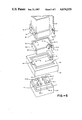
- FIG. 1 depicts a perspective view of the SMIF system positioned adjacent processing equipment.
- FIG. 2 depicts a schematic representation of the SMIF system and the processing equipment of FIG. 1.
- FIG. 3 depicts an exploded perspective view of a port assembly of the present invention.
- FIG. 4 depicts a front view of the SMIF box and a portion of the port assembly.
- FIG. 5 depicts a side view of the FIG. 4 apparatus.
- FIG. 6 depicts a top view of the FIG. 4 apparatus.
- FIG. 7 depicts a front view of the box latch mechanism by which the box is latched to the port plate of the canopy of FIG. 2.
- FIG. 8 depicts a perspective view of the solenoid and connecting mechanism which actuates the box door latch springs.
- FIGS. 9-11 depict various different pins which are employed as alternatives for the pins of FIG. 8.
- FIG. 12 depicts an exploded partial sectional front view of the port assembly with the box and box door positioned above the port with the port door closed.
- FIG. 13 depicts a cross-sectional side view of the FIG. 12 apparatus when the box and box door have been positioned on the port plate so that all seals are closed.
- FIG. 14 depicts the apparatus of FIG. 13 in an exploded view with the box door and the port door connected and withdrawn to open the port.
- FIG. 15 depicts an alternate embodiment of the box door latch mechanism.
- a canopy 10 is an easily removable shield that covers the wafer-handling mechanisms of the processing equipment 15.
- Equipment 15 is a photoresist applicator, mask aligner, inspection station, or any similar processing equipment.
- the canopy 10 is constructed of transparent plastic such as Lexan to facilitate inspection and/or maintenance within the canopy 10.
- the canopy 10 encloses the handling mechanisms of the processing equipment 15 and a wafer cassette 80 holding wafers 82 and therefore the equipment 15 need not be installed in a clean room.
- FIG. 2 shows further details of the FIG. 1 apparatus.
- a box 90 is mounted on an horizontal surface 40 of the canopy 10 by means of a part plate 50.
- a port assembly 20 further includes a port door 60 and an elevator mechanism 70 that transports the cassette 80, containing the integrated circuit wafers 82, from the box 90 into the region beneath the canopy 10.
- the port door 60 and the box door 99 are shown in the closed positions by broken lines and are shown in the open position by solid lines.
- a mover assembly 29 includes a platform 26, a shaft engagement means 72, and a drive motor 28.
- the platform 26 is attached by engagement means 72 to a vertical guide 71 of elevator assembly 70.
- guide 71 includes a lead screw (not shown) and motor 28 drives a gear (not shown) which engages the lead screw for driving the platform 26 up or down.
- the port door 60 closes the port opening in the canopy 10.
- a manipulator assembly 30 is fastened to a platform 27 which has an engagement means 73 for engaging the vertical shaft assembly 71.
- Manipulator 30 includes a manipulator arm 31 and an engagement head 32 adapted to engage the cassette 80.
- FIG. 3 an exploded, perspective view of the port assembly 20 is shown in further detail.
- the box 90 defines a first region 1 and a second region 2 where first and second seals are to be made with a port plate 50 and the box door 99, respectively.
- the box 90 includes an alignment tab 34 which is received by the alignment opening 44 in a guide rail 55 which forms part of the port plate 50.
- the box door 99 has a vertical wall 99-1 and a horizontal wall 99-2.
- the vertical wall has openings 97-1 and 96-1 which are aligned with plugs 16-1 and 16-3, respectively.
- the wall 99-1 extends generally around the perimeter and is terminated at one end by a region 2' and at the other end by a region 3. Typically, the regions 2' and 3 can be machined so that the region 2' falls in one plane and the region 3 falls in another plane parallel to the plane of region 2'.
- the wall 99-2 extends perpendicular to the wall 99-1 and is enclosed around its perimeter by the region 2'.
- cone shaped receptors 57-1 and 57-2 which are alignment cones for receiving the cones 56-1 and 56-2 which protrude from the port door 60.
- the port plate 50 and the guide rail 55 surround the port opening 58.
- the region 1 on the surface 40 adjacent the guide rail 55 is the region 1 on the surface 40 adjacent the guide rail 55.
- the region 1' in the port plate 50 is adapted to receive the region 1 of the box 90.
- the opening 58 is large enough such that the box door 99 will slide through the opening with a clearance distance.
- the region 3 which is the bottom end of the wall 99-1 extends to the opening 58 to mate with the region 3' around the raised portion of the port door 60.
- the region 4' of the port door 60 is designed to mate with the region 4 of the port plate 50 to form a fourth seal.
- the port door 60 includes four actuator pins 17-1, 17-2, 18-1 and 18-2. These pins extend above the plane of the region 3 so as to extend above the horizontal surface 40 and align with springs, such as the spring 19-2 attached to the vertical wall 99-1 of the box door 99.
- the box 90 forms a first seal at region 1 on the top surface of the mounting plate 50.
- the box 90 forms a second seal at region 2 between the box 90 and the box door 99.
- the box door 99 forms a second seal at region 2 with the box 90 and forms a third seal a region 3 with the port door 60.
- the port door 60 forms a fourth seal at region 4 with a fourth region on the port plate 50.
- the box door 99 has a vertical wall 99-1 having an opening 97-1.
- a spring 19-1 extends through the opening 97-1 in wall 98 and engages a registration plug 16-1.
- the tip 27-1 of spring 19-1 engages the plug 16-1, the box door 99 is held engaged with the box 90 so that a good seal is made in the region 2.
- the spring 19-2 engages the plug 16-2.
- the springs 19-1 and 19-2 are, by spring operation, held engaged.
- a solenoid 24 is actuated causing translational movement of actuating arms 22 and 23 as described more fully with respect to FIG. 8.
- the verical pin 17-1, connecting through a hole in spring 19-1, and vertical pin 18-1, connecting through a hole in spring 19-2, operate to withdraw the springs from the plugs 16-1 and 16-2. When withdrawn, the box door 99 can be separated from the box 90.
- the spring 19-1 of FIG. 4 includes two ends, one for receiving the pin 17-1 and the other for receiving the pin 17-2.
- FIG. 6 a top view of the port assembly 20 of FIG. 4 is shown.
- the pins 18-1 and 18-2 extend into the plugs 16-1 and 16-4.
- FIG. 6 only a partial cut-away view is shown so that the spring 19-2 is shown but the spring 19-1 is not.
- tab 33 is shown on one side of box 90 and a larger tab 34 is shown on the other side.
- Tabs 33 and 34 are shaped and have different sizes so that the box 90 cannot be placed with the wrong orientation into the port.
- Tabs 33 and 34 fit into tab guides 43 and 44 which are located on the port plate 50 of FIG. 2. Additionally, the tabs 33 and 34 are engaged by box latches for holding the box 90 engaged to the port plate 50.
- FIG. 7 further details of the box latch 45 engaging the tab 34 are shown.
- a latch arm 35 is pivoted by an actuator 36.
- actuator 36 When actuator 36 is energized, arm 35 is pivoted back to clear tab 34 allowing tab 34 to be moved vertically past the arm 35.
- actuator 36 When actuator 36 is disengaged, arm 35 is spring loaded to clamp tab 34 thereby making the first seal in region 1.
- a similar mechanism like that of FIG. 7 is included for the tab 33 and operates in the same way.
- FIG. 8 further details of the box door latch mechanism are shown.
- the solenoid 24 is rotatable and engages, through pins 37 and 38, slots in the arms 22 and 23, respectively.
- arms 22 and 23 translate in the directions of arrows 41 and 42, respectively.
- the pins 17-1 and 17-2 which are engaged through holes 21-1 and 21-2 to the ends of spring 19-1, cause the spring tips 27-1 and 27-2 to be retracted.
- Spring 19-1 is rigidly connected, through mounting holes 39, to the vertical wall 99-1 of box door 99 as shown in FIG. 4.
- the pins 17-1 and 17-2 are shown as cylinders.
- a slotted-head pin, a single-sided slot pin, and a bevel slotted pin are shown and are alternatives for the pins 17-1 and 17-2.
- These pins engage the walls of the holes 21-1 and 21-2 to ensure proper operation.
- the holes 21-1 and 21-2 are somewhat larger then the pins in order to provide easy clearance when the box 90 and box door 99 are placed onto and removed from the port plate 50.
- FIG. 12 a partially cut-away exploded view of the FIG. 4 port assembly 20 is shown with the box 90, with the box door 99 closed, located above the port plate 50.
- the pins 17-1 and 18-1 do not extend through the holes in the springs 19-1 and 19-2.
- the springs 19-1 and 19-2 are in their relaxed position and hold the box door 99 against the box 90 so that the second seal in the region 2 is firmly made. However, no seal is made in the region 1 and the region 3.
- the port door is similarly firmly pushed against the port plate 50, for example by operation of the elevator platform 26 in FIG. 2, so that the fourth seal in the region 4 is firmly made.
- FIG. 13 the box 90 and box door 99 from FIG. 12 have been placed down on top of the port plate 50, and the box latches of the FIG. 7 type have been actuated so that the seals in the regions 1 are firmly made.
- FIG. 13 all of the seals in the regions 1, 2, 3 and 4 are firmly made.
- the box door latch mechanism of FIG. 8 is actuated retracting the tips of the springs 19-1 and 19-2.
- the elevator 70 of FIG. 2 is actuated to withdraw the box door 99, the port door 60, and the cassette 80 including the wafers 82 down and out of the box 90.
- the port assembly 20 is shown with the cassette 80 withdrawn from the box 90 at a time when the solenoid has been released and the springs 19-1 and 19-2 have been returned to their relaxed position.
- the cassette 80 by operation of the manipulator assembly 30 of FIG. 2 can be removed from the box door 99 to any suitable position in the processing equipment 15.
- the springs 19-1 and 19-2 are extended by tips 51-1 and 51-2 so that when in the retracted position they engage a wall 52-1 or 52-2 of the port door 60.
- the solenoid When the solenoid is actuated, the springs 19-1 and 19-2 release the box door 99 from the box 90 while at the same time engaging the springs 19-1 and 19-2 to the port door 60.
- FIG. 15 an alternate embodiment of the box door latch mechanism is shown.
- the spring 19 extends vertically along the wall of the box 90 and is connected to box 90 by the bolt 62.
- Spring 19 can be actuated from right to left by operation of the pin 17 which is translated by an arm 22'.
- the arm 22' is connected to a solenoid or other electrical actuating mechanisms.
- the tip 51 engages the inclined face 52 which is attached to the port plate 50.
- the box door 99 is released when tip 27 is withdrawn and the box 90 is securely held to the port plate 50 thereby making a seal in the region 1 between the box 90 and the port plate 50.
- a seal material is positioned in region 1 between the box 90 and the port plate 50.
- a second seal material is positioned at the second region between the box 90 and the box door 99.
- a third seal material is positioned at the region 3 between the box door 99 and the port door 60.
- Additional seal material is positioned between region 4 between the port plate 50 and the port door 60.
- the first and third seal material be of corrugated plastic while the second seal material be formed by a labyrinth formation and fourth seal material comprise an o-ring.
Abstract
Description
Claims (11)
Priority Applications (6)
| Application Number | Priority Date | Filing Date | Title |
|---|---|---|---|
| US06/635,384 US4674939A (en) | 1984-07-30 | 1984-07-30 | Sealed standard interface apparatus |
| PCT/US1985/001446 WO1986000870A1 (en) | 1984-07-30 | 1985-07-29 | Sealed standard interface apparatus |
| KR1019860700065A KR960000214B1 (en) | 1984-07-30 | 1985-07-29 | Standardized interface sealing apparatus |
| JP60503494A JPH0746694B2 (en) | 1984-07-30 | 1985-07-29 | Interface device between two sealed environments |
| DE8585903954T DE3573367D1 (en) | 1984-07-30 | 1985-07-29 | Sealed standard interface apparatus |
| EP85903954A EP0191805B1 (en) | 1984-07-30 | 1985-07-29 | Sealed standard interface apparatus |
Applications Claiming Priority (1)
| Application Number | Priority Date | Filing Date | Title |
|---|---|---|---|
| US06/635,384 US4674939A (en) | 1984-07-30 | 1984-07-30 | Sealed standard interface apparatus |
Publications (1)
| Publication Number | Publication Date |
|---|---|
| US4674939A true US4674939A (en) | 1987-06-23 |
Family
ID=24547585
Family Applications (1)
| Application Number | Title | Priority Date | Filing Date |
|---|---|---|---|
| US06/635,384 Expired - Lifetime US4674939A (en) | 1984-07-30 | 1984-07-30 | Sealed standard interface apparatus |
Country Status (6)
| Country | Link |
|---|---|
| US (1) | US4674939A (en) |
| EP (1) | EP0191805B1 (en) |
| JP (1) | JPH0746694B2 (en) |
| KR (1) | KR960000214B1 (en) |
| DE (1) | DE3573367D1 (en) |
| WO (1) | WO1986000870A1 (en) |
Cited By (68)
| Publication number | Priority date | Publication date | Assignee | Title |
|---|---|---|---|---|
| US4724874A (en) * | 1986-05-01 | 1988-02-16 | Asyst Technologies | Sealable transportable container having a particle filtering system |
| US4746256A (en) * | 1986-03-13 | 1988-05-24 | Roboptek, Inc. | Apparatus for handling sensitive material such as semiconductor wafers |
| US4781511A (en) * | 1986-03-25 | 1988-11-01 | Shimizu Construction Co., Ltd. | Semiconductor processing system |
| US4802809A (en) * | 1985-08-26 | 1989-02-07 | Asyst Technologies | Manipulator for standard mechanical interface apparatus |
| US4851018A (en) * | 1986-11-28 | 1989-07-25 | Commissariat A L'energie Atomique | Installation for the storage and transfer of objects in a very clean atmosphere |
| US4859137A (en) * | 1987-10-21 | 1989-08-22 | Asyst Technologies | Apparatus for transporting a holder between a port opening of a standardized mechanical interface system and a loading and unloading station |
| US4875825A (en) * | 1985-07-24 | 1989-10-24 | Hewlett-Packard Company | Method for automated cassette handling |
| US4923353A (en) * | 1985-07-24 | 1990-05-08 | Hewlett-Packard Company | Apparatus for automated cassette handling |
| WO1990014273A1 (en) * | 1989-05-19 | 1990-11-29 | Asyst Technologies, Inc. | Sealable transportable container having improved latch mechanism |
| US4976579A (en) * | 1988-04-21 | 1990-12-11 | British Nuclear Fuels Plc | Flask assembly for contaminated objects |
| US5044871A (en) * | 1985-10-24 | 1991-09-03 | Texas Instruments Incorporated | Integrated circuit processing system |
| US5056875A (en) * | 1989-03-20 | 1991-10-15 | Motorola, Inc. | Container for use within a clean environment |
| US5098245A (en) * | 1989-02-24 | 1992-03-24 | U.S. Philips Corporation | High speed wafer handler |
| US5137063A (en) * | 1990-02-05 | 1992-08-11 | Texas Instruments Incorporated | Vented vacuum semiconductor wafer cassette |
| US5139459A (en) * | 1990-10-22 | 1992-08-18 | Tdk Corporation | Clean transfer method and system therefor |
| US5176493A (en) * | 1989-02-24 | 1993-01-05 | North American Philips Corporation | High speed wafer handling method |
| USRE34311E (en) * | 1984-08-30 | 1993-07-13 | Texas Instruments Incorporated | Semiconductor slice cassette transport unit |
| DE4210960A1 (en) * | 1992-04-02 | 1993-10-07 | Ibm | Device and method for handling objects |
| EP0591085A1 (en) * | 1992-09-24 | 1994-04-06 | International Business Machines Corporation | Gas purge system for isolation enclosure for contamination sensitive items |
| US5339952A (en) * | 1992-06-19 | 1994-08-23 | International Business Machines Corporation | Transfer container for transferring flimsy circuit panels under clean room conditions |
| US5364225A (en) * | 1992-06-19 | 1994-11-15 | Ibm | Method of printed circuit panel manufacture |
| US5364219A (en) * | 1991-06-24 | 1994-11-15 | Tdk Corporation | Apparatus for clean transfer of objects |
| US5390785A (en) * | 1992-08-04 | 1995-02-21 | International Business Machines Corporation | Pressurized sealable transportable containers for storing a semiconductor wafer in a protective gaseous environment |
| US5395198A (en) * | 1992-06-19 | 1995-03-07 | International Business Machines Corporation | Vacuum loading chuck and fixture for flexible printed circuit panels |
| US5451131A (en) * | 1992-06-19 | 1995-09-19 | International Business Machines Corporation | Dockable interface airlock between process enclosure and interprocess transfer container |
| EP0684631A1 (en) * | 1994-05-24 | 1995-11-29 | Fluoroware, Inc. | Standardized mechanical interface (SMIF) pod. |
| US5570987A (en) * | 1993-12-14 | 1996-11-05 | W. L. Gore & Associates, Inc. | Semiconductor wafer transport container |
| US5588789A (en) * | 1995-07-06 | 1996-12-31 | Brooks Automation | Load arm for load lock |
| WO1997002184A1 (en) * | 1995-07-05 | 1997-01-23 | Asyst Technologies, Inc. | Smif port interface adaptor |
| US5607276A (en) * | 1995-07-06 | 1997-03-04 | Brooks Automation, Inc. | Batchloader for substrate carrier on load lock |
| US5609459A (en) * | 1995-07-06 | 1997-03-11 | Brooks Automation, Inc. | Door drive mechanisms for substrate carrier and load lock |
| US5613821A (en) * | 1995-07-06 | 1997-03-25 | Brooks Automation, Inc. | Cluster tool batchloader of substrate carrier |
| WO1997013947A1 (en) * | 1995-10-13 | 1997-04-17 | Empak, Inc. | Vacuum actuated mechanical latch |
| US5628683A (en) * | 1992-03-09 | 1997-05-13 | Josef Gentischer | System for transferring substrates into clean rooms |
| US5644855A (en) * | 1995-04-06 | 1997-07-08 | Air Products And Chemicals, Inc. | Cryogenically purged mini environment |
| US5664925A (en) * | 1995-07-06 | 1997-09-09 | Brooks Automation, Inc. | Batchloader for load lock |
| US5669508A (en) * | 1996-05-28 | 1997-09-23 | Taiwan Semiconductor Manufacturing Company, Ltd. | Pod carrier function expansion by adding a fixture |
| US5674039A (en) * | 1996-07-12 | 1997-10-07 | Fusion Systems Corporation | System for transferring articles between controlled environments |
| US5711427A (en) * | 1996-07-12 | 1998-01-27 | Fluoroware, Inc. | Wafer carrier with door |
| US5713711A (en) * | 1995-01-17 | 1998-02-03 | Bye/Oasis | Multiple interface door for wafer storage and handling container |
| US5730573A (en) * | 1994-02-22 | 1998-03-24 | Tdk Corporation | Clean transfer method and apparatus therefor |
| US5752796A (en) * | 1996-01-24 | 1998-05-19 | Muka; Richard S. | Vacuum integrated SMIF system |
| US5772386A (en) * | 1995-03-28 | 1998-06-30 | Jenoptik Ag | Loading and unloading station for semiconductor processing installations |
| US5785186A (en) * | 1994-10-11 | 1998-07-28 | Progressive System Technologies, Inc. | Substrate housing and docking system |
| US5788082A (en) * | 1996-07-12 | 1998-08-04 | Fluoroware, Inc. | Wafer carrier |
| US5915562A (en) * | 1996-07-12 | 1999-06-29 | Fluoroware, Inc. | Transport module with latching door |
| US5957292A (en) * | 1997-08-01 | 1999-09-28 | Fluoroware, Inc. | Wafer enclosure with door |
| US5967571A (en) * | 1995-10-13 | 1999-10-19 | Empak, Inc. | Vacuum actuated mechanical latch |
| US5984610A (en) * | 1995-03-07 | 1999-11-16 | Fortrend Engineering Corporation | Pod loader interface |
| US6045620A (en) * | 1997-07-11 | 2000-04-04 | Applied Materials, Inc. | Two-piece slit valve insert for vacuum processing system |
| US6120229A (en) * | 1999-02-01 | 2000-09-19 | Brooks Automation Inc. | Substrate carrier as batchloader |
| EP1052692A1 (en) * | 1998-12-02 | 2000-11-15 | Dainichi Shoji K.K. | Container |
| US6261044B1 (en) * | 1998-08-06 | 2001-07-17 | Asyst Technologies, Inc. | Pod to port door retention and evacuation system |
| US6364593B1 (en) | 2000-06-06 | 2002-04-02 | Brooks Automation | Material transport system |
| US20040047714A1 (en) * | 2002-09-06 | 2004-03-11 | Recif, Societe Anonyme | System for the conveying and storage of containers of semiconductor wafers, and transfer mechanism |
| KR100418107B1 (en) * | 1995-10-13 | 2004-05-20 | 엠팍 인코포레이티드 | Container with vacuum-actuated mechanical latch and graffiti |
| US20040141831A1 (en) * | 2002-07-22 | 2004-07-22 | Ulysses Gilchrist | Substrate loading and uploading station with buffer |
| US6776289B1 (en) | 1996-07-12 | 2004-08-17 | Entegris, Inc. | Wafer container with minimal contact |
| US6869263B2 (en) | 2002-07-22 | 2005-03-22 | Brooks Automation, Inc. | Substrate loading and unloading station with buffer |
| US20060283771A1 (en) * | 2002-01-28 | 2006-12-21 | Park Dong-Jin | Workpiece container assembly and apparatus for opening/closing the same |
| US20090056116A1 (en) * | 2007-08-07 | 2009-03-05 | Micro Foundry Inc. | Integrated miniature device factory |
| US20100211215A1 (en) * | 2009-02-18 | 2010-08-19 | Tokyo Electron Limited | Substrate transfer apparatus and substrate treatment system |
| KR20140090685A (en) | 2011-12-06 | 2014-07-17 | 도꾸리쯔교세이호진 상교기쥬쯔 소고겡뀨죠 | Yellow room system |
| CN104285289A (en) * | 2012-06-14 | 2015-01-14 | 村田机械株式会社 | Lid opening/closing device |
| US9016501B2 (en) | 2010-06-08 | 2015-04-28 | National Institute Of Advanced Industrial Science And Technology | Coupling transfer system |
| KR20150092110A (en) | 2012-12-04 | 2015-08-12 | 고쿠리츠켄큐카이하츠호진 상교기쥬츠 소고켄큐쇼 | Substrate transport antechamber mechanism |
| US9281223B2 (en) | 2010-06-08 | 2016-03-08 | National Institute Of Advanced Industrial Science And Technology | Coupling system |
| US11276594B2 (en) * | 2016-11-10 | 2022-03-15 | Applied Materials, Inc. | Systems, apparatus, and methods for an improved load port backplane |
Families Citing this family (11)
| Publication number | Priority date | Publication date | Assignee | Title |
|---|---|---|---|---|
| JPH067566B2 (en) * | 1983-09-28 | 1994-01-26 | ヒューレット・パッカード・カンパニー | Integrated circuit processor |
| EP0151336B1 (en) * | 1983-09-28 | 1991-01-02 | Hewlett-Packard Company | System for integrated circuit processing |
| EP0238541B1 (en) * | 1985-08-26 | 1992-10-07 | Asyst Technologies | Manipulator for standard mechanical interface apparatus |
| EP0273226B1 (en) * | 1986-12-22 | 1992-01-15 | Siemens Aktiengesellschaft | Transporting container with an interchangeable two-part inner container |
| DE3789058T2 (en) * | 1987-10-28 | 1994-07-07 | Asyst Technologies | Sealable portable container with a system for filtering particles. |
| US5024329A (en) * | 1988-04-22 | 1991-06-18 | Siemens Aktiengesellschaft | Lockable container for transporting and for storing semiconductor wafers |
| US6136168A (en) * | 1993-01-21 | 2000-10-24 | Tdk Corporation | Clean transfer method and apparatus therefor |
| DE19535178C2 (en) * | 1995-09-22 | 2001-07-19 | Jenoptik Jena Gmbh | Device for locking and unlocking a door of a container |
| JP3370279B2 (en) * | 1998-07-07 | 2003-01-27 | 信越ポリマー株式会社 | Precision substrate storage container |
| KR100567507B1 (en) * | 2001-07-23 | 2006-04-03 | 미라이얼 가부시키가이샤 | Thin-plate supporting container and lid thereof, and easy attachable mechanism |
| JP6952627B2 (en) * | 2018-03-09 | 2021-10-20 | 株式会社ジェーイーエル | Board storage container unlock mechanism |
Citations (14)
| Publication number | Priority date | Publication date | Assignee | Title |
|---|---|---|---|---|
| DE276962C (en) * | 1914-07-23 | |||
| US1964114A (en) * | 1931-12-12 | 1934-06-26 | American Laundry Mach Co | Doorlatch |
| US3666338A (en) * | 1970-08-17 | 1972-05-30 | Ronald R Russell | Child-proof container |
| US3729121A (en) * | 1971-02-08 | 1973-04-24 | R Cannon | Bottom discharge bin and dust tight unloading station therefor |
| US4119263A (en) * | 1977-07-29 | 1978-10-10 | Olinkraft, Inc. | Bottom unloading bulk container |
| US4208159A (en) * | 1977-07-18 | 1980-06-17 | Tokyo Ohka Kogyo Kabushiki Kaisha | Apparatus for the treatment of a wafer by plasma reaction |
| US4343584A (en) * | 1980-07-11 | 1982-08-10 | The United States Of America As Represented By The Administrator Of The National Aeronautics And Space Administration | Apparatus for sequentially transporting containers |
| US4411575A (en) * | 1981-05-01 | 1983-10-25 | The Perkin-Elmer Corporation | Sample transfer vessel |
| US4412771A (en) * | 1981-07-30 | 1983-11-01 | The Perkin-Elmer Corporation | Sample transport system |
| US4478327A (en) * | 1982-05-27 | 1984-10-23 | Rockwell International Corporation | Newspaper container unloading apparatus |
| US4498833A (en) * | 1982-05-24 | 1985-02-12 | Varian Associates, Inc. | Wafer orientation system |
| US4520921A (en) * | 1984-03-23 | 1985-06-04 | Vissing Ellin D | Method and apparatus for closing cylindrical containers |
| US4532970A (en) * | 1983-09-28 | 1985-08-06 | Hewlett-Packard Company | Particle-free dockable interface for integrated circuit processing |
| US4534389A (en) * | 1984-03-29 | 1985-08-13 | Hewlett-Packard Company | Interlocking door latch for dockable interface for integrated circuit processing |
Family Cites Families (6)
| Publication number | Priority date | Publication date | Assignee | Title |
|---|---|---|---|---|
| US3703801A (en) * | 1971-04-05 | 1972-11-28 | Dexon Inc | Clean air work station |
| US3907389A (en) * | 1973-12-12 | 1975-09-23 | Marion E Cox | Glove box chamber |
| US4111753A (en) * | 1976-06-07 | 1978-09-05 | National Appliance Company | Controlled atmosphere apparatus and method of transferring specimens to same |
| US4433951A (en) * | 1981-02-13 | 1984-02-28 | Lam Research Corporation | Modular loadlock |
| US4457661A (en) * | 1981-12-07 | 1984-07-03 | Applied Materials, Inc. | Wafer loading apparatus |
| JPH067566B2 (en) * | 1983-09-28 | 1994-01-26 | ヒューレット・パッカード・カンパニー | Integrated circuit processor |
-
1984
- 1984-07-30 US US06/635,384 patent/US4674939A/en not_active Expired - Lifetime
-
1985
- 1985-07-29 EP EP85903954A patent/EP0191805B1/en not_active Expired
- 1985-07-29 JP JP60503494A patent/JPH0746694B2/en not_active Expired - Lifetime
- 1985-07-29 DE DE8585903954T patent/DE3573367D1/en not_active Expired
- 1985-07-29 WO PCT/US1985/001446 patent/WO1986000870A1/en active IP Right Grant
- 1985-07-29 KR KR1019860700065A patent/KR960000214B1/en not_active IP Right Cessation
Patent Citations (14)
| Publication number | Priority date | Publication date | Assignee | Title |
|---|---|---|---|---|
| DE276962C (en) * | 1914-07-23 | |||
| US1964114A (en) * | 1931-12-12 | 1934-06-26 | American Laundry Mach Co | Doorlatch |
| US3666338A (en) * | 1970-08-17 | 1972-05-30 | Ronald R Russell | Child-proof container |
| US3729121A (en) * | 1971-02-08 | 1973-04-24 | R Cannon | Bottom discharge bin and dust tight unloading station therefor |
| US4208159A (en) * | 1977-07-18 | 1980-06-17 | Tokyo Ohka Kogyo Kabushiki Kaisha | Apparatus for the treatment of a wafer by plasma reaction |
| US4119263A (en) * | 1977-07-29 | 1978-10-10 | Olinkraft, Inc. | Bottom unloading bulk container |
| US4343584A (en) * | 1980-07-11 | 1982-08-10 | The United States Of America As Represented By The Administrator Of The National Aeronautics And Space Administration | Apparatus for sequentially transporting containers |
| US4411575A (en) * | 1981-05-01 | 1983-10-25 | The Perkin-Elmer Corporation | Sample transfer vessel |
| US4412771A (en) * | 1981-07-30 | 1983-11-01 | The Perkin-Elmer Corporation | Sample transport system |
| US4498833A (en) * | 1982-05-24 | 1985-02-12 | Varian Associates, Inc. | Wafer orientation system |
| US4478327A (en) * | 1982-05-27 | 1984-10-23 | Rockwell International Corporation | Newspaper container unloading apparatus |
| US4532970A (en) * | 1983-09-28 | 1985-08-06 | Hewlett-Packard Company | Particle-free dockable interface for integrated circuit processing |
| US4520921A (en) * | 1984-03-23 | 1985-06-04 | Vissing Ellin D | Method and apparatus for closing cylindrical containers |
| US4534389A (en) * | 1984-03-29 | 1985-08-13 | Hewlett-Packard Company | Interlocking door latch for dockable interface for integrated circuit processing |
Non-Patent Citations (2)
| Title |
|---|
| "SMIF: A Technology for Wafer Cassette Transfer in VLSI Manufacturing" by Mihir Parikh and Ulrich Kaemph, Solid State Technology, Jul. 4, 1984. |
| SMIF: A Technology for Wafer Cassette Transfer in VLSI Manufacturing by Mihir Parikh and Ulrich Kaemph, Solid State Technology, Jul. 4, 1984. * |
Cited By (89)
| Publication number | Priority date | Publication date | Assignee | Title |
|---|---|---|---|---|
| USRE34311E (en) * | 1984-08-30 | 1993-07-13 | Texas Instruments Incorporated | Semiconductor slice cassette transport unit |
| US4875825A (en) * | 1985-07-24 | 1989-10-24 | Hewlett-Packard Company | Method for automated cassette handling |
| US4923353A (en) * | 1985-07-24 | 1990-05-08 | Hewlett-Packard Company | Apparatus for automated cassette handling |
| US4802809A (en) * | 1985-08-26 | 1989-02-07 | Asyst Technologies | Manipulator for standard mechanical interface apparatus |
| US5044871A (en) * | 1985-10-24 | 1991-09-03 | Texas Instruments Incorporated | Integrated circuit processing system |
| US4746256A (en) * | 1986-03-13 | 1988-05-24 | Roboptek, Inc. | Apparatus for handling sensitive material such as semiconductor wafers |
| US4781511A (en) * | 1986-03-25 | 1988-11-01 | Shimizu Construction Co., Ltd. | Semiconductor processing system |
| US4724874A (en) * | 1986-05-01 | 1988-02-16 | Asyst Technologies | Sealable transportable container having a particle filtering system |
| US4851018A (en) * | 1986-11-28 | 1989-07-25 | Commissariat A L'energie Atomique | Installation for the storage and transfer of objects in a very clean atmosphere |
| US4859137A (en) * | 1987-10-21 | 1989-08-22 | Asyst Technologies | Apparatus for transporting a holder between a port opening of a standardized mechanical interface system and a loading and unloading station |
| US4976579A (en) * | 1988-04-21 | 1990-12-11 | British Nuclear Fuels Plc | Flask assembly for contaminated objects |
| US5176493A (en) * | 1989-02-24 | 1993-01-05 | North American Philips Corporation | High speed wafer handling method |
| US5098245A (en) * | 1989-02-24 | 1992-03-24 | U.S. Philips Corporation | High speed wafer handler |
| US5056875A (en) * | 1989-03-20 | 1991-10-15 | Motorola, Inc. | Container for use within a clean environment |
| WO1990014273A1 (en) * | 1989-05-19 | 1990-11-29 | Asyst Technologies, Inc. | Sealable transportable container having improved latch mechanism |
| US4995430A (en) * | 1989-05-19 | 1991-02-26 | Asyst Technologies, Inc. | Sealable transportable container having improved latch mechanism |
| US5137063A (en) * | 1990-02-05 | 1992-08-11 | Texas Instruments Incorporated | Vented vacuum semiconductor wafer cassette |
| US5139459A (en) * | 1990-10-22 | 1992-08-18 | Tdk Corporation | Clean transfer method and system therefor |
| US5364219A (en) * | 1991-06-24 | 1994-11-15 | Tdk Corporation | Apparatus for clean transfer of objects |
| US5628683A (en) * | 1992-03-09 | 1997-05-13 | Josef Gentischer | System for transferring substrates into clean rooms |
| DE4210960A1 (en) * | 1992-04-02 | 1993-10-07 | Ibm | Device and method for handling objects |
| US5451131A (en) * | 1992-06-19 | 1995-09-19 | International Business Machines Corporation | Dockable interface airlock between process enclosure and interprocess transfer container |
| US5364225A (en) * | 1992-06-19 | 1994-11-15 | Ibm | Method of printed circuit panel manufacture |
| US5395198A (en) * | 1992-06-19 | 1995-03-07 | International Business Machines Corporation | Vacuum loading chuck and fixture for flexible printed circuit panels |
| US5339952A (en) * | 1992-06-19 | 1994-08-23 | International Business Machines Corporation | Transfer container for transferring flimsy circuit panels under clean room conditions |
| US5390785A (en) * | 1992-08-04 | 1995-02-21 | International Business Machines Corporation | Pressurized sealable transportable containers for storing a semiconductor wafer in a protective gaseous environment |
| EP0591085A1 (en) * | 1992-09-24 | 1994-04-06 | International Business Machines Corporation | Gas purge system for isolation enclosure for contamination sensitive items |
| US5570987A (en) * | 1993-12-14 | 1996-11-05 | W. L. Gore & Associates, Inc. | Semiconductor wafer transport container |
| US6062808A (en) * | 1994-02-22 | 2000-05-16 | Tdk Corporation | Clean transfer method and apparatus therefor |
| US5730573A (en) * | 1994-02-22 | 1998-03-24 | Tdk Corporation | Clean transfer method and apparatus therefor |
| US5482161A (en) * | 1994-05-24 | 1996-01-09 | Fluoroware, Inc. | Mechanical interface wafer container |
| EP0684631A1 (en) * | 1994-05-24 | 1995-11-29 | Fluoroware, Inc. | Standardized mechanical interface (SMIF) pod. |
| US5785186A (en) * | 1994-10-11 | 1998-07-28 | Progressive System Technologies, Inc. | Substrate housing and docking system |
| US5713711A (en) * | 1995-01-17 | 1998-02-03 | Bye/Oasis | Multiple interface door for wafer storage and handling container |
| US5984610A (en) * | 1995-03-07 | 1999-11-16 | Fortrend Engineering Corporation | Pod loader interface |
| US5772386A (en) * | 1995-03-28 | 1998-06-30 | Jenoptik Ag | Loading and unloading station for semiconductor processing installations |
| US6609876B2 (en) | 1995-03-28 | 2003-08-26 | Brooks Automation, Inc. | Loading and unloading station for semiconductor processing installations |
| US6375403B1 (en) | 1995-03-28 | 2002-04-23 | Brooks Automation, Gmbh | Loading and unloading station for semiconductor processing installations |
| US6461094B1 (en) | 1995-03-28 | 2002-10-08 | Jenoptik Ag | Loading and unloading station for semiconductor processing installations |
| US6071059A (en) * | 1995-03-28 | 2000-06-06 | Brooks Automation Gmbh | Loading and unloading station for semiconductor processing installations |
| US6837663B2 (en) | 1995-03-28 | 2005-01-04 | Brooks Automation, Inc. | Loading and unloading station for semiconductor processing installations |
| US5644855A (en) * | 1995-04-06 | 1997-07-08 | Air Products And Chemicals, Inc. | Cryogenically purged mini environment |
| WO1997002184A1 (en) * | 1995-07-05 | 1997-01-23 | Asyst Technologies, Inc. | Smif port interface adaptor |
| US5653565A (en) * | 1995-07-05 | 1997-08-05 | Asyst Technologies, Inc. | SMIF port interface adaptor |
| US5613821A (en) * | 1995-07-06 | 1997-03-25 | Brooks Automation, Inc. | Cluster tool batchloader of substrate carrier |
| US5609459A (en) * | 1995-07-06 | 1997-03-11 | Brooks Automation, Inc. | Door drive mechanisms for substrate carrier and load lock |
| US5607276A (en) * | 1995-07-06 | 1997-03-04 | Brooks Automation, Inc. | Batchloader for substrate carrier on load lock |
| US5664925A (en) * | 1995-07-06 | 1997-09-09 | Brooks Automation, Inc. | Batchloader for load lock |
| US5588789A (en) * | 1995-07-06 | 1996-12-31 | Brooks Automation | Load arm for load lock |
| WO1997013947A1 (en) * | 1995-10-13 | 1997-04-17 | Empak, Inc. | Vacuum actuated mechanical latch |
| KR100418107B1 (en) * | 1995-10-13 | 2004-05-20 | 엠팍 인코포레이티드 | Container with vacuum-actuated mechanical latch and graffiti |
| US5967571A (en) * | 1995-10-13 | 1999-10-19 | Empak, Inc. | Vacuum actuated mechanical latch |
| US5752796A (en) * | 1996-01-24 | 1998-05-19 | Muka; Richard S. | Vacuum integrated SMIF system |
| US5669508A (en) * | 1996-05-28 | 1997-09-23 | Taiwan Semiconductor Manufacturing Company, Ltd. | Pod carrier function expansion by adding a fixture |
| US5915562A (en) * | 1996-07-12 | 1999-06-29 | Fluoroware, Inc. | Transport module with latching door |
| US5788082A (en) * | 1996-07-12 | 1998-08-04 | Fluoroware, Inc. | Wafer carrier |
| US5674039A (en) * | 1996-07-12 | 1997-10-07 | Fusion Systems Corporation | System for transferring articles between controlled environments |
| US6776289B1 (en) | 1996-07-12 | 2004-08-17 | Entegris, Inc. | Wafer container with minimal contact |
| US5711427A (en) * | 1996-07-12 | 1998-01-27 | Fluoroware, Inc. | Wafer carrier with door |
| DE19726305C2 (en) * | 1996-07-12 | 2003-06-05 | Fusion Systems Corp | System for transporting objects between environments with controlled conditions |
| US6045620A (en) * | 1997-07-11 | 2000-04-04 | Applied Materials, Inc. | Two-piece slit valve insert for vacuum processing system |
| US5957292A (en) * | 1997-08-01 | 1999-09-28 | Fluoroware, Inc. | Wafer enclosure with door |
| US6261044B1 (en) * | 1998-08-06 | 2001-07-17 | Asyst Technologies, Inc. | Pod to port door retention and evacuation system |
| EP1052692A4 (en) * | 1998-12-02 | 2002-05-02 | Dainichi Shoji K K | Container |
| EP1052692A1 (en) * | 1998-12-02 | 2000-11-15 | Dainichi Shoji K.K. | Container |
| US6120229A (en) * | 1999-02-01 | 2000-09-19 | Brooks Automation Inc. | Substrate carrier as batchloader |
| US6364593B1 (en) | 2000-06-06 | 2002-04-02 | Brooks Automation | Material transport system |
| US20060283771A1 (en) * | 2002-01-28 | 2006-12-21 | Park Dong-Jin | Workpiece container assembly and apparatus for opening/closing the same |
| US8454293B2 (en) | 2002-07-22 | 2013-06-04 | Brooks Automation, Inc. | Substrate loading and unloading station with buffer |
| US20040141831A1 (en) * | 2002-07-22 | 2004-07-22 | Ulysses Gilchrist | Substrate loading and uploading station with buffer |
| US6869263B2 (en) | 2002-07-22 | 2005-03-22 | Brooks Automation, Inc. | Substrate loading and unloading station with buffer |
| US7677859B2 (en) | 2002-07-22 | 2010-03-16 | Brooks Automation, Inc. | Substrate loading and uploading station with buffer |
| US20100172721A1 (en) * | 2002-07-22 | 2010-07-08 | Brooks Automation, Inc. | Substrate loading and unloading station with buffer |
| US9670010B2 (en) | 2002-07-22 | 2017-06-06 | Brooks Automation, Inc. | Substrate loading and unloading station with buffer |
| US20040047714A1 (en) * | 2002-09-06 | 2004-03-11 | Recif, Societe Anonyme | System for the conveying and storage of containers of semiconductor wafers, and transfer mechanism |
| US20090056116A1 (en) * | 2007-08-07 | 2009-03-05 | Micro Foundry Inc. | Integrated miniature device factory |
| US20100211215A1 (en) * | 2009-02-18 | 2010-08-19 | Tokyo Electron Limited | Substrate transfer apparatus and substrate treatment system |
| US8403601B2 (en) * | 2009-02-18 | 2013-03-26 | Tokyo Electron Limited | Substrate transfer apparatus and substrate treatment system |
| US9281223B2 (en) | 2010-06-08 | 2016-03-08 | National Institute Of Advanced Industrial Science And Technology | Coupling system |
| US10115619B2 (en) | 2010-06-08 | 2018-10-30 | National Institute Of Advanced Industrial Science And Technology (Aist) | Coupling transfer system |
| US9016501B2 (en) | 2010-06-08 | 2015-04-28 | National Institute Of Advanced Industrial Science And Technology | Coupling transfer system |
| US9563136B2 (en) | 2011-12-06 | 2017-02-07 | National Institute Of Advance Industrial Science And Technology | Yellow room system |
| KR20140090685A (en) | 2011-12-06 | 2014-07-17 | 도꾸리쯔교세이호진 상교기쥬쯔 소고겡뀨죠 | Yellow room system |
| CN104285289B (en) * | 2012-06-14 | 2016-10-26 | 村田机械株式会社 | Lid opening/closing device |
| US9517868B2 (en) | 2012-06-14 | 2016-12-13 | Murata Machinery, Ltd. | Lid opening/closing device |
| CN104285289A (en) * | 2012-06-14 | 2015-01-14 | 村田机械株式会社 | Lid opening/closing device |
| US9524895B2 (en) | 2012-12-04 | 2016-12-20 | National Institute Of Advanced Industrial Science And Technology | Substrate transfer antechamber mechanism |
| KR20150092110A (en) | 2012-12-04 | 2015-08-12 | 고쿠리츠켄큐카이하츠호진 상교기쥬츠 소고켄큐쇼 | Substrate transport antechamber mechanism |
| US11276594B2 (en) * | 2016-11-10 | 2022-03-15 | Applied Materials, Inc. | Systems, apparatus, and methods for an improved load port backplane |
Also Published As
| Publication number | Publication date |
|---|---|
| EP0191805A1 (en) | 1986-08-27 |
| DE3573367D1 (en) | 1989-11-02 |
| WO1986000870A1 (en) | 1986-02-13 |
| KR960000214B1 (en) | 1996-01-03 |
| JPH0746694B2 (en) | 1995-05-17 |
| EP0191805A4 (en) | 1986-11-10 |
| KR860700241A (en) | 1986-08-01 |
| JPS61502994A (en) | 1986-12-18 |
| EP0191805B1 (en) | 1989-09-27 |
Similar Documents
| Publication | Publication Date | Title |
|---|---|---|
| US4674939A (en) | Sealed standard interface apparatus | |
| US4815912A (en) | Box door actuated retainer | |
| US5752796A (en) | Vacuum integrated SMIF system | |
| US4859137A (en) | Apparatus for transporting a holder between a port opening of a standardized mechanical interface system and a loading and unloading station | |
| EP0472536B1 (en) | Sealable transportable container having improved latch mechanism | |
| US5664925A (en) | Batchloader for load lock | |
| US4676709A (en) | Long arm manipulator for standard mechanical interface apparatus | |
| US5613821A (en) | Cluster tool batchloader of substrate carrier | |
| US5609459A (en) | Door drive mechanisms for substrate carrier and load lock | |
| EP0556193B1 (en) | Method and apparatus for transferring articles between two controlled environments | |
| EP0288455B1 (en) | Box door actuated retainer | |
| US5607276A (en) | Batchloader for substrate carrier on load lock | |
| US5570987A (en) | Semiconductor wafer transport container | |
| US6176023B1 (en) | Device for transporting flat objects and process for transferring said objects between said device and a processing machine | |
| US4739882A (en) | Container having disposable liners | |
| US4674936A (en) | Short arm manipulator for standard mechanical interface apparatus | |
| US5469963A (en) | Sealable transportable container having improved liner | |
| US6120229A (en) | Substrate carrier as batchloader | |
| US6663148B2 (en) | System for preventing improper insertion of FOUP door into FOUP | |
| KR20010040518A (en) | Container | |
| JP4306798B2 (en) | Substrate carrier and load lock door drive device | |
| EP0292235A2 (en) | Manipulator apparatus with linear drive for sealed standard mechanical interface apparatus |
Legal Events
| Date | Code | Title | Description |
|---|---|---|---|
| AS | Assignment |
Owner name: ASYST TECHNOLOGIES, 46309 WARM SPRINGS BOULEVARD, Free format text: ASSIGNMENT OF ASSIGNORS INTEREST.;ASSIGNORS:MANEY, GEORGE A.;O SULLIVAN, ANDREW W.;FARACO, W. GEORGE;REEL/FRAME:004538/0571;SIGNING DATES FROM 19860305 TO 19860327 |
|
| STCF | Information on status: patent grant |
Free format text: PATENTED CASE |
|
| FPAY | Fee payment |
Year of fee payment: 4 |
|
| FEPP | Fee payment procedure |
Free format text: PAT HLDR NO LONGER CLAIMS SMALL ENT STAT AS INDIV INVENTOR (ORIGINAL EVENT CODE: LSM1); ENTITY STATUS OF PATENT OWNER: LARGE ENTITY |
|
| FEPP | Fee payment procedure |
Free format text: PAYOR NUMBER ASSIGNED (ORIGINAL EVENT CODE: ASPN); ENTITY STATUS OF PATENT OWNER: LARGE ENTITY |
|
| FPAY | Fee payment |
Year of fee payment: 8 |
|
| CC | Certificate of correction | ||
| REMI | Maintenance fee reminder mailed | ||
| FPAY | Fee payment |
Year of fee payment: 12 |
|
| SULP | Surcharge for late payment | ||
| AS | Assignment |
Owner name: KEYBANK NATIONAL ASSOCIATION, AS ADMINISTRATIVE AG Free format text: SECURITY AGREEMENT;ASSIGNOR:ASYST TECHNOLOGIES, INC.;REEL/FRAME:019699/0165 Effective date: 20070727 |