US4679171A - MOS/CMOS memory cell - Google Patents
MOS/CMOS memory cell Download PDFInfo
- Publication number
- US4679171A US4679171A US06/699,051 US69905185A US4679171A US 4679171 A US4679171 A US 4679171A US 69905185 A US69905185 A US 69905185A US 4679171 A US4679171 A US 4679171A
- Authority
- US
- United States
- Prior art keywords
- poly
- silicon
- array
- patterned
- memory
- Prior art date
- Legal status (The legal status is an assumption and is not a legal conclusion. Google has not performed a legal analysis and makes no representation as to the accuracy of the status listed.)
- Expired - Lifetime
Links
Images


Classifications
-
- H—ELECTRICITY
- H10—SEMICONDUCTOR DEVICES; ELECTRIC SOLID-STATE DEVICES NOT OTHERWISE PROVIDED FOR
- H10B—ELECTRONIC MEMORY DEVICES
- H10B10/00—Static random access memory [SRAM] devices
- H10B10/12—Static random access memory [SRAM] devices comprising a MOSFET load element
-
- H—ELECTRICITY
- H10—SEMICONDUCTOR DEVICES; ELECTRIC SOLID-STATE DEVICES NOT OTHERWISE PROVIDED FOR
- H10B—ELECTRONIC MEMORY DEVICES
- H10B10/00—Static random access memory [SRAM] devices
-
- H—ELECTRICITY
- H10—SEMICONDUCTOR DEVICES; ELECTRIC SOLID-STATE DEVICES NOT OTHERWISE PROVIDED FOR
- H10B—ELECTRONIC MEMORY DEVICES
- H10B10/00—Static random access memory [SRAM] devices
- H10B10/15—Static random access memory [SRAM] devices comprising a resistor load element
-
- Y—GENERAL TAGGING OF NEW TECHNOLOGICAL DEVELOPMENTS; GENERAL TAGGING OF CROSS-SECTIONAL TECHNOLOGIES SPANNING OVER SEVERAL SECTIONS OF THE IPC; TECHNICAL SUBJECTS COVERED BY FORMER USPC CROSS-REFERENCE ART COLLECTIONS [XRACs] AND DIGESTS
- Y10—TECHNICAL SUBJECTS COVERED BY FORMER USPC
- Y10S—TECHNICAL SUBJECTS COVERED BY FORMER USPC CROSS-REFERENCE ART COLLECTIONS [XRACs] AND DIGESTS
- Y10S257/00—Active solid-state devices, e.g. transistors, solid-state diodes
- Y10S257/903—FET configuration adapted for use as static memory cell
Definitions
- the present invention relates generally to MOS and CMOS memory cells and particularly to an improved four-IGFET-transistor memory cell.
- the prior art includes a large number of four transistor dynamic and static MOS and CMOS (i.e., IGFET, insulated gate field effect transistor) memory cells. With all such memory cells, the goal of the designer is minimize cell area (or ratio of cell area to cell capacitance), access time, and susceptibility to alpha particle radiation. Other goals include minimizing the capacitive coupling of the bit lines to the memory cells and maximizing the symmetry of the memory cells. This invention relates to a memory cell geometry which provides improvements with respect to all these goals.
- IGFET insulated gate field effect transistor
- susceptibility to alpha particle radiation is solved partially by maintaining cell capacitance at a high enough level to withstand the charge leakage caused by even direct alpha particle hits and by placing CMOS memory cells in p-wells which, by their nature, sweep alpha particle induced charges away from the memory cell's capacitive node.
- CMOS memory cells in p-wells which, by their nature, sweep alpha particle induced charges away from the memory cell's capacitive node.
- Such memory devices are still subject to "soft" errors caused by glancing collisions of alpha particles with memory cells, because glancing collisions do not penetrate deeply into the chip and therefore cause a larger amount of charge to accumulate on the memory cell node than more obtuse alpha particle collisions.
- Other objects of the invention are to provide a memory cell which provides for both metal bit lines and metal word lines, and to provide a grounded poly-silicon plate over the memory cell array which both protects against glancing alpha particle collisions and increases cell capacitance.
- the invention is an improved memory array of four-IGFET-transistor cells arranged in rows and columns.
- the array uses two patterned metal layers and two patterned poly-silicon layers. For each column there is a pair of metal differential bit lines, formed on a first patterned metal layer.
- the parallel metal word line is on a second patterned metal layer distinct from the metal layer used for the bit lines.
- a grounded poly-silicon plate overlies the capacitive memory nodes of said array.
- the grounded poly-silicon plate is on a second patterned poly-silicon layer distinct from the poly-silicon layer used for the split word lines.
- the poly-silicon plate is connected to the circuit ground at defined intervals. Also, the poly-silicon plate provides alpha particle protection to the array and helps decouple the bit lines from the capacitive nodes of the array, as well as providing a ground connection for each memory cell.
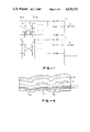
- FIG. 1 depicts a circuit schematic of a memory array in accordance with the invention.
- FIG. 2 depicts a multi-layer composite drawing of a first portion of a memory cell layout in accordance with the invention.
- FIG. 3 depicts a multi-layer composite drawing of a second portion of a memory cell layout in accordance with the invention.
- FIG. 4 depicts a cross-section of a memory cell in accordance with the invention.
- the invention comprises an semiconductor memory array of 4-IGFET (insulated gate field effect transistor) cells.
- the improvement comprising the invention lies in the particular design and organization of the array and cells.
- the four transistors T1, T2, T3 and T4 in each cell of the preferred embodiment are n-channel MOS transistors. Further, the array is intended for use in a CMOS memory device, wherein the peripheral circuitry for the memory includes both p-channel and n-channel transistors.
- the array resides in a large p-well which is formed in an N-substrate.
- the p-well is grounded and the N- substrate is back biased.
- charges induced by alpha particles burying into the p-well are swept into the substrate and away from the capacitive nodes of the memory array.
- Capacitors C1 and C2 are formed by a grounded poly-silicon plate P2 which overlies the cells. In the preferred embodiment, these capacitors account for approximately 60% of the capacitance of each capacitive node N1 and N2 of the cell. In other words, the grounded poly-silicon plate P2 approximately doubles the charge storage capacity of the memory cells without increasing the size of the cells.
- the memory array of the invention provides differential metal bit lines BL and BL for each column, formed on a first layer of patterned metal (labelled M1).
- M1 patterned metal
- differential bit lines provide faster access than single ended bit lines.
- metal bit lines speed memory access considerably compared to poly-silicon bit lines and are simpler to fabricate than poly-silicon-silicide bit lines.
- the preferred embodiment of the invention uses split poly-silicon word lines WL x --one for each access transistor T1 and T2. More importantly, the poly-silicon word lines are paralleled by metal word lines on a second metal layer.
- the metal word lines contact the poly-silicon word lines once every 32 cells.
- the use of metal word lines greatly reduces memory access time compared to the use of poly-silicon word lines because of reduced resistance.
- the use of split poly-silicon word lines is extremely convenient for efficient cell layout (i.e., with a high ratio of cell capacitance to cell area).
- the solution is to use both poly and metal word lines in parallel.
- the preferred embodiment of the invention includes a cell layout which is symmetrical with respect to the split poly-silicon word lines.
- the next consideration is how often to interconnect the poly and metal word lines.
- the goals are to minimize the amount of silicon real estate used and yet to insure that no appreciable access time delay (e.g., an additional 10 percent delay) is caused by the r-c time constant of the poly-silicon word lines.
- interconnection is needed only every 200 to 400 microns.
- cell geometry sized on the order of 10 microns, interconnection is needed only every 20 to 40 cells (i.e., every 20 to 40 columns).
- the metal and poly-silicon word lines are interconnected only every 32 columns.
- the preferred rate of interconnecting the metal and poly word lines using available CMOS technologies may vary from as often as every 8 to as seldom as every 128 columns, depending on the cell width, the poly-silicon resistivity, the width of the poly-silicon word lines, the capacitance of the poly-silicon word lines, and the designer's preferred tradeoff between usage of extra silicon area for interconnections and the access time delay which is attributable to the poly-silicon word lines' resistance.
- FIG. 2 there is shown the layout of four memory cells, one of which is labelled to correspond to the labelling of the circuit shown in FIG. 1.
- the darkest shaded area is the first poly-silicon layer (P1).
- the lightly shaded area represents N+ diffusion.
- the areas where P1 areas cross diffusion areas represent MOS transistors.
- First layer metal M1 bit lines BL and BL run in the column direction.
- Second layer metal M2 lies on top of first layer metal M1 (isolated, of course by silicon dioxide and/or silicon nitride insulatory layer(s)) and is not contacted by the circuitry in the cells.
- First layer poly-silicon P1 forms the split word lines WL and the gates of all the cell transistors T1, T2, T3 and T4.
- Second layer poly-silicon P2 lies on top of the first layer poly-silicon P1 (isolated, of course, by silicon dioxide and/or silicon nitride insulatory layer(s)).
- P2 is grounded by means of periodic connections (VM1P2) to the circuit ground, as will be shown in the discussion of FIG. 3.
- V1P2 periodic connections to the circuit ground, as will be shown in the discussion of FIG. 3.
- P2 connects to two diffusion areas DF1 and DF2 of each cell. These grounded diffusion areas DF1 and DF2 are each shared by two cells (except for certain diffusion areas at the edge of each sub-array of cells (see FIG. 3).
- the second layer poly-silicon P2 is further designed to cover the capacitive nodes of the cells, on which the cells depend for their memory retention properties.
- This P2 layer increases the cell capacitance by providing an AC-grounded (i.e., stable voltage) capacitor plate for the capacitive nodes N1 and N2, and thereby increases the ratio of cell capacitance to cell area.
- the poly-silicon P2 plate also substantially decouples the bit lines from the capacitive nodes of the cells. Only a small fraction of each capacitive node (e.g., the area labelled ACX) is not shielded from the overlying bit line.
- the P1 and P2 poly-silicon layers are separated by an insulator which is approximately 1000 angstroms thick, whereas the gate oxide separating P1 from the transistor channels is approximately 275 to 300 angstroms thick.
- the P2 poly-silicon plate forms a capacitor (see capacitors C1 and C2 in FIG. 1) of approximately 15 femtofarads with each capacitive node in the array. The total capacitance of each capacitive node is approximately 25 femtofarads.
- the thickness of the insulator between P1 and P2 can be varied so as to control the charge storage capacity of the cells. While in general the P2 plate will normally be used to contribute at least 25 percent of the cell's capacitance, considerably higher cell storage capacitance can be achieved by decreasing the thickness of the insulator between P1 and P2.
- the P2 layer also provides some protection against alpha particles impinging on the array at acute (i.e., glancing) angles.
- glancing alpha particles are the hardest to protect against in any IGFET-type memory array because the induced charges tend to be generated in the vicinity of the cell's capacitive node.
- the provision of a grounded P2 layer reduces the danger of soft errors caused by such alpha particles. Note that deeper penetrating alpha particles, which impinge on the semiconductor surface at a more obtuse angle, tend to generate electrical charges in the p-well where they are swept into the N- substrate and away from the capacitive nodes of the cells.
- BC1 areas provide contact between diffusion and P1.
- BC2 areas provide contact between diffusion and P2.
- a further advantage of the cells shown in FIG. 2 are their relatively long length in the bit line direction (e.g., about 19 microns in the preferred embodiment) compared to their width (e.g., about 10 microns), which facilitates the layout of adequate strength word line decoders.
- the memory cells are symmetric with respect to the split poly-silicon P1 word lines.
- FIG. 3 there is shown the portion of the memory array layout where the circuit ground is connected to the P2 plate and to the p-well, and where the M2 word lines are connected to the split poly-silicon P1 word lines.
- M2 is connected to M1 by means of two vias labelled VM1M2. Also, M1 is connected to P1 by means of vias labelled VM1P1. Therefore the M2 word lines are connected to the P1 word lines indirectly through first layer metal M1.
- Metal column line 50 is an M1 line, parallel to the bit lines, which acts as a ground line.
- the M1 column 50 is connected to the grounded p-well by means of a contact VMD in each row (which is formed in the same processing steps as the contacts labelled VMD in FIG. 2.
- THe P2 plate is then connected to M1 by means of vias VM1P2.
- FIG. 4 there is shown a cross-section of a memory cell, as identified by section line 4 in FIG. 2.
- the P2 layer is located so as to provide a significant portion of the memory cell's capacitance.
- the P2 layer also shields the memory cell from the M1 bit lines and is located so as to help absorb alpha particle radiation.
- a memory array in accordance with the invention can be manufactured using well known manufacturing techniques and therefore a process for the manufacture of such a memory device is not described herein.
Abstract
Description
Claims (9)
Priority Applications (1)
| Application Number | Priority Date | Filing Date | Title |
|---|---|---|---|
| US06/699,051 US4679171A (en) | 1985-02-07 | 1985-02-07 | MOS/CMOS memory cell |
Applications Claiming Priority (1)
| Application Number | Priority Date | Filing Date | Title |
|---|---|---|---|
| US06/699,051 US4679171A (en) | 1985-02-07 | 1985-02-07 | MOS/CMOS memory cell |
Publications (1)
| Publication Number | Publication Date |
|---|---|
| US4679171A true US4679171A (en) | 1987-07-07 |
Family
ID=24807731
Family Applications (1)
| Application Number | Title | Priority Date | Filing Date |
|---|---|---|---|
| US06/699,051 Expired - Lifetime US4679171A (en) | 1985-02-07 | 1985-02-07 | MOS/CMOS memory cell |
Country Status (1)
| Country | Link |
|---|---|
| US (1) | US4679171A (en) |
Cited By (30)
| Publication number | Priority date | Publication date | Assignee | Title |
|---|---|---|---|---|
| US4748133A (en) * | 1987-06-26 | 1988-05-31 | Motorola Inc. | Deposition of amorphous silicon for the formation of interlevel dielectrics in semiconductor memory devices |
| US4782465A (en) * | 1983-07-27 | 1988-11-01 | Hitachi, Ltd. | Semiconductor integrated circuit device with memory cells connected to a divided sub-word line |
| US4829351A (en) * | 1987-03-16 | 1989-05-09 | Motorola, Inc. | Polysilicon pattern for a floating gate memory |
| US4835458A (en) * | 1987-11-09 | 1989-05-30 | Intel Corporation | Signature analysis technique for defect characterization of CMOS static RAM cell failures |
| US4849801A (en) * | 1984-11-28 | 1989-07-18 | Hitachi, Ltd. | Semiconductor memory device having increased capacitance for the storing nodes of the memory cells |
| US4853894A (en) * | 1986-07-09 | 1989-08-01 | Hitachi, Ltd. | Static random-access memory having multilevel conductive layer |
| EP0365690A1 (en) * | 1988-05-07 | 1990-05-02 | Seiko Epson Corporation | Semiconductor device and semiconductor memory device |
| DE3939314A1 (en) * | 1988-12-06 | 1990-06-07 | Mitsubishi Electric Corp | Multi-zone semiconductor DRAM - has connection areas with connecting lines on layers, crossing over memory layers |
| US4951112A (en) * | 1987-01-28 | 1990-08-21 | Advanced Micro Devices, Inc. | Triple-poly 4T static ram cell with two independent transistor gates |
| US4984200A (en) * | 1987-11-30 | 1991-01-08 | Hitachi, Ltd. | Semiconductor circuit device having a plurality of SRAM type memory cell arrangement |
| US5043939A (en) * | 1989-06-15 | 1991-08-27 | Bipolar Integrated Technology, Inc. | Soft error immune memory |
| US5045915A (en) * | 1988-11-21 | 1991-09-03 | Nec Corporation | Semiconductor integrated circuit device |
| US5119149A (en) * | 1990-10-22 | 1992-06-02 | Motorola, Inc. | Gate-drain shield reduces gate to drain capacitance |
| EP0499824A1 (en) * | 1991-01-30 | 1992-08-26 | Texas Instruments Incorporated | Stacked capacitor SRAM cell |
| EP0510370A1 (en) * | 1991-03-27 | 1992-10-28 | Fujitsu Limited | Semiconductor memory device having thin film transistor and method of producing the same |
| US5184321A (en) * | 1988-12-06 | 1993-02-02 | Mitsubishi Denki Kabushiki Kaisha | Semiconductor memory device comprising a plurality of memory arrays with improved peripheral circuit location and interconnection arrangement |
| US5239196A (en) * | 1990-02-09 | 1993-08-24 | Shuji Ikeda | SRAM with dual word lines overlapping drive transistor gates |
| US5252848A (en) * | 1992-02-03 | 1993-10-12 | Motorola, Inc. | Low on resistance field effect transistor |
| US5254870A (en) * | 1988-05-07 | 1993-10-19 | Seiko Epson Corporation | Static random access memory having memory cells with electric field shielding for cell load resistances |
| US5300814A (en) * | 1991-07-18 | 1994-04-05 | Matsushita Electric Industrial Co., Ltd. | Semiconductor device having a semiconductor substrate with reduced step between memory cells |
| US5324961A (en) * | 1991-01-30 | 1994-06-28 | Texas Instruments Incorporated | Stacked capacitor SRAM cell |
| US5377139A (en) * | 1992-12-11 | 1994-12-27 | Motorola, Inc. | Process forming an integrated circuit |
| US5536674A (en) * | 1992-12-11 | 1996-07-16 | Motorola, Inc. | Process for forming a static-random-access memory cell |
| US5698872A (en) * | 1989-09-13 | 1997-12-16 | Kabushiki Kaisha Toshiba | Semiconductor memory wherein metallic interconnection layer is applied with the same potential as word line and is connected to word line in regions other than memory cells |
| US5874332A (en) * | 1991-06-07 | 1999-02-23 | Fujitsu Limited | Semiconductor memory device having a memory cell capacitor and a fabrication process thereof |
| US6001681A (en) * | 1999-01-19 | 1999-12-14 | Taiwan Semiconductor Manufacturing Company, Ltd. | Method to reduce the depth of a buried contact trench by using a thin split polysilicon thickness |
| DE4408758C2 (en) * | 1993-03-15 | 2003-02-27 | Hyundai Electronics Ind | Word line structure in a semiconductor memory device |
| US20070032065A1 (en) * | 2005-07-26 | 2007-02-08 | Porter Howard L | Alpha-particle-tolerant semiconductor die systems, devices, components and methods for optimizing clock rates and minimizing die size |
| US20070050599A1 (en) * | 2005-07-26 | 2007-03-01 | Porter Howard L | Determining the placement of semiconductor components on an integrated circuit |
| US20070131988A1 (en) * | 2005-12-12 | 2007-06-14 | Taiwan Semiconductor Manufacturing Co., Ltd. | CMOS image sensor devices and fabrication method thereof |
Citations (4)
| Publication number | Priority date | Publication date | Assignee | Title |
|---|---|---|---|---|
| US4234889A (en) * | 1977-05-31 | 1980-11-18 | Texas Instruments Incorporated | Metal-to-moat contacts in N-channel silicon gate integrated circuits using discrete second-level polycrystalline silicon |
| JPS56107575A (en) * | 1980-01-29 | 1981-08-26 | Nec Corp | Manufacture of semicondutor device |
| JPS58199557A (en) * | 1982-05-15 | 1983-11-19 | Toshiba Corp | Dynamic memory device |
| US4481524A (en) * | 1979-01-23 | 1984-11-06 | Nippon Electric Co., Ltd. | Semiconductor memory device having stacked polycrystalline silicon layers |
-
1985
- 1985-02-07 US US06/699,051 patent/US4679171A/en not_active Expired - Lifetime
Patent Citations (4)
| Publication number | Priority date | Publication date | Assignee | Title |
|---|---|---|---|---|
| US4234889A (en) * | 1977-05-31 | 1980-11-18 | Texas Instruments Incorporated | Metal-to-moat contacts in N-channel silicon gate integrated circuits using discrete second-level polycrystalline silicon |
| US4481524A (en) * | 1979-01-23 | 1984-11-06 | Nippon Electric Co., Ltd. | Semiconductor memory device having stacked polycrystalline silicon layers |
| JPS56107575A (en) * | 1980-01-29 | 1981-08-26 | Nec Corp | Manufacture of semicondutor device |
| JPS58199557A (en) * | 1982-05-15 | 1983-11-19 | Toshiba Corp | Dynamic memory device |
Cited By (41)
| Publication number | Priority date | Publication date | Assignee | Title |
|---|---|---|---|---|
| US4782465A (en) * | 1983-07-27 | 1988-11-01 | Hitachi, Ltd. | Semiconductor integrated circuit device with memory cells connected to a divided sub-word line |
| US4849801A (en) * | 1984-11-28 | 1989-07-18 | Hitachi, Ltd. | Semiconductor memory device having increased capacitance for the storing nodes of the memory cells |
| US4853894A (en) * | 1986-07-09 | 1989-08-01 | Hitachi, Ltd. | Static random-access memory having multilevel conductive layer |
| US4951112A (en) * | 1987-01-28 | 1990-08-21 | Advanced Micro Devices, Inc. | Triple-poly 4T static ram cell with two independent transistor gates |
| US4829351A (en) * | 1987-03-16 | 1989-05-09 | Motorola, Inc. | Polysilicon pattern for a floating gate memory |
| US4748133A (en) * | 1987-06-26 | 1988-05-31 | Motorola Inc. | Deposition of amorphous silicon for the formation of interlevel dielectrics in semiconductor memory devices |
| US4835458A (en) * | 1987-11-09 | 1989-05-30 | Intel Corporation | Signature analysis technique for defect characterization of CMOS static RAM cell failures |
| US4984200A (en) * | 1987-11-30 | 1991-01-08 | Hitachi, Ltd. | Semiconductor circuit device having a plurality of SRAM type memory cell arrangement |
| EP0365690A1 (en) * | 1988-05-07 | 1990-05-02 | Seiko Epson Corporation | Semiconductor device and semiconductor memory device |
| EP0365690A4 (en) * | 1988-05-07 | 1991-11-27 | Seiko Epson Corporation | Semiconductor device and semiconductor memory device |
| US5254870A (en) * | 1988-05-07 | 1993-10-19 | Seiko Epson Corporation | Static random access memory having memory cells with electric field shielding for cell load resistances |
| US5045915A (en) * | 1988-11-21 | 1991-09-03 | Nec Corporation | Semiconductor integrated circuit device |
| DE3939314A1 (en) * | 1988-12-06 | 1990-06-07 | Mitsubishi Electric Corp | Multi-zone semiconductor DRAM - has connection areas with connecting lines on layers, crossing over memory layers |
| US5184321A (en) * | 1988-12-06 | 1993-02-02 | Mitsubishi Denki Kabushiki Kaisha | Semiconductor memory device comprising a plurality of memory arrays with improved peripheral circuit location and interconnection arrangement |
| US5043939A (en) * | 1989-06-15 | 1991-08-27 | Bipolar Integrated Technology, Inc. | Soft error immune memory |
| US5698872A (en) * | 1989-09-13 | 1997-12-16 | Kabushiki Kaisha Toshiba | Semiconductor memory wherein metallic interconnection layer is applied with the same potential as word line and is connected to word line in regions other than memory cells |
| US5239196A (en) * | 1990-02-09 | 1993-08-24 | Shuji Ikeda | SRAM with dual word lines overlapping drive transistor gates |
| US5652457A (en) * | 1990-02-09 | 1997-07-29 | Hitachi, Ltd. | Semiconductor integrated circuit device and process for fabricating the same |
| US5767554A (en) * | 1990-02-09 | 1998-06-16 | Hitachi, Ltd. | Semiconductor integrated circuit device and process for fabricating the same |
| US5119149A (en) * | 1990-10-22 | 1992-06-02 | Motorola, Inc. | Gate-drain shield reduces gate to drain capacitance |
| EP0499824A1 (en) * | 1991-01-30 | 1992-08-26 | Texas Instruments Incorporated | Stacked capacitor SRAM cell |
| US5324961A (en) * | 1991-01-30 | 1994-06-28 | Texas Instruments Incorporated | Stacked capacitor SRAM cell |
| EP0510370A1 (en) * | 1991-03-27 | 1992-10-28 | Fujitsu Limited | Semiconductor memory device having thin film transistor and method of producing the same |
| US5594267A (en) * | 1991-03-27 | 1997-01-14 | Fujitsu Limited | Semiconductor memory device having thin film transistor and method of producing the same |
| US5874332A (en) * | 1991-06-07 | 1999-02-23 | Fujitsu Limited | Semiconductor memory device having a memory cell capacitor and a fabrication process thereof |
| US6066871A (en) * | 1991-06-07 | 2000-05-23 | Fujitsu Limited | Semiconductor memory device having a memory cell capacitor and a fabrication process thereof |
| US5300814A (en) * | 1991-07-18 | 1994-04-05 | Matsushita Electric Industrial Co., Ltd. | Semiconductor device having a semiconductor substrate with reduced step between memory cells |
| US5252848A (en) * | 1992-02-03 | 1993-10-12 | Motorola, Inc. | Low on resistance field effect transistor |
| US5485420A (en) * | 1992-12-11 | 1996-01-16 | Motorola, Inc. | Static-random-access memory cell and an integrated circuit having a static-random-access memory cell |
| US5377139A (en) * | 1992-12-11 | 1994-12-27 | Motorola, Inc. | Process forming an integrated circuit |
| US5739564A (en) * | 1992-12-11 | 1998-04-14 | Motorola, Inc. | Semiconductor device having a static-random-access memory cell |
| US5536674A (en) * | 1992-12-11 | 1996-07-16 | Motorola, Inc. | Process for forming a static-random-access memory cell |
| DE4408758C2 (en) * | 1993-03-15 | 2003-02-27 | Hyundai Electronics Ind | Word line structure in a semiconductor memory device |
| US6001681A (en) * | 1999-01-19 | 1999-12-14 | Taiwan Semiconductor Manufacturing Company, Ltd. | Method to reduce the depth of a buried contact trench by using a thin split polysilicon thickness |
| US20070032065A1 (en) * | 2005-07-26 | 2007-02-08 | Porter Howard L | Alpha-particle-tolerant semiconductor die systems, devices, components and methods for optimizing clock rates and minimizing die size |
| US20070050599A1 (en) * | 2005-07-26 | 2007-03-01 | Porter Howard L | Determining the placement of semiconductor components on an integrated circuit |
| US7386824B2 (en) * | 2005-07-26 | 2008-06-10 | Avago Technologies General Ip Pte Ltd | Determining the placement of semiconductor components on an integrated circuit |
| US20080230900A1 (en) * | 2005-07-26 | 2008-09-25 | Porter Howard L | Determining the placement of semiconductor components on an integrated circuit |
| US7451418B2 (en) | 2005-07-26 | 2008-11-11 | Avago Technologies Enterprise IP (Singapore) Pte. Ltd. | Alpha-particle-tolerant semiconductor die systems, devices, components and methods for optimizing clock rates and minimizing die size |
| US7915742B2 (en) | 2005-07-26 | 2011-03-29 | Avago Technologies General Ip (Singapore) Pte. Ltd. | Determining the placement of semiconductor components on an integrated circuit |
| US20070131988A1 (en) * | 2005-12-12 | 2007-06-14 | Taiwan Semiconductor Manufacturing Co., Ltd. | CMOS image sensor devices and fabrication method thereof |
Similar Documents
| Publication | Publication Date | Title |
|---|---|---|
| US4679171A (en) | MOS/CMOS memory cell | |
| US6057188A (en) | Trench capacitor structures | |
| EP0452648B1 (en) | Stacked bit line architecture for high density cross-point memory cell array | |
| US5432365A (en) | Semiconductor memory device | |
| US6133597A (en) | Biasing an integrated circuit well with a transistor electrode | |
| US5175605A (en) | Single event upset hardening circuits, devices and methods | |
| US5521860A (en) | CMOS static memory | |
| US4849801A (en) | Semiconductor memory device having increased capacitance for the storing nodes of the memory cells | |
| CN1139130C (en) | CMOS static random access memory devices | |
| EP1083604A2 (en) | Radiation hardened semiconductor memory | |
| US6600186B1 (en) | Process technology architecture of embedded DRAM | |
| US6380598B1 (en) | Radiation hardened semiconductor memory | |
| US4763178A (en) | Semiconductor memory device | |
| JP2634163B2 (en) | Semiconductor storage device | |
| Inoue et al. | A 16-Mbit DRAM with a relaxed sense-amplifier-pitch open-bit-line architecture | |
| US4635085A (en) | Semiconductor memory device | |
| US5334863A (en) | Semiconductor memory device having a meshlike grounding wiring | |
| US5917247A (en) | Static type memory cell structure with parasitic capacitor | |
| US6730947B2 (en) | Semiconductor integrated circuit apparatus having an periphery impurity layer | |
| JP2003060071A (en) | Semiconductor integrated circuit device | |
| US4825268A (en) | Semiconductor memory device | |
| KR20040069665A (en) | SRAM cell and method of manufacturing the same | |
| EP0329100B1 (en) | Semiconductor device comprising a logic circuit and a memory | |
| US20010042926A1 (en) | Semiconductor memory device | |
| GB2113910A (en) | One-transistor dynamic ram cells |
Legal Events
| Date | Code | Title | Description |
|---|---|---|---|
| AS | Assignment |
Owner name: VISIC INC. SAN JOSE CALIFORNIA A CORP OF CA Free format text: ASSIGNMENT OF ASSIGNORS INTEREST.;ASSIGNORS:KARP, JOEL ALLEN;LOGWOOD, DENNIS J.;HAG, MOHAMMED E. U.;AND OTHERS;REEL/FRAME:004412/0511 Effective date: 19850205 |
|
| STCF | Information on status: patent grant |
Free format text: PATENTED CASE |
|
| FEPP | Fee payment procedure |
Free format text: PAT HLDR NO LONGER CLAIMS SMALL ENT STAT AS INDIV INVENTOR (ORIGINAL EVENT CODE: LSM1); ENTITY STATUS OF PATENT OWNER: LARGE ENTITY |
|
| FPAY | Fee payment |
Year of fee payment: 4 |
|
| AS | Assignment |
Owner name: VISIC, INC., LIQUIDATING TRUST REPRESENTED BY MOHA Free format text: ASSIGNMENT OF ASSIGNORS INTEREST.;ASSIGNOR:VLSI TECHNOLOGY, INC.;REEL/FRAME:005699/0575 Effective date: 19901214 |
|
| AS | Assignment |
Owner name: POONJA, MOHAMED UNDER THE VISIC, INC. LIQUIDATING Free format text: ASSIGNMENT OF ASSIGNORS INTEREST.;ASSIGNOR:VISIC, INC., A CA CORP.;REEL/FRAME:006014/0062 Effective date: 19901217 |
|
| AS | Assignment |
Owner name: POONJA, MOHAMED, AS TRUSTEE UNDER THE VISIC, INC. Free format text: ASSIGNMENT OF ASSIGNORS INTEREST.;ASSIGNOR:VISIC, INC., A CORP. OF CA;REEL/FRAME:006113/0835 Effective date: 19911018 Owner name: AMERICAN TELEPHONE AND TELEGRAPH COMPANY, A CORP. Free format text: ASSIGNMENT OF ASSIGNORS INTEREST.;ASSIGNOR:POONJI, MOHAMED, AS TRUSTEE UNDER THE VISIC, INC. LIQUIDATING TRUST AGREEMENT DATED DECEMBER 18, 1990;REEL/FRAME:006113/0828 Effective date: 19911018 |
|
| FEPP | Fee payment procedure |
Free format text: PAYOR NUMBER ASSIGNED (ORIGINAL EVENT CODE: ASPN); ENTITY STATUS OF PATENT OWNER: LARGE ENTITY |
|
| FPAY | Fee payment |
Year of fee payment: 8 |
|
| FEPP | Fee payment procedure |
Free format text: PAYER NUMBER DE-ASSIGNED (ORIGINAL EVENT CODE: RMPN); ENTITY STATUS OF PATENT OWNER: LARGE ENTITY Free format text: PAYOR NUMBER ASSIGNED (ORIGINAL EVENT CODE: ASPN); ENTITY STATUS OF PATENT OWNER: LARGE ENTITY |
|
| FPAY | Fee payment |
Year of fee payment: 12 |