US4699805A - Process and apparatus for the low pressure chemical vapor deposition of thin films - Google Patents
Process and apparatus for the low pressure chemical vapor deposition of thin films Download PDFInfo
- Publication number
- US4699805A US4699805A US06/881,988 US88198886A US4699805A US 4699805 A US4699805 A US 4699805A US 88198886 A US88198886 A US 88198886A US 4699805 A US4699805 A US 4699805A
- Authority
- US
- United States
- Prior art keywords
- reactant
- reaction chamber
- injector tube
- end cap
- chamber
- Prior art date
- Legal status (The legal status is an assumption and is not a legal conclusion. Google has not performed a legal analysis and makes no representation as to the accuracy of the status listed.)
- Expired - Lifetime
Links
- 238000000034 method Methods 0.000 title claims abstract description 31
- 230000008569 process Effects 0.000 title claims abstract description 28
- 238000004518 low pressure chemical vapour deposition Methods 0.000 title claims abstract description 25
- 239000010409 thin film Substances 0.000 title claims description 11
- 238000006243 chemical reaction Methods 0.000 claims abstract description 78
- 238000000151 deposition Methods 0.000 claims abstract description 67
- 230000008021 deposition Effects 0.000 claims abstract description 66
- 239000000376 reactant Substances 0.000 claims abstract description 61
- 238000002347 injection Methods 0.000 claims abstract description 42
- 239000007924 injection Substances 0.000 claims abstract description 42
- 239000010408 film Substances 0.000 claims description 49
- 230000008878 coupling Effects 0.000 claims description 15
- 238000010168 coupling process Methods 0.000 claims description 15
- 238000005859 coupling reaction Methods 0.000 claims description 15
- 150000001875 compounds Chemical class 0.000 claims description 11
- 238000005086 pumping Methods 0.000 claims description 9
- 238000010438 heat treatment Methods 0.000 claims description 6
- 150000004820 halides Chemical class 0.000 claims description 4
- 229910001507 metal halide Inorganic materials 0.000 claims description 2
- 150000005309 metal halides Chemical class 0.000 claims description 2
- 238000007789 sealing Methods 0.000 claims 3
- 229910000765 intermetallic Inorganic materials 0.000 claims 1
- 238000007493 shaping process Methods 0.000 claims 1
- 239000000758 substrate Substances 0.000 claims 1
- 239000000463 material Substances 0.000 description 30
- 239000007789 gas Substances 0.000 description 27
- VYPSYNLAJGMNEJ-UHFFFAOYSA-N Silicium dioxide Chemical compound O=[Si]=O VYPSYNLAJGMNEJ-UHFFFAOYSA-N 0.000 description 18
- 239000010453 quartz Substances 0.000 description 17
- 235000012431 wafers Nutrition 0.000 description 16
- 239000004065 semiconductor Substances 0.000 description 11
- 229910003074 TiCl4 Inorganic materials 0.000 description 8
- 239000006227 byproduct Substances 0.000 description 8
- 238000009792 diffusion process Methods 0.000 description 8
- XJDNKRIXUMDJCW-UHFFFAOYSA-J titanium tetrachloride Chemical compound Cl[Ti](Cl)(Cl)Cl XJDNKRIXUMDJCW-UHFFFAOYSA-J 0.000 description 8
- 229910001220 stainless steel Inorganic materials 0.000 description 6
- 239000010935 stainless steel Substances 0.000 description 6
- QGZKDVFQNNGYKY-UHFFFAOYSA-N Ammonia Chemical compound N QGZKDVFQNNGYKY-UHFFFAOYSA-N 0.000 description 5
- BLRPTPMANUNPDV-UHFFFAOYSA-N Silane Chemical compound [SiH4] BLRPTPMANUNPDV-UHFFFAOYSA-N 0.000 description 5
- 239000012159 carrier gas Substances 0.000 description 5
- 239000001257 hydrogen Substances 0.000 description 5
- 229910052739 hydrogen Inorganic materials 0.000 description 5
- WQJQOUPTWCFRMM-UHFFFAOYSA-N tungsten disilicide Chemical compound [Si]#[W]#[Si] WQJQOUPTWCFRMM-UHFFFAOYSA-N 0.000 description 5
- 229910021342 tungsten silicide Inorganic materials 0.000 description 5
- XKRFYHLGVUSROY-UHFFFAOYSA-N Argon Chemical compound [Ar] XKRFYHLGVUSROY-UHFFFAOYSA-N 0.000 description 4
- UFHFLCQGNIYNRP-UHFFFAOYSA-N Hydrogen Chemical compound [H][H] UFHFLCQGNIYNRP-UHFFFAOYSA-N 0.000 description 4
- ATJFFYVFTNAWJD-UHFFFAOYSA-N Tin Chemical compound [Sn] ATJFFYVFTNAWJD-UHFFFAOYSA-N 0.000 description 4
- RTAQQCXQSZGOHL-UHFFFAOYSA-N Titanium Chemical compound [Ti] RTAQQCXQSZGOHL-UHFFFAOYSA-N 0.000 description 4
- 229910000039 hydrogen halide Inorganic materials 0.000 description 4
- 239000012433 hydrogen halide Substances 0.000 description 4
- 229910052751 metal Inorganic materials 0.000 description 4
- 239000002184 metal Substances 0.000 description 4
- 229910021420 polycrystalline silicon Inorganic materials 0.000 description 4
- 229910052719 titanium Inorganic materials 0.000 description 4
- 239000010936 titanium Substances 0.000 description 4
- XUIMIQQOPSSXEZ-UHFFFAOYSA-N Silicon Chemical compound [Si] XUIMIQQOPSSXEZ-UHFFFAOYSA-N 0.000 description 3
- 229910008814 WSi2 Inorganic materials 0.000 description 3
- 230000006835 compression Effects 0.000 description 3
- 238000007906 compression Methods 0.000 description 3
- 239000012535 impurity Substances 0.000 description 3
- 238000012986 modification Methods 0.000 description 3
- 230000004048 modification Effects 0.000 description 3
- 230000000877 morphologic effect Effects 0.000 description 3
- 229910000069 nitrogen hydride Inorganic materials 0.000 description 3
- 230000000704 physical effect Effects 0.000 description 3
- 238000009428 plumbing Methods 0.000 description 3
- 239000003870 refractory metal Substances 0.000 description 3
- 229910052710 silicon Inorganic materials 0.000 description 3
- 239000010703 silicon Substances 0.000 description 3
- 238000011144 upstream manufacturing Methods 0.000 description 3
- IJGRMHOSHXDMSA-UHFFFAOYSA-N Atomic nitrogen Chemical compound N#N IJGRMHOSHXDMSA-UHFFFAOYSA-N 0.000 description 2
- QYEXBYZXHDUPRC-UHFFFAOYSA-N B#[Ti]#B Chemical group B#[Ti]#B QYEXBYZXHDUPRC-UHFFFAOYSA-N 0.000 description 2
- BQCADISMDOOEFD-UHFFFAOYSA-N Silver Chemical compound [Ag] BQCADISMDOOEFD-UHFFFAOYSA-N 0.000 description 2
- 230000002411 adverse Effects 0.000 description 2
- 229910052782 aluminium Inorganic materials 0.000 description 2
- XAGFODPZIPBFFR-UHFFFAOYSA-N aluminium Chemical compound [Al] XAGFODPZIPBFFR-UHFFFAOYSA-N 0.000 description 2
- 229910052786 argon Inorganic materials 0.000 description 2
- 230000015572 biosynthetic process Effects 0.000 description 2
- 238000005229 chemical vapour deposition Methods 0.000 description 2
- 230000000694 effects Effects 0.000 description 2
- 239000011521 glass Substances 0.000 description 2
- 150000002431 hydrogen Chemical class 0.000 description 2
- 239000011261 inert gas Substances 0.000 description 2
- 238000003780 insertion Methods 0.000 description 2
- 230000037431 insertion Effects 0.000 description 2
- 238000004519 manufacturing process Methods 0.000 description 2
- 239000000203 mixture Substances 0.000 description 2
- 238000009828 non-uniform distribution Methods 0.000 description 2
- 229910052709 silver Inorganic materials 0.000 description 2
- 239000004332 silver Substances 0.000 description 2
- WFKWXMTUELFFGS-UHFFFAOYSA-N tungsten Chemical compound [W] WFKWXMTUELFFGS-UHFFFAOYSA-N 0.000 description 2
- 229910052721 tungsten Inorganic materials 0.000 description 2
- 239000010937 tungsten Substances 0.000 description 2
- 238000009827 uniform distribution Methods 0.000 description 2
- -1 B2 H6 Chemical compound 0.000 description 1
- 229910015844 BCl3 Inorganic materials 0.000 description 1
- ZOXJGFHDIHLPTG-UHFFFAOYSA-N Boron Chemical compound [B] ZOXJGFHDIHLPTG-UHFFFAOYSA-N 0.000 description 1
- OKTJSMMVPCPJKN-UHFFFAOYSA-N Carbon Chemical compound [C] OKTJSMMVPCPJKN-UHFFFAOYSA-N 0.000 description 1
- 229910052581 Si3N4 Inorganic materials 0.000 description 1
- 229910033181 TiB2 Inorganic materials 0.000 description 1
- NRTOMJZYCJJWKI-UHFFFAOYSA-N Titanium nitride Chemical compound [Ti]#N NRTOMJZYCJJWKI-UHFFFAOYSA-N 0.000 description 1
- HGTYEBNTDPDGIC-UHFFFAOYSA-N [N].[Au] Chemical compound [N].[Au] HGTYEBNTDPDGIC-UHFFFAOYSA-N 0.000 description 1
- 229910021529 ammonia Inorganic materials 0.000 description 1
- 238000013459 approach Methods 0.000 description 1
- XKRFYHLGVUSROY-AHCXROLUSA-N argon-36 Chemical compound [36Ar] XKRFYHLGVUSROY-AHCXROLUSA-N 0.000 description 1
- QVGXLLKOCUKJST-UHFFFAOYSA-N atomic oxygen Chemical compound [O] QVGXLLKOCUKJST-UHFFFAOYSA-N 0.000 description 1
- 230000004888 barrier function Effects 0.000 description 1
- 229910052796 boron Inorganic materials 0.000 description 1
- 229910052799 carbon Inorganic materials 0.000 description 1
- 230000015556 catabolic process Effects 0.000 description 1
- 239000000470 constituent Substances 0.000 description 1
- 239000000356 contaminant Substances 0.000 description 1
- 238000011109 contamination Methods 0.000 description 1
- 238000001816 cooling Methods 0.000 description 1
- 238000012864 cross contamination Methods 0.000 description 1
- 238000006731 degradation reaction Methods 0.000 description 1
- 238000005137 deposition process Methods 0.000 description 1
- 238000013461 design Methods 0.000 description 1
- 238000009826 distribution Methods 0.000 description 1
- 230000005484 gravity Effects 0.000 description 1
- 150000004678 hydrides Chemical class 0.000 description 1
- 229910001502 inorganic halide Inorganic materials 0.000 description 1
- 229910010276 inorganic hydride Inorganic materials 0.000 description 1
- 238000001465 metallisation Methods 0.000 description 1
- 150000002739 metals Chemical class 0.000 description 1
- 238000012544 monitoring process Methods 0.000 description 1
- 229910052757 nitrogen Inorganic materials 0.000 description 1
- 238000005457 optimization Methods 0.000 description 1
- 239000001301 oxygen Substances 0.000 description 1
- 229910052760 oxygen Inorganic materials 0.000 description 1
- 238000012545 processing Methods 0.000 description 1
- 239000011253 protective coating Substances 0.000 description 1
- 230000001681 protective effect Effects 0.000 description 1
- 238000010926 purge Methods 0.000 description 1
- 230000001105 regulatory effect Effects 0.000 description 1
- 238000012552 review Methods 0.000 description 1
- 238000007086 side reaction Methods 0.000 description 1
- HQVNEWCFYHHQES-UHFFFAOYSA-N silicon nitride Chemical compound N12[Si]34N5[Si]62N3[Si]51N64 HQVNEWCFYHHQES-UHFFFAOYSA-N 0.000 description 1
- 229910052814 silicon oxide Inorganic materials 0.000 description 1
- 125000006850 spacer group Chemical group 0.000 description 1
- 239000000126 substance Substances 0.000 description 1
- 229910021341 titanium silicide Inorganic materials 0.000 description 1
- FAQYAMRNWDIXMY-UHFFFAOYSA-N trichloroborane Chemical compound ClB(Cl)Cl FAQYAMRNWDIXMY-UHFFFAOYSA-N 0.000 description 1
- XLYOFNOQVPJJNP-UHFFFAOYSA-N water Substances O XLYOFNOQVPJJNP-UHFFFAOYSA-N 0.000 description 1
Images


Classifications
-
- C—CHEMISTRY; METALLURGY
- C23—COATING METALLIC MATERIAL; COATING MATERIAL WITH METALLIC MATERIAL; CHEMICAL SURFACE TREATMENT; DIFFUSION TREATMENT OF METALLIC MATERIAL; COATING BY VACUUM EVAPORATION, BY SPUTTERING, BY ION IMPLANTATION OR BY CHEMICAL VAPOUR DEPOSITION, IN GENERAL; INHIBITING CORROSION OF METALLIC MATERIAL OR INCRUSTATION IN GENERAL
- C23C—COATING METALLIC MATERIAL; COATING MATERIAL WITH METALLIC MATERIAL; SURFACE TREATMENT OF METALLIC MATERIAL BY DIFFUSION INTO THE SURFACE, BY CHEMICAL CONVERSION OR SUBSTITUTION; COATING BY VACUUM EVAPORATION, BY SPUTTERING, BY ION IMPLANTATION OR BY CHEMICAL VAPOUR DEPOSITION, IN GENERAL
- C23C16/00—Chemical coating by decomposition of gaseous compounds, without leaving reaction products of surface material in the coating, i.e. chemical vapour deposition [CVD] processes
- C23C16/44—Chemical coating by decomposition of gaseous compounds, without leaving reaction products of surface material in the coating, i.e. chemical vapour deposition [CVD] processes characterised by the method of coating
- C23C16/455—Chemical coating by decomposition of gaseous compounds, without leaving reaction products of surface material in the coating, i.e. chemical vapour deposition [CVD] processes characterised by the method of coating characterised by the method used for introducing gases into reaction chamber or for modifying gas flows in reaction chamber
- C23C16/45561—Gas plumbing upstream of the reaction chamber
-
- C—CHEMISTRY; METALLURGY
- C23—COATING METALLIC MATERIAL; COATING MATERIAL WITH METALLIC MATERIAL; CHEMICAL SURFACE TREATMENT; DIFFUSION TREATMENT OF METALLIC MATERIAL; COATING BY VACUUM EVAPORATION, BY SPUTTERING, BY ION IMPLANTATION OR BY CHEMICAL VAPOUR DEPOSITION, IN GENERAL; INHIBITING CORROSION OF METALLIC MATERIAL OR INCRUSTATION IN GENERAL
- C23C—COATING METALLIC MATERIAL; COATING MATERIAL WITH METALLIC MATERIAL; SURFACE TREATMENT OF METALLIC MATERIAL BY DIFFUSION INTO THE SURFACE, BY CHEMICAL CONVERSION OR SUBSTITUTION; COATING BY VACUUM EVAPORATION, BY SPUTTERING, BY ION IMPLANTATION OR BY CHEMICAL VAPOUR DEPOSITION, IN GENERAL
- C23C16/00—Chemical coating by decomposition of gaseous compounds, without leaving reaction products of surface material in the coating, i.e. chemical vapour deposition [CVD] processes
- C23C16/44—Chemical coating by decomposition of gaseous compounds, without leaving reaction products of surface material in the coating, i.e. chemical vapour deposition [CVD] processes characterised by the method of coating
- C23C16/455—Chemical coating by decomposition of gaseous compounds, without leaving reaction products of surface material in the coating, i.e. chemical vapour deposition [CVD] processes characterised by the method of coating characterised by the method used for introducing gases into reaction chamber or for modifying gas flows in reaction chamber
- C23C16/45563—Gas nozzles
- C23C16/45578—Elongated nozzles, tubes with holes
Definitions
- This invention relates generally to a process and apparatus for the low pressure chemical vapor deposition of thin films, and more specifically to process and apparatus for the deposition of metallic films.
- Low pressure chemical vapor deposition is utilized for the formation of various thin films.
- Several of these films are essential in the fabrication of semiconductor devices including polycrystalline silicon, silicon oxide, and silicon nitride. More recently, interest has been generated in the LPCVD of refractory metallic films such as selective tungsten, tungsten silicide, titanium silicide, titanium nitride, and titanium boride. As applied to the electronics industry, these refractory metallic films are useful as improved gate electrodes and interconnections on MOS devices, contact enhancements to semiconductor materials, metallization of Schottky devices, diffusion barriers, and the like. In other industries the refractory metallic films are utilized to form hard protective coatings for tools, dies, and other types of machinery benefiting from such refractory surfaces.
- the source gases for these binary metallic compounds nominally consist of a semivolatile metal source material such as WF 6 or TiCl 4 and the volatile hydride or halide of an inorganic source material such as SiH 4 , NH 3 , B 2 H 6 , or BCl 3 and H 2 .
- the deposition occurs through the metathetical reaction between the metal halide and inorganic hydride or halide to deposit a refractory metal film and liberate a hydrogen halide.
- tungsten silicide and titanium boride are deposited in accordance with the following reactions. For the deposition of tungsten silicide
- the binary metallic films formed by chemical vapor deposition and specifically by low pressure chemical vapor deposition tend to be uniform and to have very low concentrations of unwanted impurities.
- the stoichimetric uniformity results from the fact that the elemental composition of CVD films is strongly influenced by free energies of formation of compounds for specific stoichiometric values.
- the low concentration of unwanted impurities results from the fact that, during deposition, impurities such as oxygen, carbon, and other trace metals are conducted away from the deposition surface by volatile reaction by-products diffusing away from this surface.
- films deposited by LPCVD tend to be conformal and to yield excellent step coverage.
- polycrystalline silicon is deposited on semiconductor wafers by loading multiple wafer boats into a tubular quartz reactor, evacuating the reactor tube, heating the tube to the desired temperature, and injecting source gases to obtain a uniform deposit across each wafer and from wafer to wafer.
- the deposition of refractory metals and other materials which are deposited from high molecular weight source materials is not as simple, however, as the deposition of polycrystalline silicon. This simplistic approach is not adequate to obtain uniform film thickness from wafer to wafer.
- the major film uniformity problems arise as a result of two factors: (1) The generation of reaction byproducts down the boat; and (2) The retardation of the diffusion rate of the high molecular weight source material as compared to lower molecular weight materials.
- the tungsten silicide is being depleted by the reaction
- the mean free path between molecular collisions approximates the geometries found in a typical LPCVD reactor.
- the diffusion rate of gases thus plays a primary role in their transport; and, therefore, the rate of their transport is approximately proportional to the inverse square root of their molecular masses.
- SiH 4 diffuses about three times as fast as WF 6 .
- Lighter by-product gases such as HF and H 2 diffuse at even higher rates. The result of this disparity in diffusion rates is a non-uniform distribution of reactants along the reaction chamber; the high molecular weight reactant builds up in concentration near the input end in contrast to locations further along the reaction chamber.
- the seal between the reactor tube and the end caps which enclose the ends of the tube be undisturbed once the system is placed in operation. This includes leaving the seals undisturbed when the composition or type of film deposited in the reactor is changed.
- a reaction chamber which has first and second ends enclosed by first and second end caps, respectively.
- a generally U-shaped injection tube including input and output ends coupled through the first end cap is positioned within the reaction chamber.
- the injection tube includes a plurality of injection holes which are positioned centrally near the bottom of the reaction chamber.
- a deposition surface is inserted into the reaction chamber through the second end of the tube to position the surface generally proximate to and over the plurality of injection holes.
- the pressure in the reaction chamber is reduced to the desired reaction pressure and the deposition surface is heated to a predetermined reaction temperature.
- a source of at least one high molecular weight reactant compound is coupled to the input of the injection tube.
- the output of the injection tube is coupled to a vacuum pump and the high molecular weight reactant is pumped through the injection tube, dispersing a desired amount of the reactant through the plurality of injection holes into the reaction chamber.
- the reactant compound is reacted at the heated deposition surface to form the desired thin film.
- the remainder of the higher molecular weight reactant is exhausted from the output end of the injection tube.
- reaction by-products and unreacted source materials are exhausted from the reaction chamber into the vacuum pump.
- the deposition surface with the film thereon is allowed to cool before opening the chamber and exposing the film to the ambient.
- FIG. 1 schematically illustrates deposition apparatus in accordance with the invention
- FIG. 2 illustrates an injector tube in accordance with the invention
- FIGS. 3 and 4 illustrate positioning of injector tubes relative to a deposition surface and a feedthrough plate, respectively.
- FIGS. 5 and 6 illustrate, in cross-section and perspective views, respectively, an end plate and feedthrough in accordance with a preferred embodiment of the invention.
- FIG. 1 schematically illustrates apparatus 10, in accordance with the invention, for the low pressure chemical vapor deposition of thin films, and especially metallic films deposited from high molecular weight reactants.
- the term "metallic" is used to refer to compounds in which one or more of the constituents is a metal.
- the apparatus is especially useful when one or more of the reactants has a molecular weight greater than about 50, and especially for those reactants having a molecular weight greater than about 100. The molecular weight, of course, is measured in atomic mass units. The apparatus can however, be used with other lower molecular weight reactants, but there is less need for the invention with such lower molecular weight reactants.
- a key element in the invention is a generally U-shaped injection tube 12 which provides for the desired distribution of the high molecular weight reactants along the length of the reaction chamber. The U-shaped injection tube is described in more detail below.
- Apparatus 10 can be, for example, a continuously operating furnace, constructed to provide extremely precise temperature, as is widely used in the semiconductor industry.
- LPCVD reactor 10 includes a tubular reaction chamber 14 which is preferably an elongate, cylindrically shaped quartz tube. Electric coils 16 wound around the outside of tube 14 provide the precise temperature control.
- the two ends of the elongate tube 14 are enclosed by end caps 20, 22.
- Attached to end cap 20 is a readily removable feedthrough plate assembly 24 with a plurality of connections for flexible tubes for passing thermally stable source gases in and out of tube 14 as explained more fully below.
- a vacuum pump 26 which provides control of the pressure within the reaction chamber.
- End cap 22 is provided with a removable door 28 which seals to end cap 22 and which is used for introducing and removing deposition surfaces, here illustrated as a plurality of semiconductor wafers 30.
- a number of reactant materials and process gases are coupled to the reaction chamber.
- High molecular weight materials such as TiCl 4 32 and WF 6 34 are coupled to the reaction chamber through the U-shaped injection tube 12.
- Low molecular weight gases such as argon 36, nitrogen 38, hydrogen 40, and ammonia 42 are coupled to the reaction chamber through a straight injection tube 44.
- Injection tube 44 is called "straight" in contrast to the U-shaped injection tube 12. As will be described later, injection tube 44 is not necessarily straight along its entire length.
- reactants such as B 2 H 6 46 and SiH 4 48 which are not thermally stable are injected into the reaction chamber through end cap 22.
- a first flexible tube 50 couples the high molecular weight metallic source material 32 to the removable feedthrough plate 24 by a mass flow controller 52.
- a sight glass 53 aids in monitoring the amount of source material.
- the source material vapor flows through the feedthrough plate 24 into the U-shaped injector tube 12 from which the material is dispensed into the reaction chamber.
- a flexible external exhaust tube 54 exhausts the U-shaped injector tube through the removable feedthrough plate 24 and a throttle valve 56.
- An alternate high molecular weight source material 34 with sight glass 57 is coupled through a mass flow controller 58 and tubing 60 to the first flexible tube 50.
- these source materials as well as tubing 50, 60 are heated slightly to increase the vapor pressure for higher flow rates through the respective mass flow controllers.
- the heating of the metallic source materials and connectors is accomplished by wrapping the container and connectors with a resistance heating tape or coil and by passing a current sufficient to increase the temperature a predetermined amount.
- both the TiCl 4 and WF 6 source materials are preferably heated to about 40-45 degrees Celsius.
- the lower molecular weight, thermally stable source materials and or carrier gases 36, 38, 40, 42 are introduced to the reaction chamber through connector 62 which couples to the straight injector tube through the removable feedthrough plate. Mass flow controllers (not shown) are used to control these materials and or gases.
- the straight injector tube can be used with these materials because back diffusion of lower molecular weight gases into the low molecular weight source and carrier gases is not a problem.
- Vacuum pump 26 is coupled to end cap 20 through an exhaust conduit 64 and through pneumatic vacuum control valves 66 and 68.
- Pneumatic control valves 66 and 68 are regulated by a vacuum gauge 70 attached to end cap 20 which regulates the effective pumping speed of vacuum pump 26.
- a vacuum gauge 70 attached to end cap 20 which regulates the effective pumping speed of vacuum pump 26.
- Above about 6.6 KPa the system is "soft pumped” through pneumatic valve 66 below about 6.6 KPa the system is “hard pumped” through valve 68. If the refractory metallic film being deposited requires or generates appreciable quantities of hydrogen gas during deposition, the addition of a roots blower (not shown) between the vacuum pump and control valves may be required.
- An alternate procedure is to add an inert gas purge 72 to the deposition chamber which enhances the pumping speed of pump 26 with respect to hydrogen and circumvents the necessity for a roots blower.
- the pressure within the deposition chamber is controlled (increased) by ballasting the vacuum pump with an inert gas through line 74.
- the vacuum pump thus maintains the desired reduced pressure in the chamber and, through proper control of pneumatic valves 66 and 68, hard and soft pumping are achieved.
- the flow of reactants within the reaction chamber is generally from right to left in the illustration because of the pumping through exhaust 64.
- Reactants such as B 2 H 6 and SiH 4 which are not thermally stable must be injected on the upstream side of the system so that they are not heated until they move through the reaction zone. Accordingly, such thermally unstable reactants are conveyed through a tube 76 to end cap 22 and are there injected into the reaction chamber.
- the removable door 28 seals against O-rings 78 to end cap 22 when the tube is evacuated.
- the removable door in a preferred embodiment, automatically opens, gravity assisted, when the tube is returned to ambient pressure.
- end cap 20 for admitting the high molecular weight and other thermally stable source and carrier gases as well as for the evacuation of the reaction chamber greatly simplifies the loading of deposition surfaces through removable door 28 and end cap 22. None of the plumbing associated with end cap 20 is disturbed by the loading and unloading through door 28.
- quartz tube 14 includes opaque rings 80 near each end.
- the opaque quartz rings block the light pipe effect of the clear quartz tube as described in U.S. Pat. Nos. 4,411,619 and 4,480,987.
- quartz baffles 82 and 83 are positioned just outside furnace elements 16 and reflect heat back toward the center of the furnace and serve as heat shields for removable feedthrough plate 24 and removable door 28.
- the baffles and opaque quartz rings allow operation of the furnace at elevated temperatures without degradation of the O-ring seals on each end cap. For deposition temperatures greater than about 900° C. or for long deposition runs at temperatures above about 800° C. water cooling of the end caps may be necessary.
- FIG. 1 illustrates a further preferred feature of the invention.
- a quartz liner 13 is placed within and concentric to reaction chamber 14. The liner prevents disposition on the walls of the reaction chamber and increases the useful life of the chamber. More importantly, the liner can be changed when switching from one deposition chemistry to another to prevent contamination of one deposition process by the residue of a previous deposition.
- the opening in removeable door 28 is large enough so that the liner can be removed and changed without disturbing end cap 22.
- FIG. 2 schematically illustrates in greater detail the U-shaped injector tube 12 for use with high molecular weight source gases together with a straight injector tube 44.
- High molecular weight gases are coupled through the removable feedthrough plate to the input end 84 of the U-shaped injector tube.
- the output end 86 of the injector tube is coupled, through the removable feedthrough plate, to the vacuum pump.
- the high molecular weight source gases are pumped through the U-shaped tube and are injected into the reaction chamber through a plurality of holes 88 along the input side of the injector tube. The hole size and spacing is selected for the proper injection of different source gases.
- Lower molecular weight source material gases and carrier gases are injected through straight injector tube 44 which is also coupled through the removable feedthrough plate.
- the straight injector is provided with a plurality of holes 90 for the injection of gases.
- the plurality of holes, in each injector, are located so that when the injectors are properly positioned the injectors will cause the injection of the reactant gases in a direction toward the deposition surface into the heated portion of the reaction chamber proximate the deposition surface.
- the injector tubes are shaped with bends 92 and 93 so that the tubes, after coupling to the feedthrough plate, run along the bottom of the reaction chamber or liner below the deposition surfaces. Quartz spacers 94 stabilize the injector tubes and maintain the correct spacing between the two injectors.
- FIG. 3 illustrates the relationship of the injectors 12, 44 relative to the position of deposition surface 30.
- the deposition surface 30 is here illustrated as a semiconductor wafer being held in a quartz boat 96.
- the rails of the quartz boat rest on the quartz reaction tube 14 or liner 13.
- the injection tubes are positioned below the silicon wafer 30 and do not interfere with the insertion of the boat.
- the gases are thus injected from underneath the deposition surfaces and in close proximity to those surfaces.
- the injectors could, of course, be positioned elsewhere and not interfere with the insertion of the deposition surfaces, but positioning as shown has proved to be particularly advantageous.
- FIG. 4 illustrates the coupling of injectors 12 and 44 to the removable feedthrough plate 24.
- feedthrough plate 24 also includes an additional input 98 through which a source or carrier gas which does not require an injector can be coupled.
- the design of each of these three injectors matches the requirements and limitations of the gas being injected.
- the reactor can further include two or more U-shaped tubes for the injection of two or more high molecular weight source gases and can further include more than one straight injector tube.
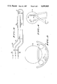
- FIGS. 5 and 6 illustrate in cross-section and perspective views, respectively, a removable feedthrough plate 24 in accordance with the invention.
- the feedthrough plate which can be fabricated from aluminum, stainless steel, or like material, includes a flange 98 which is securely bolted to end cap 20.
- O-ring 99 provides a seal between the feedthrough plate and the end cap.
- the end cap itself is sealed to the end of the reaction tube. The seal to the end of the reaction tube is difficult to make and, accordingly, if possible, that seal is never broken. Instead, all changes to the reactor plumbing are made by removing the feedthrough plate and not by disturbing the end cap.
- Holes 100 are drilled and tapped through the feedthrough plate to accommodate appropriate couplings 102.
- Flexible tube such as 50 and 54 connect to the exterior couplings with a compression fitting.
- the outside couplings and flexible tubes are fabricated from stainless steel or other materials suitable for the handling of corrosive materials.
- the feedthrough plate is unfastened and withdrawn from end cap 20.
- the U-shaped and other injectors are positioned within the reaction chamber so that ends 84,86 and the end of injector 44 protrudes out the hole in the end cap. Connections are made to the ends of the injectors using compression nuts 104 and O-rings 106.
- the assembly of feedthrough plate and injectors is then positioned with the feedthrough plate seated against the end cap and the two bolted together.
- the injectors can be changed, cleaned, or replaced without disturbing the critical seal between the end cap and the reaction tube. None of the fittings are disturbed by the loading or unloading of deposition surfaces into the reaction chamber since those operations are carried out through the opposite end of the tube.
- each refractory metallic film requires specific flow rates, temperatures, pressures, and residence times for optimum deposition rates and uniformity.
- the following nonlimiting examples serve to further illustrate practice of the invention and to demonstrate the optimization of some of these process variables.
- a 170 mm inside diameter, standard, continuously heated diffusion furnace was prepared for the low pressure chemical vapor deposition of a 260 nm: thick film of TiB 2 onto 75 mm and 100 mm silicon wafers during the processing of those wafers in the fabrication of semiconductor discrete devices and integrated circuits.
- a 116 mm outside diameter quartz tube having a length of 2 meters and equipped with opaque quartz rings about 160 mm from each end of the tube was positioned in the furnace and was fitted with O-ring sealed aluminum end caps at each end.
- a quartz sleeve having an outside diameter of 150 mm and having a length of 1.6 meters was centered in the 160 mm tube as a protective liner.
- the end cap at the exhaust end of the tube was provided with a removable feedthrough plate having standard compression fittings facing out and O-ring sealed fittings facing into the furnace.
- a source of TiCl 4 was coupled to the feedthrough plate with 1/4 inch inside diameter stainless steel tubing.
- the TiCl 4 source was coupled through the feedthrough plate to a U-shaped injector as described above.
- the injector was fabricated from 9 mm quartz tubing with 12 injector holes spaced 1 inch apart and having a diameter of 0.050 inches. These holes were drilled through one wall of the inlet arm of the U-shaped injector tube.
- the output end of the U-shaped injector tube was coupled through the feedthrough plate and flexible stainless steel lines to a vacuum pump.
- the vacuum train used a 50 mm exhaust line to connect the reactor to the pump with a 5 mm valve for soft pumping in parallel with a 55 mm valve for hard pumping.
- the vacuum pump was a standard mechanical vacuum pump.
- the LPCVD reactor described in Example 1 was modified for the deposition of a 50 nm film of TiN.
- An NH 3 source was connected to the removable feedthrough plate through a mass flow controller and flexible stainless steel connector. Internal to the reaction chamber, an NH 3 conection was made to a single straight tube injector which contained twelve holes, spaced one inch apart, and each having a diameter of 0.050 inches.
- a hydrogen source was connected to the front (upstream) end cap of the reactor. Semiconductor wafers were loaded into the reactor and the reactor was evacuated as before and brought to the reaction temperature. The pressure during deposition was about 27 Pa.
- a TiN film deposition occured as summarized in the following tables.
- WSi 2 films having a thickness of 400 nm were prepared in the same reactor by replacing the TiCl 4 source with WF 6 and the B 2 H 6 source with SiH 4 .
- the quartz liner and U-shaped injector were replaced to minimize cross-contamination of the WSi 2 films.
- Films of WSi 2 were deposited on semiconductor wafers which were loaded into the upstream end of the reaction chamber. The chamber was evacuated and brought to deposition temperature as above. Results of the deposition are summarized in the table below.
Abstract
Description
WF.sub.6 +2SiH.sub.4 →WSi.sub.2 +6HF +H.sub.2.
TiCl.sub.4 +B.sub.2 H.sub.6 →TiB.sub.2 +4HCl+H.sub.2.
WF.sub.6 +2SiH.sub.4 →WSi.sub.2 +6HF+H.sub.2
WSi.sub.2 +10HF →WF.sub.6 +2H.sub.2 SiF.sub.2 +3H.sub.2.
              TABLE IA
______________________________________
Summary of Parameters For TiB.sub.2 Deposition
Temp. Time     Flow Rates (SCCM)
                                Deposition
(°C.)
      (Min)    TiCl.sub.4
                       B.sub.2 H.sub.6 /H.sub.2
                               Ar   Rate (nm/min)
______________________________________
Run 1.
      30       45      25/475  100  10.0
650
Run 2.
      30       45      25/475  100  8.70
600
______________________________________
              TABLE IB
______________________________________
Physical Properties of TiB.sub.2 Film Deposited at 600° C.
______________________________________
Film Thickness      260 nm
Morphological Appearance
                    Silver Mirror
Boron To Titanium Ratio
                    2.0 To 1
Sheet Resistivity   6.4 Ohms Per Square
Film Uniformity (X-Wafer)
                    ±2.0%
Film Uniformity (X-Boat)
                    ±7.0%
______________________________________
              TABLE IIA
______________________________________
Summary of Parameters for TiN Deposition
Temp. Time    Flow Rates (SCCM)
                            Deposition
                                     Anneal
(°C.)
      (min)   TiCl.sub.4
                      NH.sub.3
                           H.sub.2
                                Rate (m/min)
                                         Temp (°C.)
______________________________________
Run 1.
      30      45      100  100  1.67     900
700
Run 2.
      30      45      100  100  1.83     900
800
______________________________________
              TABLE IIB
______________________________________
Physical Properties of TiN Film Deposited at 700°  C.
______________________________________
Film Thickness     50.0 nm
Morphological Appearance
                   Yellow Gold
Nitrogen To Titanium Ratio
                   1 To 1
Sheet Resistivity  17 Ohms Per Square
Sheet Resistance   85 Micro Ohm Centimeter
Film Uniformity (X-Wafer)
                   ±3.8%
Film Uniformity (X-Boat)
                   ±8.6%
______________________________________
              TABLE IIIA
______________________________________
Summary Of Parameters For WSi.sub.2 Deposition
               Flow Rates
Temp. Time      (SCCM)    Deposition
                                    Anneal
(°C.)
      (min)    WF.sub.6
                      SH.sub.4
                            Rate (nm/min)
                                      Temp (°C.)
______________________________________
Run 1.
      10       25     200   31        650
450
Run 2.
      10       15     200   20        650
450
______________________________________
              TABLE IIIB
______________________________________
Physical Properties of WSi.sub.2 Films Deposited at 450° C.
______________________________________
Film Thickness     310 nm
Morphological Appearance
                   Metallic Silver Grey
Silicon to Tungsten Ratio
                   2.3 To 1
Sheet Resistivity  1.48 Ohms Per Square
Sheet Resistance   46 Micro Ohm Centimeter
Film Uniformity (X-Wafer)
                   ±4.3%
Film Uniformity (X-Boat)
                   ±9%
______________________________________
Claims (25)
Priority Applications (1)
| Application Number | Priority Date | Filing Date | Title |
|---|---|---|---|
| US06/881,988 US4699805A (en) | 1986-07-03 | 1986-07-03 | Process and apparatus for the low pressure chemical vapor deposition of thin films |
Applications Claiming Priority (1)
| Application Number | Priority Date | Filing Date | Title |
|---|---|---|---|
| US06/881,988 US4699805A (en) | 1986-07-03 | 1986-07-03 | Process and apparatus for the low pressure chemical vapor deposition of thin films |
Publications (1)
| Publication Number | Publication Date |
|---|---|
| US4699805A true US4699805A (en) | 1987-10-13 |
Family
ID=25379654
Family Applications (1)
| Application Number | Title | Priority Date | Filing Date |
|---|---|---|---|
| US06/881,988 Expired - Lifetime US4699805A (en) | 1986-07-03 | 1986-07-03 | Process and apparatus for the low pressure chemical vapor deposition of thin films |
Country Status (1)
| Country | Link |
|---|---|
| US (1) | US4699805A (en) |
Cited By (60)
| Publication number | Priority date | Publication date | Assignee | Title |
|---|---|---|---|---|
| US4911638A (en) * | 1989-05-18 | 1990-03-27 | Direction Incorporated | Controlled diffusion environment capsule and system |
| US5029554A (en) * | 1988-03-31 | 1991-07-09 | Kabushiki Kaisha Toshiba | Semiconductor manufacturing apparatus including a temperature control mechanism |
| US5065698A (en) * | 1988-04-11 | 1991-11-19 | Canon Kabushiki Kaisha | Film forming apparatus capable of preventing adhesion of film deposits |
| US5116784A (en) * | 1990-11-30 | 1992-05-26 | Tokyo Electron Limited | Method of forming semiconductor film |
| US5137047A (en) * | 1990-08-24 | 1992-08-11 | Mark George | Delivery of reactive gas from gas pad to process tool |
| US5178534A (en) * | 1989-05-18 | 1993-01-12 | Bayne Christopher J | Controlled diffusion environment capsule and system |
| US5372649A (en) * | 1992-04-06 | 1994-12-13 | Sony Electronics, Inc. | Apparatus for weighting a diffusion furnace cantilever |
| US5427824A (en) * | 1986-09-09 | 1995-06-27 | Semiconductor Energy Laboratory Co., Ltd. | CVD apparatus |
| US5496410A (en) * | 1992-03-10 | 1996-03-05 | Hitachi, Ltd. | Plasma processing apparatus and method of processing substrates by using same apparatus |
| US5571333A (en) * | 1994-06-02 | 1996-11-05 | Shin-Etsu Handotai Co. Ltd. | Heat treatment furnace with an exhaust baffle |
| US5650013A (en) * | 1984-11-26 | 1997-07-22 | Semiconductor Energy Laboratory Co., Ltd. | Layer member forming method |
| US5653808A (en) * | 1996-08-07 | 1997-08-05 | Macleish; Joseph H. | Gas injection system for CVD reactors |
| US5782980A (en) * | 1996-05-14 | 1998-07-21 | Advanced Micro Devices, Inc. | Low pressure chemical vapor deposition apparatus including a process gas heating subsystem |
| US5916369A (en) * | 1995-06-07 | 1999-06-29 | Applied Materials, Inc. | Gas inlets for wafer processing chamber |
| USRE36328E (en) * | 1988-03-31 | 1999-10-05 | Kabushiki Kaisha Toshiba | Semiconductor manufacturing apparatus including temperature control mechanism |
| US5961725A (en) * | 1997-10-21 | 1999-10-05 | Taiwan Semiconductor Manufacturing Company, Ltd. | Conical baffle for semiconductor furnaces |
| US5972078A (en) * | 1997-07-31 | 1999-10-26 | Fsi International, Inc. | Exhaust rinse manifold for use with a coating apparatus |
| US6013338A (en) * | 1986-09-09 | 2000-01-11 | Semiconductor Energy Laboratory Co., Ltd. | CVD apparatus |
| US6056823A (en) * | 1997-09-11 | 2000-05-02 | Applied Materials, Inc. | Temperature controlled gas feedthrough |
| US6099904A (en) * | 1997-12-02 | 2000-08-08 | Applied Materials, Inc. | Low resistivity W using B2 H6 nucleation step |
| US6156382A (en) * | 1997-05-16 | 2000-12-05 | Applied Materials, Inc. | Chemical vapor deposition process for depositing tungsten |
| US6194030B1 (en) | 1999-03-18 | 2001-02-27 | International Business Machines Corporation | Chemical vapor deposition velocity control apparatus |
| US6197373B1 (en) * | 1998-06-03 | 2001-03-06 | Seh America, Inc. | Gas injection methods for a LPCVD furnace |
| US6204197B1 (en) | 1984-02-15 | 2001-03-20 | Semiconductor Energy Laboratory Co., Ltd. | Semiconductor device, manufacturing method, and system |
| US6230650B1 (en) | 1985-10-14 | 2001-05-15 | Semiconductor Energy Laboratory Co., Ltd. | Microwave enhanced CVD system under magnetic field |
| US6383300B1 (en) * | 1998-11-27 | 2002-05-07 | Tokyo Electron Ltd. | Heat treatment apparatus and cleaning method of the same |
| US6399499B1 (en) * | 1999-09-14 | 2002-06-04 | Jeong Gey Lee | Method for fabricating an electrode of a plasma chamber |
| US6500734B2 (en) | 1993-07-30 | 2002-12-31 | Applied Materials, Inc. | Gas inlets for wafer processing chamber |
| US6536460B1 (en) * | 1997-03-21 | 2003-03-25 | Advanced Micro Devices, Inc. | Process line purge system and method |
| US6576062B2 (en) * | 2000-01-06 | 2003-06-10 | Tokyo Electron Limited | Film forming apparatus and film forming method |
| US6673722B1 (en) | 1985-10-14 | 2004-01-06 | Semiconductor Energy Laboratory Co., Ltd. | Microwave enhanced CVD system under magnetic field |
| US6784033B1 (en) | 1984-02-15 | 2004-08-31 | Semiconductor Energy Laboratory Co., Ltd. | Method for the manufacture of an insulated gate field effect semiconductor device |
| US6786997B1 (en) | 1984-11-26 | 2004-09-07 | Semiconductor Energy Laboratory Co., Ltd. | Plasma processing apparatus |
| US6872636B2 (en) * | 2001-03-21 | 2005-03-29 | Hitachi Kokusai Electric Inc. | Method for fabricating a semiconductor device |
| US20050250348A1 (en) * | 2004-05-06 | 2005-11-10 | Applied Materials, Inc. | In-situ oxide capping after CVD low k deposition |
| US20060011135A1 (en) * | 2001-07-06 | 2006-01-19 | Dmitriev Vladimir A | HVPE apparatus for simultaneously producing multiple wafers during a single epitaxial growth run |
| US20060048706A1 (en) * | 2002-09-09 | 2006-03-09 | Electronics And Telecommunications Research I Institute | Apparatus for manufacturing semiconductor device and method for manufacturing semiconductor device by using the same |
| US20060084201A1 (en) * | 2004-10-15 | 2006-04-20 | Albert Hasper | Parts for deposition reactors |
| US20060105107A1 (en) * | 2004-10-15 | 2006-05-18 | Lindeboom Bartholomeus H L | Reactor design for reduced particulate generation |
| US20060196418A1 (en) * | 2005-03-04 | 2006-09-07 | Picosun Oy | Apparatuses and methods for deposition of material on surfaces |
| US20060258174A1 (en) * | 2003-08-15 | 2006-11-16 | Hitachi Kokusai Electric Inc. | Substrate treatment apparatus and method of manufacturing semiconductor device |
| US20060276054A1 (en) * | 2005-06-03 | 2006-12-07 | Applied Materials, Inc. | In situ oxide cap layer development |
| US20070128866A1 (en) * | 2003-08-19 | 2007-06-07 | Sang-Woo Lee | Apparatus for fabricating tungsten contacts with tungsten nitride barrier layers in semiconductor devices |
| US20070141851A1 (en) * | 2005-12-16 | 2007-06-21 | Selen Louis J | System and method of reducing particle contamination of semiconductor substrates |
| US20080127894A1 (en) * | 2001-10-30 | 2008-06-05 | Joseph John Sumakeris | Housing assembly for an induction heating device including liner or susceptor coating |
| US20080173238A1 (en) * | 2006-12-12 | 2008-07-24 | Hitachi Kokusai Electric Inc. | Substrate processing apparatus, method of manufacturing semiconductor device, and reaction vessel |
| US20090223448A1 (en) * | 2008-01-31 | 2009-09-10 | Hitachi Kokusai Electric Inc. | Substrate processing apparatus and method for manufacturing semiconductor device |
| US7629256B2 (en) | 2007-05-14 | 2009-12-08 | Asm International N.V. | In situ silicon and titanium nitride deposition |
| US7691757B2 (en) | 2006-06-22 | 2010-04-06 | Asm International N.V. | Deposition of complex nitride films |
| US20100132614A1 (en) * | 2008-12-01 | 2010-06-03 | Tokyo Electron Limited | Film deposition apparatus |
| US20100133325A1 (en) * | 2008-12-01 | 2010-06-03 | Xerox Corporation | Unified metal alloying in a diffusion furnace |
| US7732350B2 (en) | 2004-09-22 | 2010-06-08 | Asm International N.V. | Chemical vapor deposition of TiN films in a batch reactor |
| US20100147924A1 (en) * | 2008-12-12 | 2010-06-17 | Xerox Corporation | Jet stack brazing in a diffusion furnace |
| US7833906B2 (en) | 2008-12-11 | 2010-11-16 | Asm International N.V. | Titanium silicon nitride deposition |
| US20120264072A1 (en) * | 2011-02-03 | 2012-10-18 | Stion Corporation | Method and apparatus for performing reactive thermal treatment of thin film pv material |
| US20150360242A1 (en) * | 2014-06-11 | 2015-12-17 | Veeco Ald Inc. | Linear Deposition Apparatus with Modular Assembly |
| US20170029945A1 (en) * | 2015-07-29 | 2017-02-02 | Hitachi Kokusai Electric Inc. | Substrate processing apparatus, method of manufacturing semiconductor device, and recording medium |
| KR20180057532A (en) * | 2016-11-21 | 2018-05-30 | 도쿄엘렉트론가부시키가이샤 | Substrate processing apparatus, injector, and substrate processing method |
| CN111902565A (en) * | 2018-04-03 | 2020-11-06 | 全南大学校产学协力团 | Deposition device capable of coating powder particles and coating method of powder particles |
| US20210292905A1 (en) * | 2020-03-18 | 2021-09-23 | Tokyo Electron Limited | Substrate processing apparatus and cleaning method |
Citations (2)
| Publication number | Priority date | Publication date | Assignee | Title |
|---|---|---|---|---|
| US4392299A (en) * | 1981-01-08 | 1983-07-12 | Rca Corporation | Method of manufacturing low resistance gates and interconnections |
| US4619840A (en) * | 1983-05-23 | 1986-10-28 | Thermco Systems, Inc. | Process and apparatus for low pressure chemical vapor deposition of refractory metal |
-
1986
- 1986-07-03 US US06/881,988 patent/US4699805A/en not_active Expired - Lifetime
Patent Citations (2)
| Publication number | Priority date | Publication date | Assignee | Title |
|---|---|---|---|---|
| US4392299A (en) * | 1981-01-08 | 1983-07-12 | Rca Corporation | Method of manufacturing low resistance gates and interconnections |
| US4619840A (en) * | 1983-05-23 | 1986-10-28 | Thermco Systems, Inc. | Process and apparatus for low pressure chemical vapor deposition of refractory metal |
Non-Patent Citations (4)
| Title |
|---|
| C. E. Morosanu and V. Soltuz, "Thin Film Preparation by Plasma and Low Pressure CVD in a Horizontal Reactor", Vacuum, vol. 31, No. 7, pp. 309-313, 1981. |
| C. E. Morosanu and V. Soltuz, Thin Film Preparation by Plasma and Low Pressure CVD in a Horizontal Reactor , Vacuum, vol. 31, No. 7, pp. 309 313, 1981. * |
| M. J. Cooke, "A Review of LPCVD Metallization for Semiconductor Devices", Vacuum, vol. 35, No. 2, pp. 67-73, 1985. |
| M. J. Cooke, A Review of LPCVD Metallization for Semiconductor Devices , Vacuum, vol. 35, No. 2, pp. 67 73, 1985. * |
Cited By (101)
| Publication number | Priority date | Publication date | Assignee | Title |
|---|---|---|---|---|
| US6784033B1 (en) | 1984-02-15 | 2004-08-31 | Semiconductor Energy Laboratory Co., Ltd. | Method for the manufacture of an insulated gate field effect semiconductor device |
| US6204197B1 (en) | 1984-02-15 | 2001-03-20 | Semiconductor Energy Laboratory Co., Ltd. | Semiconductor device, manufacturing method, and system |
| US5650013A (en) * | 1984-11-26 | 1997-07-22 | Semiconductor Energy Laboratory Co., Ltd. | Layer member forming method |
| US6984595B1 (en) | 1984-11-26 | 2006-01-10 | Semiconductor Energy Laboratory Co., Ltd. | Layer member forming method |
| US6786997B1 (en) | 1984-11-26 | 2004-09-07 | Semiconductor Energy Laboratory Co., Ltd. | Plasma processing apparatus |
| US5904567A (en) * | 1984-11-26 | 1999-05-18 | Semiconductor Energy Laboratory Co., Ltd. | Layer member forming method |
| US6673722B1 (en) | 1985-10-14 | 2004-01-06 | Semiconductor Energy Laboratory Co., Ltd. | Microwave enhanced CVD system under magnetic field |
| US6230650B1 (en) | 1985-10-14 | 2001-05-15 | Semiconductor Energy Laboratory Co., Ltd. | Microwave enhanced CVD system under magnetic field |
| US5629245A (en) * | 1986-09-09 | 1997-05-13 | Semiconductor Energy Laboratory Co., Ltd. | Method for forming a multi-layer planarization structure |
| US5427824A (en) * | 1986-09-09 | 1995-06-27 | Semiconductor Energy Laboratory Co., Ltd. | CVD apparatus |
| US5855970A (en) * | 1986-09-09 | 1999-01-05 | Semiconductor Energy Laboratory Co., Ltd. | Method of forming a film on a substrate |
| US6013338A (en) * | 1986-09-09 | 2000-01-11 | Semiconductor Energy Laboratory Co., Ltd. | CVD apparatus |
| US5029554A (en) * | 1988-03-31 | 1991-07-09 | Kabushiki Kaisha Toshiba | Semiconductor manufacturing apparatus including a temperature control mechanism |
| USRE36328E (en) * | 1988-03-31 | 1999-10-05 | Kabushiki Kaisha Toshiba | Semiconductor manufacturing apparatus including temperature control mechanism |
| US5065698A (en) * | 1988-04-11 | 1991-11-19 | Canon Kabushiki Kaisha | Film forming apparatus capable of preventing adhesion of film deposits |
| US5112185A (en) * | 1988-04-14 | 1992-05-12 | Canon Kabushiki Kaisha | Method for replacing a deposit shield in an evacuated film forming chamber |
| US4911638A (en) * | 1989-05-18 | 1990-03-27 | Direction Incorporated | Controlled diffusion environment capsule and system |
| US5178534A (en) * | 1989-05-18 | 1993-01-12 | Bayne Christopher J | Controlled diffusion environment capsule and system |
| EP0473040B1 (en) * | 1990-08-24 | 1995-10-18 | Air Products And Chemicals, Inc. | System for delivery of reactive gases from a source of supply to a tool |
| US5137047A (en) * | 1990-08-24 | 1992-08-11 | Mark George | Delivery of reactive gas from gas pad to process tool |
| US5116784A (en) * | 1990-11-30 | 1992-05-26 | Tokyo Electron Limited | Method of forming semiconductor film |
| US5496410A (en) * | 1992-03-10 | 1996-03-05 | Hitachi, Ltd. | Plasma processing apparatus and method of processing substrates by using same apparatus |
| US5372649A (en) * | 1992-04-06 | 1994-12-13 | Sony Electronics, Inc. | Apparatus for weighting a diffusion furnace cantilever |
| US6500734B2 (en) | 1993-07-30 | 2002-12-31 | Applied Materials, Inc. | Gas inlets for wafer processing chamber |
| US5571333A (en) * | 1994-06-02 | 1996-11-05 | Shin-Etsu Handotai Co. Ltd. | Heat treatment furnace with an exhaust baffle |
| US5916369A (en) * | 1995-06-07 | 1999-06-29 | Applied Materials, Inc. | Gas inlets for wafer processing chamber |
| US5782980A (en) * | 1996-05-14 | 1998-07-21 | Advanced Micro Devices, Inc. | Low pressure chemical vapor deposition apparatus including a process gas heating subsystem |
| US6113984A (en) * | 1996-08-07 | 2000-09-05 | Concept Systems Design, Inc. | Gas injection system for CVD reactors |
| US5653808A (en) * | 1996-08-07 | 1997-08-05 | Macleish; Joseph H. | Gas injection system for CVD reactors |
| US6536460B1 (en) * | 1997-03-21 | 2003-03-25 | Advanced Micro Devices, Inc. | Process line purge system and method |
| US6156382A (en) * | 1997-05-16 | 2000-12-05 | Applied Materials, Inc. | Chemical vapor deposition process for depositing tungsten |
| US5972078A (en) * | 1997-07-31 | 1999-10-26 | Fsi International, Inc. | Exhaust rinse manifold for use with a coating apparatus |
| US6056823A (en) * | 1997-09-11 | 2000-05-02 | Applied Materials, Inc. | Temperature controlled gas feedthrough |
| US6258170B1 (en) * | 1997-09-11 | 2001-07-10 | Applied Materials, Inc. | Vaporization and deposition apparatus |
| US5961725A (en) * | 1997-10-21 | 1999-10-05 | Taiwan Semiconductor Manufacturing Company, Ltd. | Conical baffle for semiconductor furnaces |
| US6206967B1 (en) | 1997-12-02 | 2001-03-27 | Applied Materials, Inc. | Low resistivity W using B2H6 nucleation step |
| US6099904A (en) * | 1997-12-02 | 2000-08-08 | Applied Materials, Inc. | Low resistivity W using B2 H6 nucleation step |
| US6197373B1 (en) * | 1998-06-03 | 2001-03-06 | Seh America, Inc. | Gas injection methods for a LPCVD furnace |
| US6383300B1 (en) * | 1998-11-27 | 2002-05-07 | Tokyo Electron Ltd. | Heat treatment apparatus and cleaning method of the same |
| US6194030B1 (en) | 1999-03-18 | 2001-02-27 | International Business Machines Corporation | Chemical vapor deposition velocity control apparatus |
| US6399499B1 (en) * | 1999-09-14 | 2002-06-04 | Jeong Gey Lee | Method for fabricating an electrode of a plasma chamber |
| US6576062B2 (en) * | 2000-01-06 | 2003-06-10 | Tokyo Electron Limited | Film forming apparatus and film forming method |
| US6872636B2 (en) * | 2001-03-21 | 2005-03-29 | Hitachi Kokusai Electric Inc. | Method for fabricating a semiconductor device |
| US20060011135A1 (en) * | 2001-07-06 | 2006-01-19 | Dmitriev Vladimir A | HVPE apparatus for simultaneously producing multiple wafers during a single epitaxial growth run |
| US9155131B2 (en) | 2001-10-30 | 2015-10-06 | Cree, Inc. | Methods for controllably induction heating an article |
| US7390367B1 (en) * | 2001-10-30 | 2008-06-24 | Cree, Inc. | Housing assembly for an induction heating device including liner or susceptor coating |
| US20090136686A1 (en) * | 2001-10-30 | 2009-05-28 | Cree, Inc. | Methods for Controllably Induction Heating an Article |
| US20080127894A1 (en) * | 2001-10-30 | 2008-06-05 | Joseph John Sumakeris | Housing assembly for an induction heating device including liner or susceptor coating |
| DE10297788B4 (en) * | 2002-09-09 | 2008-06-26 | Electronics And Telecommunications Research Institute | Deposition apparatus for manufacturing semiconductor device, e.g. Schottky barrier metal oxide semiconductor field effect transistor, comprises first and second chambers, pumping portions, gas injecting portions, and connecting portion |
| US20060048706A1 (en) * | 2002-09-09 | 2006-03-09 | Electronics And Telecommunications Research I Institute | Apparatus for manufacturing semiconductor device and method for manufacturing semiconductor device by using the same |
| US8598047B2 (en) | 2003-08-15 | 2013-12-03 | Hitachi Kokusai Electric Inc. | Substrate processing apparatus and producing method of semiconductor device |
| US20060258174A1 (en) * | 2003-08-15 | 2006-11-16 | Hitachi Kokusai Electric Inc. | Substrate treatment apparatus and method of manufacturing semiconductor device |
| US20090186467A1 (en) * | 2003-08-15 | 2009-07-23 | Masanori Sakai | Substrate Processing Apparatus and Producing Method of Semiconductor Device |
| US20070128866A1 (en) * | 2003-08-19 | 2007-06-07 | Sang-Woo Lee | Apparatus for fabricating tungsten contacts with tungsten nitride barrier layers in semiconductor devices |
| US7112541B2 (en) | 2004-05-06 | 2006-09-26 | Applied Materials, Inc. | In-situ oxide capping after CVD low k deposition |
| US20050250348A1 (en) * | 2004-05-06 | 2005-11-10 | Applied Materials, Inc. | In-situ oxide capping after CVD low k deposition |
| US7966969B2 (en) | 2004-09-22 | 2011-06-28 | Asm International N.V. | Deposition of TiN films in a batch reactor |
| US7732350B2 (en) | 2004-09-22 | 2010-06-08 | Asm International N.V. | Chemical vapor deposition of TiN films in a batch reactor |
| US7674726B2 (en) | 2004-10-15 | 2010-03-09 | Asm International N.V. | Parts for deposition reactors |
| US20060084201A1 (en) * | 2004-10-15 | 2006-04-20 | Albert Hasper | Parts for deposition reactors |
| US7427571B2 (en) | 2004-10-15 | 2008-09-23 | Asm International, N.V. | Reactor design for reduced particulate generation |
| US20060105107A1 (en) * | 2004-10-15 | 2006-05-18 | Lindeboom Bartholomeus H L | Reactor design for reduced particulate generation |
| US20060196418A1 (en) * | 2005-03-04 | 2006-09-07 | Picosun Oy | Apparatuses and methods for deposition of material on surfaces |
| US8211235B2 (en) * | 2005-03-04 | 2012-07-03 | Picosun Oy | Apparatuses and methods for deposition of material on surfaces |
| US7273823B2 (en) | 2005-06-03 | 2007-09-25 | Applied Materials, Inc. | Situ oxide cap layer development |
| US20060276054A1 (en) * | 2005-06-03 | 2006-12-07 | Applied Materials, Inc. | In situ oxide cap layer development |
| US7553516B2 (en) | 2005-12-16 | 2009-06-30 | Asm International N.V. | System and method of reducing particle contamination of semiconductor substrates |
| US20070141851A1 (en) * | 2005-12-16 | 2007-06-21 | Selen Louis J | System and method of reducing particle contamination of semiconductor substrates |
| US7691757B2 (en) | 2006-06-22 | 2010-04-06 | Asm International N.V. | Deposition of complex nitride films |
| US8420167B2 (en) * | 2006-12-12 | 2013-04-16 | Hitachi Kokusai Electric Inc. | Method of manufacturing a semiconductor device |
| US20090191718A1 (en) * | 2006-12-12 | 2009-07-30 | Hitachi Kokusai Electric Inc. | Substrate processing apparatus, method of manufacturing semiconductor device, and reaction vessel |
| US20080173238A1 (en) * | 2006-12-12 | 2008-07-24 | Hitachi Kokusai Electric Inc. | Substrate processing apparatus, method of manufacturing semiconductor device, and reaction vessel |
| US7629256B2 (en) | 2007-05-14 | 2009-12-08 | Asm International N.V. | In situ silicon and titanium nitride deposition |
| US20120122318A1 (en) * | 2008-01-31 | 2012-05-17 | Hitachi Kokusai Electric Inc. | Substrate processing apparatus and method for manufacturing semiconductor device |
| US20090223448A1 (en) * | 2008-01-31 | 2009-09-10 | Hitachi Kokusai Electric Inc. | Substrate processing apparatus and method for manufacturing semiconductor device |
| US8461062B2 (en) * | 2008-01-31 | 2013-06-11 | Hitachi Kokusai Electric Inc. | Substrate processing apparatus and method for manufacturing semiconductor device |
| US8828141B2 (en) * | 2008-01-31 | 2014-09-09 | Hitachi Kokusai Electric Inc. | Substrate processing apparatus and method for manufacturing semiconductor device |
| US9297072B2 (en) * | 2008-12-01 | 2016-03-29 | Tokyo Electron Limited | Film deposition apparatus |
| US20100133325A1 (en) * | 2008-12-01 | 2010-06-03 | Xerox Corporation | Unified metal alloying in a diffusion furnace |
| US20100132614A1 (en) * | 2008-12-01 | 2010-06-03 | Tokyo Electron Limited | Film deposition apparatus |
| US7833906B2 (en) | 2008-12-11 | 2010-11-16 | Asm International N.V. | Titanium silicon nitride deposition |
| US7980447B2 (en) * | 2008-12-12 | 2011-07-19 | Xerox Corporation | Jet stack brazing in a diffusion furnace |
| US20110226839A1 (en) * | 2008-12-12 | 2011-09-22 | Xerox Corporation | Jet stack brazing in a diffusion furnace |
| US8152045B2 (en) | 2008-12-12 | 2012-04-10 | Xerox Corporation | Jet stack brazing in a diffusion furnace |
| US20100147924A1 (en) * | 2008-12-12 | 2010-06-17 | Xerox Corporation | Jet stack brazing in a diffusion furnace |
| US8505803B2 (en) | 2008-12-12 | 2013-08-13 | Xerox Corporation | Jet stack brazing in a diffusion furnace |
| TWI479671B (en) * | 2011-02-03 | 2015-04-01 | Stion Corp | Method and apparatus for performing reactive thermal treatment of thin film pv material |
| CN102820372A (en) * | 2011-02-03 | 2012-12-12 | 思阳公司 | Method and apparatus for performing reactive thermal treatment of thin film pv material |
| US20120264072A1 (en) * | 2011-02-03 | 2012-10-18 | Stion Corporation | Method and apparatus for performing reactive thermal treatment of thin film pv material |
| US20150360242A1 (en) * | 2014-06-11 | 2015-12-17 | Veeco Ald Inc. | Linear Deposition Apparatus with Modular Assembly |
| US20170029945A1 (en) * | 2015-07-29 | 2017-02-02 | Hitachi Kokusai Electric Inc. | Substrate processing apparatus, method of manufacturing semiconductor device, and recording medium |
| JP2017033974A (en) * | 2015-07-29 | 2017-02-09 | 株式会社日立国際電気 | Substrate processing apparatus, manufacturing method of semiconductor device, program, and gas supply pipe |
| US10655218B2 (en) * | 2015-07-29 | 2020-05-19 | Kokusai Electric Corporation | Substrate processing apparatus, method of manufacturing semiconductor device, and recording medium |
| JP2018085393A (en) * | 2016-11-21 | 2018-05-31 | 東京エレクトロン株式会社 | Substrate processing device, injector, and substrate processing method |
| KR20180057532A (en) * | 2016-11-21 | 2018-05-30 | 도쿄엘렉트론가부시키가이샤 | Substrate processing apparatus, injector, and substrate processing method |
| KR102230543B1 (en) | 2016-11-21 | 2021-03-19 | 도쿄엘렉트론가부시키가이샤 | Substrate processing apparatus, injector, and substrate processing method |
| CN111902565A (en) * | 2018-04-03 | 2020-11-06 | 全南大学校产学协力团 | Deposition device capable of coating powder particles and coating method of powder particles |
| EP3778986A4 (en) * | 2018-04-03 | 2021-12-15 | Industry Foundation of Chonnam National University | Deposition apparatus capable of applying powder particles, and method for applying powder particles |
| CN111902565B (en) * | 2018-04-03 | 2022-06-24 | 全南大学校产学协力团 | Deposition device capable of coating powder particles and coating method of powder particles |
| US11434566B2 (en) * | 2018-04-03 | 2022-09-06 | Industry Foundation Of Chonnam National University | Deposition apparatus capable of applying powder particles, and method for applying powder particles |
| US20210292905A1 (en) * | 2020-03-18 | 2021-09-23 | Tokyo Electron Limited | Substrate processing apparatus and cleaning method |
Similar Documents
| Publication | Publication Date | Title |
|---|---|---|
| US4699805A (en) | Process and apparatus for the low pressure chemical vapor deposition of thin films | |
| CN107868944B (en) | Titanium nitride atomic layer deposition device and deposition method thereof | |
| EP0464515B1 (en) | Method of manufacturing silicon nitride film | |
| US4098923A (en) | Pyrolytic deposition of silicon dioxide on semiconductors using a shrouded boat | |
| US7569501B2 (en) | ALD metal oxide deposition process using direct oxidation | |
| TW521101B (en) | Compound gas injection system and methods | |
| KR101390425B1 (en) | Temperature-controlled Purge gate valve for Chemical Vapor Deposition Chamber | |
| US4747368A (en) | Chemical vapor deposition apparatus with manifold enveloped by cooling means | |
| EP0637058B1 (en) | Method of supplying reactant gas to a substrate processing apparatus | |
| US6924223B2 (en) | Method of forming a metal layer using an intermittent precursor gas flow process | |
| US7629256B2 (en) | In situ silicon and titanium nitride deposition | |
| US20070292974A1 (en) | Substrate Processing Method and Substrate Processing Apparatus | |
| US20080038486A1 (en) | Radical Assisted Batch Film Deposition | |
| US20040011504A1 (en) | Method and apparatus for gas temperature control in a semiconductor processing system | |
| US20040255868A1 (en) | Plasma etch resistant coating and process | |
| KR20120028305A (en) | Method and apparatus for growing a thin film onto a substrate | |
| JPH07153707A (en) | Accumulation of silicon nitride | |
| WO2004007795A1 (en) | Film formation method for semiconductor processing | |
| US5264038A (en) | Chemical vapor deposition system | |
| KR900008970B1 (en) | Process vapor growth of phosphosilicate glass coating | |
| US5180692A (en) | Method for the manufacture of boron-containing films by CVD or epitaxial techniques using boron trifluoride | |
| CN112575312B (en) | Film preparation equipment and film preparation method | |
| JP2012069844A (en) | Method of manufacturing semiconductor device and substrate processing apparatus | |
| JPH10154702A (en) | Manufacturing method of semiconductor device | |
| JP7349341B2 (en) | Vapor phase growth apparatus and vapor phase growth method |
Legal Events
| Date | Code | Title | Description |
|---|---|---|---|
| AS | Assignment |
Owner name: MOTOROLA, INC., SCHAUMBURG, ILLINOIS, A CORP. OF D Free format text: ASSIGNMENT OF ASSIGNORS INTEREST.;ASSIGNORS:SEELBACH, CHRISTIAN A.;INGLE, WILLIAM M.;GOETZ, CARL A.;REEL/FRAME:004575/0705 Effective date: 19860630 |
|
| STCF | Information on status: patent grant |
Free format text: PATENTED CASE |
|
| FPAY | Fee payment |
Year of fee payment: 4 |
|
| FEPP | Fee payment procedure |
Free format text: PAYOR NUMBER ASSIGNED (ORIGINAL EVENT CODE: ASPN); ENTITY STATUS OF PATENT OWNER: LARGE ENTITY |
|
| FPAY | Fee payment |
Year of fee payment: 8 |
|
| REMI | Maintenance fee reminder mailed | ||
| FPAY | Fee payment |
Year of fee payment: 12 |
|
| SULP | Surcharge for late payment | ||
| AS | Assignment |
Owner name: FREESCALE SEMICONDUCTOR, INC., TEXAS Free format text: ASSIGNMENT OF ASSIGNORS INTEREST;ASSIGNOR:MOTOROLA, INC.;REEL/FRAME:015698/0657 Effective date: 20040404 Owner name: FREESCALE SEMICONDUCTOR, INC.,TEXAS Free format text: ASSIGNMENT OF ASSIGNORS INTEREST;ASSIGNOR:MOTOROLA, INC.;REEL/FRAME:015698/0657 Effective date: 20040404 |