US4701920A - Built-in self-test system for VLSI circuit chips - Google Patents

Built-in self-test system for VLSI circuit chips Download PDF

Info

Publication number
US4701920A
US4701920A US06/796,598 US79659885A US4701920A US 4701920 A US4701920 A US 4701920A US 79659885 A US79659885 A US 79659885A US 4701920 A US4701920 A US 4701920A
Authority
US
United States
Prior art keywords
test
test data
signal
clock
control
Prior art date
Legal status (The legal status is an assumption and is not a legal conclusion. Google has not performed a legal analysis and makes no representation as to the accuracy of the status listed.)
Expired - Fee Related
Application number
US06/796,598
Inventor
David R. Resnick
Randall E. Bach
Current Assignee (The listed assignees may be inaccurate. Google has not performed a legal analysis and makes no representation or warranty as to the accuracy of the list.)
Control Data Corp
Original Assignee
ETA SYSTEMS Inc
Priority date (The priority date is an assumption and is not a legal conclusion. Google has not performed a legal analysis and makes no representation as to the accuracy of the date listed.)
Filing date
Publication date
Application filed by ETA SYSTEMS Inc filed Critical ETA SYSTEMS Inc
Priority to US06/796,598 priority Critical patent/US4701920A/en
Assigned to ETA SYSTEMS, INC., A CORP OF MINNESOTA reassignment ETA SYSTEMS, INC., A CORP OF MINNESOTA ASSIGNMENT OF ASSIGNORS INTEREST. Assignors: BACH, RANDALL E., RESNICK, DAVID R.
Priority to EP19860907130 priority patent/EP0245463A4/en
Priority to JP61506311A priority patent/JPS63501660A/en
Priority to PCT/US1986/002392 priority patent/WO1987003098A1/en
Priority to CA000522584A priority patent/CA1244965A/en
Application granted granted Critical
Publication of US4701920A publication Critical patent/US4701920A/en
Assigned to CONTROL DATA CORPORATION reassignment CONTROL DATA CORPORATION ASSIGNMENT OF ASSIGNORS INTEREST. Assignors: ETA SYSTEMS
Anticipated expiration legal-status Critical
Expired - Fee Related legal-status Critical Current

Links

Images

Classifications

    • GPHYSICS
    • G06COMPUTING; CALCULATING OR COUNTING
    • G06FELECTRIC DIGITAL DATA PROCESSING
    • G06F11/00Error detection; Error correction; Monitoring
    • G06F11/22Detection or location of defective computer hardware by testing during standby operation or during idle time, e.g. start-up testing
    • G06F11/26Functional testing
    • G06F11/27Built-in tests

Definitions

  • the present invention relates to apparatus for testing VLSI circuit chips.
  • the present invention is an improved built-in self-test system for VLSI circuit chips.
  • VLSI circuit chips manufactured with modern integrated circuit (IC) technologies routinely hold over 10,000 devices (eg. transistors). VLSI circuits with 500,000 devices have been developed. The present trend in integrated circuit design is toward even higher levels of circuit integration, thereby reducing costs and improving circuit reliability. As IC technologies continue to develop, it is expected that circuits with at least 100,000,000 devices will become common.
  • Scan design requires the circuit designer to break complex logic circuits into smaller blocks, and to include artificial pathways into and between the blocks for data transmission. Complex sequential circuitry is thereby temporarily converted to combinational circuitry for testing purposes.
  • Scan design techniques are far from optimal. Scan design does not, in general, permit faults to be isolated to a particular chip or wire net. The inclusion of additional test points and transmission paths required for scan design degrades overall IC performance. Scan design also requires additional clock circuitry and relatively complicated maintenance software.
  • BIST built-in self-test
  • test systems are fabricated on the IC chip to be tested.
  • BIST systems include a pattern or operand generator for producing test operands.
  • Each test operand is applied to the IC logic, and the response thereto analyzed by means of a shift register.
  • the response to thousands, and even millions, of test operands is then compressed into a "signature", which is compared to predetermined signatures for a go/no go indication of the IC's operation.
  • One such BIST system is disclosed in the Van Brunt U.S. Pat. No. 4,357,703.
  • BIST has minimal impact upon main logic functions since it is typically fabricated on the sparsely used peripheral areas of the integrated circuit chip. Since test results are processed by the BIST system, the number of tasks which must be performed by external test equipment is reduced. Specially developed maintenance software is therefore greatly reduced. Dynamic testing at full systme clock rates significantly reduces system test times. BIST systems can also be used for testing integrated circuits at the wafer, chip, and system levels. Since they are independent of specific chip logic functions, BIST test systems can be used on any number of different types of circuit chips. The BIST approach also permits IC chips to be tested after they have been assembled into a computer, even though they are inaccessible to more traditional maintenance techniques. This will be the case, for example, when the IC is immersed in a liquid coolant to increase its performance.
  • BIST test systems have yet to be developed to their full potential.
  • BIST systems like that disclosed in U.S. Pat. No. 4,357,703 require the logic designer to carefully synchronize BIST test system control signals with the IC system clock. Only by accurately tuning these control signals can timing violations be avoided. Unless the logic designer pays careful attention to the logic state of the system clock, data held or stored within shift registers of this system will be lost. Although alternate test data from the main logic function could be outputted from this BIST test system, the logic designer was required to actively block the alternate test data when normal test data was being analyzed. In general, the BIST system disclosed in U.S. Pat. No. 4,357,703 constrained logic design.
  • the present invention is an improved built-in self-test system means adapted for fabrication on an LSI circuit chip which incldues main logic function means for performing digital logic operations.
  • the built-in self-test system is interconnected to the main logic function means for performing dynamic tests of main logic function operations.
  • the improvements reduce design constraints imposed upon logic designers by the built-in self-test system.
  • test data in a serial format is received by test data input means.
  • a clock signal which switches between first and second logic states is received by clock input means.
  • Shift register means are responsive to the test data input means and the clock input means and are comprised of a series of static flip-flops for storing and serially transferring test data. The use of static flip-flops permits data stored within the shift register means to be maintained irrespective of the logic state of the clock signal.
  • the built-in self-test system includes test data input means for receiving test data, test strobe input means for receiving a test strobe signal, test clock enable input means for receiving a test clock enable signal, and system clock input means for receiving a system clock signal.
  • Test strobe latch means are responsive to the test strobe input means and the system clock input means and produce a latched test strobe signal.
  • a control register clock signal is produced as a logical function of the system clock signal, the latched test strobe signal, and the latched test clock enable signal by first logic gate means.
  • Control register means responsive to the test data input means serially transfer test data when clocked by the control register clock signal.
  • test strobe latch means and the test clock enable latch means simplify a logic designer's job in that the test strobe and the test clock enable signals need no longer be accurately synchronized, or tuned, with respect to the system clock signal. Test system design is facilitated, thereby reducing overall chip testing costs.
  • the built-in self-test system includes test data input means for receiving test data, and test data output means from which test data is outputted.
  • Control register means are responsive to the test data input means and produce test system control signals including an alternate test data select signal and a normal test data select signal.
  • Shift register means are responsive to the control register means for serial test data transfer, and responsive to the main logic function means for parallel test data transfer.
  • Test data output control means are responsive to the shift register means, the main logic function means, and the control register means. The test data output control means causes alternate test data, from an internal signal node of the main logic function means, to be supplied to the test data output means when the control register means produces the alternate test data select signal.
  • Test data from the shift register means is supplied to the test data output means by the test data output control means when the control register means produces a normal test data select signal. The logic designer is no longer required to block those data paths which are not selected.
  • FIG. 1 is a block diagram representation of a VLSI circuit chip which includes the BIST test system of the present invention.
  • FIG. 2 is a detailed schematic representation of the control logic and test data transfer logic.
  • FIG. 3 is a detailed schematic representation of the control register.
  • FIG. 4 is a description of the BIST functions controlled by control nodes N0-N23 of the control register.
  • FIG. 5 is a detailed schematic representation of the input register and operand generator.
  • FIG. 6 is a detailed schematic representation of the output register and checksum logic.
  • FIG. 7 is a detailed schematic representation of the test data output control logic.
  • FIG. 8 is a detailed schematic representation of the output buffers.
  • the present invention is built-in self-test system for very large-scale integrated circuit chips.
  • built-in self-test (BIST) system 10 is fabricated on a very large-scale integrated (VLSI) circuit chip 12 which includes main logic function 14.
  • main logic function 14 will typically include tens or even hundreds of thousands of electronic devices such as transistors or FETs, and comprise a major portion of the surface area of integrated circuit chip 12.
  • BIST system 10 can be adapted for use with all types of main logic function 14.
  • main logic function 14 can include gate arrays, memory chips, or other custom integrated circuit chips.
  • BIST system 10 is adapted for use with a 20K CMOS gate array.
  • Integrated circuit chip 12 includes a plurality (238 in one embodiment) of input pins 18 on which input data is received.
  • Main logic function 14 is connected to receive the input data through a plurality of input lines 20. Output data produced by main logic function 14 is outputted from integrated circuit 12 on output pins 22 through output lines 24. As shown, each output line 24 includes sections 24A, 24B, and 24C.
  • integrated circuit chip 12 has 140 output lines 24 and output pins 22.
  • Main logic function 14 can be electrically disconnected, or isolated, from input pins 18 and output pins 22 by means of transmission gates 28 and 30, respectively. Transmission gates 30 interface output line sections 24A and 24B. Transmission gates 28 and 30 are under the direct control of BIST system 10, as will be described subsequently in greater detail.
  • BIST system 10 includes control register 32, test data transfer logic 34, input register and operand generator 36 (hereafter referred to as input register 36), output register and checksum logic 38 (hereafter referred to output register 38), test data output control logic 40, and control logic 42.
  • Control logic 42 is connected to receive a system clock (SYS CLK) signal from SYS CLK input pin 44, a test clock enable (TCE) signal on TCE input pin 46, and a test strobe (TS) signal from TS input pin 48.
  • SYS CLK system clock
  • TCE test clock enable
  • TS test strobe
  • Control register 32 is connected to receive test data, in serial format, through test data input (TDI) pin 50.
  • Control register clock (CLK) and ENABLE control signals are received from control logic 42.
  • test data is serially shifted through control register 32, with function codes included therein being produced as control signals at control nodes N0-N23.
  • control signals from control nodes N0-N23 are distributed throughout integrated circuit 12. The function of control signals at control nodes N0-N23 will be described in subsequent portions of this specification.
  • Input register 36 is connected to receive serial test data from test data transfer logic 34, and an input register clock (CLK) signal from control logic 42.
  • Test data transfer logic 34 under the control of a test data select (TDS) control signal produced by control logic 42, causes test data to be supplied to input register 36 either directly from TDI pin 50, or from control register 32.
  • Input register 36 is also connected for parallel test data transfer with input lines 20 through transmission gates 52.
  • Output register 38 is connected to receive serial test data from input register 36, and an output register clock (CLK) signal from control logic 42. Output register 38 is also connected for parallel, bi-directional test data transfer with output lines 24 through transmission gates 54 and 56. As shown, output register 38 can transfer data through transmission gate 54 to output lines 24 at a point intermediate transmission gates 30 and output buffers 26. Test data from output lines 24 at a point either between transmission gates 30 and output buffers 26, or between output buffers 26 and output pins 22, is received by output register 38 through transmission gates 56.
  • CLK output register clock
  • Test data output control logic 40 controls the transfer of test data from BIST system 10 to test data output (TDO) pin 60 in response to control signals received from control nodes N0 and N1 of control register 32.
  • test data output control logic 40 can supply alternate test data from main logic function 14 (as schematically illustrated by node A), a copy of the SYS CLK signal, or an internal test frequency signal such as that produced by oscillator 62, to TDO pin 60.
  • Control logic 42 and test data transfer logic 34 are schematically illustrated in FIG. 2.
  • Control logic 42 includes buffers 70, 72, and 74, latches 76 and 78, flip-flop 80, and NAND gates 82 and 84.
  • Latches 76 and 78 are preferably positive level triggered D-type latches, both of which have a data or D input terminal, and a clock or C input terminal.
  • Latch 76 has a non-inverting output terminal 86 and an inverting output terminal 88, while latch 78 has a non-inverting output terminal 90.
  • Latches 76 and 78 are common circuit elements, and their operation is well known.
  • the logic state (i.e. a "LOW” or logic 0 logic state, or a “HIGH” or logic 1 state) of data produced by on their non-inverting output terminals 86 and 90 will follow, or have the same logic state as, data received on the D input terminal so long as a signal received at the C input terminal has the logic 1 state.
  • the signal applied to the C input terminal is raised, or switched from the logic 0 state to a logic 1 state, the logic state of data then present at the D input terminal is latched, or fixed, at non-inverting output terminals 86 and 90.
  • Flip-flop 80 is preferrably a positive transition edge triggered D-type flip-flop. As shown in FIG. 2, flip-flop 80 has a data or D input terminal, a clock or C input terminal, and a non-inverting output terminal 92. When the signal received at the C input terminal of flip-flop 80 is raised, or switched from a logic 0 state to a logic 1 state, the logic state of the data signal then present at the D input terminal is strobed, or fixed, onto non-inverting output terminal 92. A logic state of the signal on non-inverting output terminal 92 can change states in this manner only when the signal applied to the C input terminal is raised.
  • NAND gate 82 is a 3-input gate having first, second, and third input terminals 84, 96, and 98, respectively, and output terminal 100.
  • NAND gate 84 is a 2-input gate having first and second input terminals 102 and 104, respectively, and output terminal 106.
  • NAND gates 82 and 84 are common circuit elements which perform a logical NAND operation on signals received at their respective input terminals. Simply put, output terminals 100 and 106 of NAND gates 88 and 84, respectively, will be at logic 1 state unless all input terminals of the respective gates receive a signal having a logic 1 state, in which case output terminals 100 and 106 will be at a logic 0 state.
  • Buffers 70, 72 and 74 have input terminals 67, 69, and 71, respectively, and output terminals 73, 75, and 77, respectively. Buffers 70, 72, and 74 produce output signals having the same logic states as the signals received at their input terminals.
  • the system clock (SYS CLK) signal is applied, through buffer 74, to first input terminals 94 and 102 of NAND gates 82 and 84, respectively, and to the C input terminal of latches 76, 78, and flip-flop 80.
  • the test strobe (TS) signal is applied to the D input terminal of latch 76 through buffer 70.
  • Latch 76 latches the logic state of the TS signal onto its output terminals 86 and 88 when SYS CLK raises from the logic 0 to the logic 1 sate, thereby producing a "latched" TS signal.
  • the latched TS signal from non-inverting output terminal 86 is applied to the D input terminal of flip-flop 80, from which it is strobed to non-inverting output terminal 92 upon a succeeding positive transition of SYS CLK.
  • the latched TS signal is a control signal which is applied to the ENABLE control terminal of control register of 32.
  • the logic state of the control register ENABLE signal will follow that of TS after one cycle of SYS CLK.
  • the test clock enable (TCE) signal is applied to the D input terminal of latch 78 through buffer 72.
  • Latch 78 latches the logic state of the TCE signal when SYS CLK is raised from the logic 0 state to the logic 1 state, thereby producing a "latched" TCE signal on its non-inverting output terminal 90.
  • the latched TCE signal is applied to second input terminal 96 and 104 of NAND gates 82 and 84, respectively.
  • the latched TCE signal is gated with the SYS CLK signal by NAND gate 84.
  • the signal present on output terminal 106 of NAND gate 84 is applied to the clock (CLK) input terminal of input register 36, output register 38, and test data output control logic 40.
  • Third input terminal 98 of NAND gate 82 is connected to receive the latched TS signal from inverting output terminal 88 of latch 76. NAND gate 82 thereby gates the latched TS and TCE signals with the SYS CLK signal. The gated TS and TCE signals are output NAND gate 82 at output terminal 100, and applied to the clock (CLK) terminal of control register 32 as shown.
  • Test data select logic 34 includes inverter 110, first and second transmission gates 112 and 114, respectively, and buffer 116.
  • Transmission gate 112 has an input terminal 117, an output terminal 118, a non-inverting control terminal 120, and inverting control terminal 122.
  • Second transmission gate 114 has an input terminal 124, an output terminal 126, a non-inverting control terminal 128, and an inverting control terminal 130.
  • Inverter 110 has an input terminal 109, and an inverting output terminal 111.
  • Inverter 110 and transmission gates 112 and 114 are common circuit elements, the operation of which are well known. Inverter 110 inverts the logic state of the signal received at its input terminal 109. A signal having a logic 1 state at input terminal 109, for example, would be converted to a signal having a logic 0 state at output terminal 111.
  • Transmission gates 112 and 114 function in an identical manner. The following description of transmission gate 112 therefore applies to transmission gate 114, and other transmission gates yet to be described.
  • Transmission gate 112 functions much like a switch and controls the transmission of signals between its input terminal 117 and output terminal 118 in response to control signals received at its control terminals 120 and 122. Transmission gate 112 is driven to its OFF state thereby electrically disconnecting input terminal 117 from output terminal 118, and prohibiting the flow of data therebetween, when a signal having a logic 1 state is applied to inverting control terminal 122 and a signal having a logic 0 state is applied to non-inverting control terminal 120.
  • transmission gate 112 When a signal having a logic 0 state is applied to inverting control terminal 122, and a signal having a logic 1 state is applied to non-inverting control terminal 120, transmission gate 112 will be in its ON state. In its ON state, input terminal 117 is electrically connected to output terminal 118, and data transfer permitted.
  • the latched TS signal from inverting output terminal 88 of latch 76 is applied to test data transfer logic 34 as a test data select (TDS) signal.
  • Input terminal 109 of inverter 110, inverting control terminal 130 of transmission gate 114, and non-inverting control terminal 120 of transmission gate 112 are all connected to receive the latched TS signal.
  • Output terminal 111 of inverter 110 is connected to non-inverting control terminal 128 of transmission gate 114, and inverting control terminal 122 of transmission gate 112.
  • Input terminal 117 of transmission gate 112 is connected to receive test data from control register 32.
  • Input terminal 124 of transmission gate 114 is connected to receive test data directly from TDI pin 38.
  • Output terminals 118 and 126 of transmission gates 112 and 114, respectively, are both applied to input register 36 through buffer 116.
  • test data transfer logic 34 When the TDS signal (latched test strobe signal) received by test data transfer logic 34 has logic 1 state, transmission gate 112 will be ON, while transmission gate 114 will be OFF. Test data from control register 32 will thereby be propogated to input register 36. When the test data select signal has a logic 0 state, transmission gate 114 will be ON, while transmission gate 112 will be OFF. Test data from test data input pin 38 will thereby be propogated to input register 36, bypassing control register 32.
  • Latches 76, 78, and flip-flop 80 greatly simplify the job of a logic designer designing main logic function 14 and test procedures for BIST system 10.
  • TS and TCE signals need no longer be accurately synchronized, or tuned, with the system clock signal.
  • "runt" pulses, long or short set up paths, and other timing violations which can cause errors in the system operation can be reduced. This improvement is especially significant when it is understood that at the extremely high speeds at which BIST system 10 operates, it was previously virtually impossible for the logic designer to accurately predict and account for all possible timing violations.
  • latches 76, 78, and flip-flop 80 effectively reduce overall chip testing costs.
  • FIG. 3 is a schematic representation of control register 32.
  • control register 32 is a 24 bit (i.e. bits 0-23) shift register and is formed by a series arrangement of static flip-flops 150.
  • Each flip-flop 150 has a data or D input terminal, a clock or C input terminal, and an output terminal 152.
  • Test data from TDI pin 50 is inputted the D input terminal of bit 0 flip-flop 150 through buffer 160.
  • output terminal 152 of each flip-flop 150 is connected to the D input terminal of the succeeding flip-flop 150.
  • Output terminal 152 of bit 23 flip-flop 150 is connected, through buffer 162, to test data transfer logic 34.
  • the C input terminal of each flip-flop 150 is connected to receive the control register clock signal (CLK) produced by control logic 42.
  • CLK control register clock signal
  • Each NAND gate 154 has a first input terminal 158 connected to output terminal 152 of its respective flip-flop 150, and a second input terminal 156 connected to receive the control register ENABLE signal produced by control logic 42.
  • An output of each NAND gate 154 is a control node.
  • Control nodes N0-N23 are associated with bits 0-23, respectively. Control nodes N0-N23 are connected to various circuit elements of BIST system 10, as illustrated in FIG. 1.
  • Buffers 160, 162, and NAND gates 154 are common circuit elements. The operation NAND gates such as 154 has been previously described.
  • Flip-flops 150 of control register 32 are all static flip-flops, and are preferrably negative edge triggered. A logic state of a data signal present at the D input terminal of each flip-flop 150 will be strobed to the respective output terminal 152 upon negative (i.e. logic 1 to logic 0) transitions of the control register clock signal.
  • Test data is serially shifted through bits 0-23 of control register 32 at a rate of 1 bit per cycle of the control register clock signal. After 24 cycles of the control register clock signal, for example, the logic state of the data signal originally present at the D input terminal of bit 0 flip-flop 150 will have been shifted to output terminal 152 of bit 23 flip-flop 150.
  • Control register 32 is "loaded” by serially shifting test data including function codes through flip-flops 150.
  • the function code is representative of a desired operational state of BIST system 10, the and is “enabled” when the control register ENABLE signal is raised from a logic 0 state to a logic 1 state (i.e. when TS is raised).
  • control nodes N0-N23 Once enabled, individual bits of the function code are passed to control nodes N0-N23 through respective NAND gates 154, and used as control signals. Circuit elements controlled by the control signals on nodes N0-N23 are thereby driven to their desired operational state. While TS is at a logic 1 state the control register clock is blocked (i.e. maintained at a logic 0 state) freezing the function code in control register 32. As previously discussed, TDI pin 50 will also be connected directly to input register 36, bypassing control register 32, so that the function code in control register 32 will remain valid while test data is being shifted, if desired.
  • control bits N0-N9 are dedicated to the control of various gating functions required to implement all test modes of BIST system 10.
  • Remaining control nodes N10-N23 are "spare" bits that a logic designer can use to control main logic function 14 and thereby enhance its testability.
  • the functions of bits 0-9 and their respective control nodes N0-N9 are described in FIG. 4. These functions are also illustrated in FIG. 1 by the interconnections of control nodes N0-N9 with the circuit elements of BIST system 10.
  • the states of all control nodes are arranged so that when the control register ENABLE signal is dropped to a logic 0 state, (i.e.
  • Control nodes N0-N23 are all active "LO" (i.e., when the control signal thereon has logic 0 state).
  • the static flip-flops 150 used to implement control register 32 permit data to be maintained, or stored, at output terminals 152 irrespective of the logic state of the control register clock signal (i.e. logic states of TS, TCE, and SYS CLK).
  • the logic state of the data signal at output terminal 152 of flip-flops 150 will remain constant, and thereby be stored, if the control register clock is stopped at either a logic 1 or a logic 0 level.
  • TS and TCE need no longer be carefully tuned with respect to the system clock signal.
  • the logic designers attention need no longer be focused on SYS CLK. Design constraints imposed upon logic designers are thereby removed permitting greater flexibility in designing main logic function 14 for testibility.
  • Input register and operand generator 36 (input register 36) is schematically represented in FIG. 5.
  • input register 36 is a 238-bit (i.e. bits 0-237) shift register formed by a series arrangement of static flip-flops 170.
  • Each flip-flop 170 has a data or D input terminal, a clock or C input terminal, and an output terminal 180.
  • Test data from test data transfer logic 34 is inputted to the D input terminal of bit 0 flip-flop 170.
  • Output terminal 180 of bit 0-237 flip-flops 170 is connected to the D input terminal of the following flip-flop 170.
  • Output terminal 180 of bit 237 flip-flop 170 is connected to output register 38.
  • each flip-flop 170 is connected to receive the input register clock (CLK) signal from control logic 42.
  • CLK input register clock
  • Each flip-flop 170 is associated with one of input lines 20, and has its D input terminal operatively connected to the respective input line 20 through transmission gates 52 as illustrated.
  • Input register 36 also includes operand generator logic 172, and serial data path control logic 174.
  • Operand generator logic 172 receives a control signal from control node N4 of control register 32, and is interfaced with bit 0-237 flip-flops 170 as illustrated generally by bus 176.
  • Serial data path control logic 174 receives a control signal from control node N2 of control register 32, and is interfaced with bit 0-237 flip-flops 170 as illustrated generally by bus 178.
  • control register 32 When control register 32 is loaded with an appropriate function code and enabled, operand generator logic 172 will repeatedly produce test operands from a non-zero starting point or "seed". These test operands are input bit 0-237 flip-flops 170 in a parallel format by bus 176. Under normal conditions, serial data path control logic 174 causes flip-flops 170 to be interconnected as a shift register for serial test data transfer between test data transfer logic 34 and output register 38. When control register 32 is loaded with an appropriate function code and enabled, serial data path control logic 174 causes bit 0-237 flip-flops 170 to be connected for parallel test data transfer with input lines 20 through transmission gates 52.
  • Operands produced by operand generator logic 172 can be applied in parallel to input lines 20 (and thereby into main logic function 14) when input pins 18 are isolated from main function 14 by transmission gates 28.
  • Data on input lines 20 can also be received, in a parallel format, by bit 0-237 flip-flops 170 through transmission gates 52.
  • Logic states of signals at input pins 18 can thereby be directly observed during system testing.
  • Main logic function 14 can also be directly controlled during various test procedures by test data from input register 36.
  • All flip-flops 170 of input register 36 are static flip-flops offering the same advantages to BIST system 10 as those already described with reference to control register 32.
  • Flip-flops 170 are preferrably negative edge triggered flip-flops which operate in a manner indentical to flip-flops 150 of control register 32.
  • Output register 38 is schematically represented in FIG. 6.
  • output register 38 is a 140 bit (ie. bits 0-139) shift register formed by a series arrangement of static flip-flops 182.
  • Each of bit 0-139 flip-flops 182 is associated with one of output lines 24.
  • Each flip-flop 182 has a data or D input terminal, a clock or C input terminal, and an output terminal 184.
  • Test data from input register 36 is inputted to the D input terminal of bit 0 flip-flop 182.
  • Output terminal 184 of bit 0-138 flip-flops 182 are connected to the D input terminal of the following flip-flop 182.
  • Output terminal 184 of bit 139 flip-flop 182 is connected to test data output control logic 40.
  • each flip-flop 182 is connected to receive the output register clock (CLK) signal from control logic 62.
  • CLK output register clock
  • the D input terminal of each bit 0-139 flip-flop 182 is also operatively connected to one of output line sections 24B through transmission gates 54 and 56, as illustrated.
  • Control register 36 also includes checksum logic 186 and serial/parallel data path control logic 188.
  • Checksum logic 186 is interfaced with each bit 0-139 flip-flop 182, as illustrated generally by bus 190.
  • Serial/parallel data path control logic 188 is connected to receive a control signal from control node N5 of control register 132, and is interfaced with bit 0-239 flip-flops 182, as illustrated generally by bus 192.
  • control register 32 When loaded with an appropriate function code, control register 32 causes serial/parallel data path control logic 188 to conenct flip-flops 182 as a shift register for serial data transfer between input register 36 and test data output control logic 40.
  • control register 32 When loaded with other function codes, control register 32 causes serial/parallel data path control logic 188 to interconnect bit 0-139 flip-flops 182 for bi-directional parallel data transfer with output line sections 24B. Having serially loaded output register 38 with desired test data, and loading control register 32 with an appropriate function code, output pins 22 can be driven through transmission gates 54 and output buffers 26 to logic states represented by the test data. Other function codes will cause data from output lines 24 to be transferred, in parallel, through transmission gates 56 to bit 0-139 flip-flops 182 of output register 38. As illustrated in FIG. 1, this output data can come from output line sections 24B at a point intermediate transmission gates 30 and output buffers 26, or from a point intermediate output buffers 26 and output pins 22 (i.e., from output line sections 24C).
  • All flip-flops 182 of output register 38 are static flip-flops, offering the same advantages to BIST system 10 as the static flip-flops of control register 32 and input register 36.
  • flip-flops 182 are negative edge triggered flip-flops. The operation of devices of this type has been previously described.
  • Test Data Ouput Control Logic 40 (FIG. 7)
  • test data output control logic 40 functions as a multiplexer which, under the control of control register 32, selects test data from one of four possible inputs for transfer to TDO pin 60.
  • output control logic 40 is connected to receive test data from output register 38, alternate test data from main logic function 14 (as illustrated by node A), the system clock signal (SYS CLK), and the internal test frequency signal produced by oscillator 62.
  • oscillator 62 is formed on integrated circuit chip 12 by a ring of inverters.
  • Control register 32 through control signals on control nodes N0 and N1, controls which of these four possible forms of test data will be transferred to TDO pin 60.
  • test data output control logic 40 is formed by transmission gates 210, 212, 214, 216, and 218, flip-flop 220, inverters 222, 224, 226, and 228, NAND gate 230, and NOR gate 232.
  • Transmission gates 210-218, inverters 222-228, NAND gate 230, and flip-flop 220 are functionally identical to their counterparts described with reference to control logic 42 and control register 32.
  • NOR gate 232 performs a logical NOR operation, producing an output signal having a logic 0 state at its output terminal 234 when the signal at either of its input terminals 236 or 238 has a logic 1 state.
  • Input terminal 240 of transmission gate 210 is connected to receive the alternate test data from node A of main logic function 14.
  • Input terminal 242 of transmission gate 212 is connected to receive test data from output register 38.
  • Input terminal 244 of transmission gate 216 is connected to receive SYS CLK.
  • Input terminal 246 of transmission gate 218 is connected to receive the internal test frequency signal from oscillator 62.
  • Input terminal 248 of transmission gate 214 is connected to output terminal 250 of flip-flop 220.
  • Output terminals 252 and 254 of transmission gates 210 and 212, respectively, are connected to the D input terminal of flip-flop 220.
  • Output terminals 256, 258, and 260 of transmission gates 214, 216, and 218, respectively are connected to test data output pin 60.
  • Inverting control terminal 262 of transmission gate 210, non-inverting input terminal 264 of transmission gate 212, input terminal 266 of inverter 222, input terminal 268 of NAND gate 230, and input terminal 238 of NOR gate 232 are all connected to receive the control signal present at control node N1 of control register 32.
  • Non-inverting control terminal 270 of transmission gate 214, input terminal 272 of inverter 224, and input terminal 236 of NOR gate 232 are all connected to receive the control signal present at control node N0 of control register 32.
  • Inverter 228 has an input terminal 270 connected to output terminal 234 of NOR gate 232, and to non-inverting control terminal 272 of transmission gate 218. Output terminal 274 of inverter 228 is connected to inverting control terminal 276 of transmission gate 218.
  • NAND gate 230 has an input terminal 278 connected to output terminal 280 of inverter 224, and an output terminal 282 connected to input terminal 284 of inverter 226 and to inverting control terminal 286 of transmission gate 216.
  • Output terminal 280 of inverter 224 is connected to inverting control terminal 288 of transmission gate 214.
  • Output terminal 290 of inverter 226 is connected to non-inverting control terminal 292 of transmission gate 216.
  • Non-inverting control terminal 294 of transmission gate 210, and inverting control terminal 296 of transmission gate 212 are both connected to output terminal 298 of inverter 222.
  • a clock or C input terminal of flip-flop 220 is connected to receive the test data output control logic clock (CLK) signal produced by control logic 42.
  • Control signals received from control nodes N0 and N1 of control register 32 are decoded by test data output control logic 40 to uniquely and actively select test data which will be supplied to TDO pin 60.
  • control register 32 When control register 32 is loaded with a function code which drives control nodes N0 and N1 to logic 1, 1 states respectively, when enabled, transmission gates 212 and 214 are switched ON, while transmission gates 210, 216, and 218 are switched OFF.
  • Test data from output register 38 is thereby transferred through transmission gate 212 and clocked by flip-flop 220 through transmission gate 214 to TDO pin 60. This is the "normal" test data output mode which can occur when the test strobe signal, and therefore the control register ENABLE signal, has a logic 0 state.
  • control register 32 When control register 32 is loaded with a function code which drives control nodes N0 and N1 to logic 1, 0 states respectively, when enabled, transmission gates 210 and 214 are switched ON, while transmission gates 212, 216, and 218 are switched OFF. Alternate test data received from main logic function 14 is thereby transferred through transmission gate 210, and clocked by flip-flop 220 through transmission gate 214 to test data output pin 60.
  • Transmission gate 216 will be switched ON, and transmission gates 210, 212, 214, and 218 switched OFF, when control register 32 is loaded with a function code which causes control nodes N0 and N1 to have logic 0, 1 states respectively, when enabled.
  • the system clock signal will thereby be transferred through transmission gate 216 to test data output pin 60.
  • Transmission gate 218 will be switched ON, and transmission gates 210-216 switched OFF, when control register 32 is loaded with a function code which causes control nodes N0 and N1 to have logic 0, 0 states respectively, when enabled.
  • the internal test frequency signal from oscillator 62 will thereby be transferred through transmission gate 218 to test data output pin 60.
  • control nodes within control register 32 By using dedicated control nodes within control register 32 to select different types of data to be sent out to test data output pin 60, the logic designer is no longer required to use other available control nodes for this function. They therefore remain available for other test functions.
  • the logic designer's task of designing tests to be executed with BIST system 10 is also greatly simplified, since he or she is no longer required to actively block those test data paths which are not selected.
  • Output buffers 26 are schematically represented in FIG. 8. As shown, output line sections 24B and 24C are interfaced by output buffers 26. Each output buffer 26 has a data input terminal 240 connected to its respective output line section 24B. An output terminal 242 of each output buffer 26 is connected to its respective output pin 22 through an output line section 24C. Each buffer 26 also includes an ENABLE input terminal which is adapted to be interconnected by the logic designer to points within main logic function 14. Output buffers 26 are standard tri-state buffers, having ON and OFF states controlled by a signal received at the ENABLE input terminal. When enabled, or ON, buffers 26 transfer data received at their input terminal 240 to their output terminal 242. When disabled, or OFF, output terminals 242 are driven to a high impedance state, electrically isolating input terminal 240 from output terminal 242.
  • each output buffer 26 can be directly controlled by control register 23.
  • a Force Off (FOF) control terminal 244 of each output buffer 26 is connected to control node N8 of control register 32 through buffer 241.
  • a Force Active (FAC) control terminal 246 of each output buffer 26 is connected to control node N9 of control register 32 through inverter 243.
  • control register 32 When control register 32 is loaded with a function code which, when enabled, causes control node N8 to have a logic 0 state, all output buffers 26 are forced OFF, or into their tri-state, high impedance mode. Output terminal 242 of each output buffer 26 is thereby electrically isolated from its respective input terminal 240.
  • control register 32 When control register 32 is loaded with a function code which, when enabled, causes control node N9 to have a logic 0 state, all output buffers are forced ON, or active. Output buffers 26 are thereby operated in their normal mode, with the logic state at their output terminal 242 being determined by the logic state of data at their data input terminal 240.
  • the FAC signal received from function node N9 will override the FOF signal received at function node N8 if both are selected by control register 32.
  • the FAC and FOF control terminals on output buffers 26 permit the logic designer to drive output pins 22 from the output register 38 through function codes entered into control register 32. This greatly simplifies the logic designer's task when designing tests since he or she is no longer required to know the particular operation of a circuit being tested. Test design is thereby made easier, and less expensive.

Abstract

An improved built-in self-test system fabricated on an LSI circuit chip for performing dynamic tests of main logic function operation. The built-in self-test system includes a control register comprising a series of static flip-flops connected for serial test data transfer and for producing test system control signals. An input shift register connected for serial test data transfer with the control register and for parallel test data transfer with the main logic function is formed by a series arrangement of static flip-flops. An output register connected for serial test data transfer with the input register, and for parallel test data transfer with the main logic function, is formed by a series arrangement of static flip-flops. A test clock enable signal is latched by a test clock enable latch, and gated with a system clock signal to produce input and output register clock signals. A test strobe signal is latched by a test strobe latch and strobed by a flip-flop for use as a control register enable signal. The latched test strobe signal and the latched test clock enable signal are gated with the system clock signal for use as a control register clock signal. A test data output multiplexer decodes a test data select signal produced by the control register and supplies test data represented thereby to a test data output pin.

Description

BACKGROUND OF THE INVENTION
1. Field of the Invention
The present invention relates to apparatus for testing VLSI circuit chips. In particular, the present invention is an improved built-in self-test system for VLSI circuit chips.
2. Description of the Prior Art
Very large-scale integrated (VLSI) circuit chips manufactured with modern integrated circuit (IC) technologies routinely hold over 10,000 devices (eg. transistors). VLSI circuits with 500,000 devices have been developed. The present trend in integrated circuit design is toward even higher levels of circuit integration, thereby reducing costs and improving circuit reliability. As IC technologies continue to develop, it is expected that circuits with at least 100,000,000 devices will become common.
Increased circuit integration is not, however, obtained without drawbacks. Increasing chip testing costs tend to reduce the benefits derived from more economically efficient design and production techniques. As discussed in an article entitled "Cutting Chip-Testing Costs," IEEE Spectrum, Volume 22, Number 4, April 1985, page 38, the costs associated with integrated circuit chip testing increase in proportion to the square of the number of devices thereon. Much expense is incurred in the development of computer programs for running test routines. The engineering effort and computer time needed to devise these test routines can even exceed the requirements for designing the chip itself. Depending upon the particular type of circuit involved, circuit chip testing costs now account for roughly 10 to 40 percent of the total manufacturing costs.
The most commonly used technique of IC testing is known as scan design. Scan design requires the circuit designer to break complex logic circuits into smaller blocks, and to include artificial pathways into and between the blocks for data transmission. Complex sequential circuitry is thereby temporarily converted to combinational circuitry for testing purposes.
Scan design techniques are far from optimal. Scan design does not, in general, permit faults to be isolated to a particular chip or wire net. The inclusion of additional test points and transmission paths required for scan design degrades overall IC performance. Scan design also requires additional clock circuitry and relatively complicated maintenance software.
Another testing technique, one that is becoming increasingly popular, is the built-in self-test technique. As its name implies, built-in self-test, or BIST, test systems are fabricated on the IC chip to be tested. BIST systems include a pattern or operand generator for producing test operands. Each test operand is applied to the IC logic, and the response thereto analyzed by means of a shift register. The response to thousands, and even millions, of test operands is then compressed into a "signature", which is compared to predetermined signatures for a go/no go indication of the IC's operation. One such BIST system is disclosed in the Van Brunt U.S. Pat. No. 4,357,703.
The BIST approach to circuit testing offers numerous advantages. BIST has minimal impact upon main logic functions since it is typically fabricated on the sparsely used peripheral areas of the integrated circuit chip. Since test results are processed by the BIST system, the number of tasks which must be performed by external test equipment is reduced. Specially developed maintenance software is therefore greatly reduced. Dynamic testing at full systme clock rates significantly reduces system test times. BIST systems can also be used for testing integrated circuits at the wafer, chip, and system levels. Since they are independent of specific chip logic functions, BIST test systems can be used on any number of different types of circuit chips. The BIST approach also permits IC chips to be tested after they have been assembled into a computer, even though they are inaccessible to more traditional maintenance techniques. This will be the case, for example, when the IC is immersed in a liquid coolant to increase its performance.
Even though they offer many advantages over alternative techniques, BIST test systems have yet to be developed to their full potential. BIST systems like that disclosed in U.S. Pat. No. 4,357,703 require the logic designer to carefully synchronize BIST test system control signals with the IC system clock. Only by accurately tuning these control signals can timing violations be avoided. Unless the logic designer pays careful attention to the logic state of the system clock, data held or stored within shift registers of this system will be lost. Although alternate test data from the main logic function could be outputted from this BIST test system, the logic designer was required to actively block the alternate test data when normal test data was being analyzed. In general, the BIST system disclosed in U.S. Pat. No. 4,357,703 constrained logic design.
There is clearly a continuing need for improved BIST systems. Controlability and observability are the goals. The logic designer should, for example, be able to use the BIST system to easily control and observe all operations on the integrated circuit. It would be especially desirable if timing constraints imposed upon the logic designer by the BIST system were eased, eliminating the need for accurate tuning of BIST system control signals with respect to the IC system clock. A BIST test system which maintains data held within its shift registers irrespective of system cock status would also be desirable. A BIST system which permits one of several different types of test data to be uniquely selected, without having to block those forms of test data not selected, is also needed. In general, all elements of the integrated circuit which are used for test operations should be under dedicated control of the BIST system.
SUMMARY OF THE INVENTION
The present invention is an improved built-in self-test system means adapted for fabrication on an LSI circuit chip which incldues main logic function means for performing digital logic operations. The built-in self-test system is interconnected to the main logic function means for performing dynamic tests of main logic function operations. The improvements reduce design constraints imposed upon logic designers by the built-in self-test system.
In one preferred embodiment, test data in a serial format is received by test data input means. A clock signal which switches between first and second logic states is received by clock input means. Shift register means are responsive to the test data input means and the clock input means and are comprised of a series of static flip-flops for storing and serially transferring test data. The use of static flip-flops permits data stored within the shift register means to be maintained irrespective of the logic state of the clock signal.
In a second preferred embodiment, the built-in self-test system includes test data input means for receiving test data, test strobe input means for receiving a test strobe signal, test clock enable input means for receiving a test clock enable signal, and system clock input means for receiving a system clock signal. Test strobe latch means are responsive to the test strobe input means and the system clock input means and produce a latched test strobe signal. A control register clock signal is produced as a logical function of the system clock signal, the latched test strobe signal, and the latched test clock enable signal by first logic gate means. Control register means responsive to the test data input means serially transfer test data when clocked by the control register clock signal. The test strobe latch means and the test clock enable latch means simplify a logic designer's job in that the test strobe and the test clock enable signals need no longer be accurately synchronized, or tuned, with respect to the system clock signal. Test system design is facilitated, thereby reducing overall chip testing costs.
In yet another preferred embodiment, the built-in self-test system includes test data input means for receiving test data, and test data output means from which test data is outputted. Control register means are responsive to the test data input means and produce test system control signals including an alternate test data select signal and a normal test data select signal. Shift register means are responsive to the control register means for serial test data transfer, and responsive to the main logic function means for parallel test data transfer. Test data output control means are responsive to the shift register means, the main logic function means, and the control register means. The test data output control means causes alternate test data, from an internal signal node of the main logic function means, to be supplied to the test data output means when the control register means produces the alternate test data select signal. Test data from the shift register means is supplied to the test data output means by the test data output control means when the control register means produces a normal test data select signal. The logic designer is no longer required to block those data paths which are not selected.
BRIEF DESCRIPTION OF THE DRAWINGS
FIG. 1 is a block diagram representation of a VLSI circuit chip which includes the BIST test system of the present invention.
FIG. 2 is a detailed schematic representation of the control logic and test data transfer logic.
FIG. 3 is a detailed schematic representation of the control register.
FIG. 4 is a description of the BIST functions controlled by control nodes N0-N23 of the control register.
FIG. 5 is a detailed schematic representation of the input register and operand generator.
FIG. 6 is a detailed schematic representation of the output register and checksum logic.
FIG. 7 is a detailed schematic representation of the test data output control logic.
FIG. 8 is a detailed schematic representation of the output buffers.
DETAILED DESCRIPTION OF THE PREFERRED EMBODIMENTS 
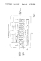
System Overview (FIG. 1)
The present invention is built-in self-test system for very large-scale integrated circuit chips. As illustrated in FIG. 1, built-in self-test (BIST) system 10 is fabricated on a very large-scale integrated (VLSI) circuit chip 12 which includes main logic function 14. It is to be noted that main logic function 14 will typically include tens or even hundreds of thousands of electronic devices such as transistors or FETs, and comprise a major portion of the surface area of integrated circuit chip 12. BIST system 10 can be adapted for use with all types of main logic function 14. Although represented in block form in FIG. 1, main logic function 14 can include gate arrays, memory chips, or other custom integrated circuit chips. In a preferred embodiment, BIST system 10 is adapted for use with a 20K CMOS gate array.
Integrated circuit chip 12 includes a plurality (238 in one embodiment) of input pins 18 on which input data is received. Main logic function 14 is connected to receive the input data through a plurality of input lines 20. Output data produced by main logic function 14 is outputted from integrated circuit 12 on output pins 22 through output lines 24. As shown, each output line 24 includes sections 24A, 24B, and 24C. In one embodiment, integrated circuit chip 12 has 140 output lines 24 and output pins 22. A plurality of output buffers 26, one on each output line 24 (best shown in FIG. 8), interface output line sections 24B with sections 24C. Main logic function 14 can be electrically disconnected, or isolated, from input pins 18 and output pins 22 by means of transmission gates 28 and 30, respectively. Transmission gates 30 interface output line sections 24A and 24B. Transmission gates 28 and 30 are under the direct control of BIST system 10, as will be described subsequently in greater detail.
As shown in FIG. 1, BIST system 10 includes control register 32, test data transfer logic 34, input register and operand generator 36 (hereafter referred to as input register 36), output register and checksum logic 38 (hereafter referred to output register 38), test data output control logic 40, and control logic 42. Control logic 42 is connected to receive a system clock (SYS CLK) signal from SYS CLK input pin 44, a test clock enable (TCE) signal on TCE input pin 46, and a test strobe (TS) signal from TS input pin 48. Various control signals produced by control logic 42 are supplied to control register 32, test data transfer logic 34, input register 36, output register 38, and test data output control logic 40 as shown.
Control register 32 is connected to receive test data, in serial format, through test data input (TDI) pin 50. Control register clock (CLK) and ENABLE control signals are received from control logic 42. In response to these control signals, test data is serially shifted through control register 32, with function codes included therein being produced as control signals at control nodes N0-N23. As schematically illustrated in FIG. 1, the control signals from control nodes N0-N23 are distributed throughout integrated circuit 12. The function of control signals at control nodes N0-N23 will be described in subsequent portions of this specification.
Input register 36 is connected to receive serial test data from test data transfer logic 34, and an input register clock (CLK) signal from control logic 42. Test data transfer logic 34, under the control of a test data select (TDS) control signal produced by control logic 42, causes test data to be supplied to input register 36 either directly from TDI pin 50, or from control register 32. Input register 36 is also connected for parallel test data transfer with input lines 20 through transmission gates 52.
Output register 38 is connected to receive serial test data from input register 36, and an output register clock (CLK) signal from control logic 42. Output register 38 is also connected for parallel, bi-directional test data transfer with output lines 24 through transmission gates 54 and 56. As shown, output register 38 can transfer data through transmission gate 54 to output lines 24 at a point intermediate transmission gates 30 and output buffers 26. Test data from output lines 24 at a point either between transmission gates 30 and output buffers 26, or between output buffers 26 and output pins 22, is received by output register 38 through transmission gates 56.
Test data output control logic 40 controls the transfer of test data from BIST system 10 to test data output (TDO) pin 60 in response to control signals received from control nodes N0 and N1 of control register 32. In addition to test data from output register 38, test data output control logic 40 can supply alternate test data from main logic function 14 (as schematically illustrated by node A), a copy of the SYS CLK signal, or an internal test frequency signal such as that produced by oscillator 62, to TDO pin 60.
Control Logic 42 and Test Data Transfer Logic 34 (FIG. 2)
Control logic 42 and test data transfer logic 34 are schematically illustrated in FIG. 2. Control logic 42 includes buffers 70, 72, and 74, latches 76 and 78, flip-flop 80, and NAND gates 82 and 84. Latches 76 and 78 are preferably positive level triggered D-type latches, both of which have a data or D input terminal, and a clock or C input terminal. Latch 76 has a non-inverting output terminal 86 and an inverting output terminal 88, while latch 78 has a non-inverting output terminal 90.
Latches 76 and 78 are common circuit elements, and their operation is well known. The logic state (i.e. a "LOW" or logic 0 logic state, or a "HIGH" or logic 1 state) of data produced by on their non-inverting output terminals 86 and 90 will follow, or have the same logic state as, data received on the D input terminal so long as a signal received at the C input terminal has the logic 1 state. When the signal applied to the C input terminal is raised, or switched from the logic 0 state to a logic 1 state, the logic state of data then present at the D input terminal is latched, or fixed, at non-inverting output terminals 86 and 90. Subsequent changes to the logic state of the data signal received on the D input terminal will be ignored so long as the signal received at the C input terminal remains at the logic 1 state. The data signal produced on inverting output terminal 88 of latch 76 will always have a logic state opposite that of non-inverting output terminal 86.
Flip-flop 80 is preferrably a positive transition edge triggered D-type flip-flop. As shown in FIG. 2, flip-flop 80 has a data or D input terminal, a clock or C input terminal, and a non-inverting output terminal 92. When the signal received at the C input terminal of flip-flop 80 is raised, or switched from a logic 0 state to a logic 1 state, the logic state of the data signal then present at the D input terminal is strobed, or fixed, onto non-inverting output terminal 92. A logic state of the signal on non-inverting output terminal 92 can change states in this manner only when the signal applied to the C input terminal is raised.
NAND gate 82 is a 3-input gate having first, second, and third input terminals 84, 96, and 98, respectively, and output terminal 100. NAND gate 84 is a 2-input gate having first and second input terminals 102 and 104, respectively, and output terminal 106. NAND gates 82 and 84 are common circuit elements which perform a logical NAND operation on signals received at their respective input terminals. Simply put, output terminals 100 and 106 of NAND gates 88 and 84, respectively, will be at logic 1 state unless all input terminals of the respective gates receive a signal having a logic 1 state, in which case output terminals 100 and 106 will be at a logic 0 state.
Buffers 70, 72 and 74 have input terminals 67, 69, and 71, respectively, and output terminals 73, 75, and 77, respectively. Buffers 70, 72, and 74 produce output signals having the same logic states as the signals received at their input terminals.
As shown in FIG. 2, the system clock (SYS CLK) signal is applied, through buffer 74, to first input terminals 94 and 102 of NAND gates 82 and 84, respectively, and to the C input terminal of latches 76, 78, and flip-flop 80. The test strobe (TS) signal is applied to the D input terminal of latch 76 through buffer 70. Latch 76 latches the logic state of the TS signal onto its output terminals 86 and 88 when SYS CLK raises from the logic 0 to the logic 1 sate, thereby producing a "latched" TS signal. The latched TS signal from non-inverting output terminal 86 is applied to the D input terminal of flip-flop 80, from which it is strobed to non-inverting output terminal 92 upon a succeeding positive transition of SYS CLK. As shown in FIG. 2, the latched TS signal is a control signal which is applied to the ENABLE control terminal of control register of 32. The logic state of the control register ENABLE signal will follow that of TS after one cycle of SYS CLK.
The test clock enable (TCE) signal is applied to the D input terminal of latch 78 through buffer 72. Latch 78 latches the logic state of the TCE signal when SYS CLK is raised from the logic 0 state to the logic 1 state, thereby producing a "latched" TCE signal on its non-inverting output terminal 90. As shown, the latched TCE signal is applied to second input terminal 96 and 104 of NAND gates 82 and 84, respectively. The latched TCE signal is gated with the SYS CLK signal by NAND gate 84. As shown, the signal present on output terminal 106 of NAND gate 84 is applied to the clock (CLK) input terminal of input register 36, output register 38, and test data output control logic 40.
Third input terminal 98 of NAND gate 82 is connected to receive the latched TS signal from inverting output terminal 88 of latch 76. NAND gate 82 thereby gates the latched TS and TCE signals with the SYS CLK signal. The gated TS and TCE signals are output NAND gate 82 at output terminal 100, and applied to the clock (CLK) terminal of control register 32 as shown.
Test data select logic 34 includes inverter 110, first and second transmission gates 112 and 114, respectively, and buffer 116. Transmission gate 112 has an input terminal 117, an output terminal 118, a non-inverting control terminal 120, and inverting control terminal 122. Second transmission gate 114 has an input terminal 124, an output terminal 126, a non-inverting control terminal 128, and an inverting control terminal 130. Inverter 110 has an input terminal 109, and an inverting output terminal 111.
Inverter 110 and transmission gates 112 and 114 are common circuit elements, the operation of which are well known. Inverter 110 inverts the logic state of the signal received at its input terminal 109. A signal having a logic 1 state at input terminal 109, for example, would be converted to a signal having a logic 0 state at output terminal 111.
Transmission gates 112 and 114 function in an identical manner. The following description of transmission gate 112 therefore applies to transmission gate 114, and other transmission gates yet to be described. Transmission gate 112 functions much like a switch and controls the transmission of signals between its input terminal 117 and output terminal 118 in response to control signals received at its control terminals 120 and 122. Transmission gate 112 is driven to its OFF state thereby electrically disconnecting input terminal 117 from output terminal 118, and prohibiting the flow of data therebetween, when a signal having a logic 1 state is applied to inverting control terminal 122 and a signal having a logic 0 state is applied to non-inverting control terminal 120. When a signal having a logic 0 state is applied to inverting control terminal 122, and a signal having a logic 1 state is applied to non-inverting control terminal 120, transmission gate 112 will be in its ON state. In its ON state, input terminal 117 is electrically connected to output terminal 118, and data transfer permitted.
As shown in FIG. 2 the latched TS signal from inverting output terminal 88 of latch 76 is applied to test data transfer logic 34 as a test data select (TDS) signal. Input terminal 109 of inverter 110, inverting control terminal 130 of transmission gate 114, and non-inverting control terminal 120 of transmission gate 112 are all connected to receive the latched TS signal. Output terminal 111 of inverter 110 is connected to non-inverting control terminal 128 of transmission gate 114, and inverting control terminal 122 of transmission gate 112. Input terminal 117 of transmission gate 112 is connected to receive test data from control register 32. Input terminal 124 of transmission gate 114 is connected to receive test data directly from TDI pin 38. Output terminals 118 and 126 of transmission gates 112 and 114, respectively, are both applied to input register 36 through buffer 116.
When the TDS signal (latched test strobe signal) received by test data transfer logic 34 has logic 1 state, transmission gate 112 will be ON, while transmission gate 114 will be OFF. Test data from control register 32 will thereby be propogated to input register 36. When the test data select signal has a logic 0 state, transmission gate 114 will be ON, while transmission gate 112 will be OFF. Test data from test data input pin 38 will thereby be propogated to input register 36, bypassing control register 32.
Latches 76, 78, and flip-flop 80 greatly simplify the job of a logic designer designing main logic function 14 and test procedures for BIST system 10. TS and TCE signals need no longer be accurately synchronized, or tuned, with the system clock signal. By latching the TS and TCE signals, with the system clock signal, "runt" pulses, long or short set up paths, and other timing violations which can cause errors in the system operation can be reduced. This improvement is especially significant when it is understood that at the extremely high speeds at which BIST system 10 operates, it was previously virtually impossible for the logic designer to accurately predict and account for all possible timing violations. By facilitating the logic designer's job, latches 76, 78, and flip-flop 80 effectively reduce overall chip testing costs.
Control Register 32 (FIGS. 3 and 4)
FIG. 3 is a schematic representation of control register 32. In the embodiment shown, control register 32 is a 24 bit (i.e. bits 0-23) shift register and is formed by a series arrangement of static flip-flops 150. Each flip-flop 150 has a data or D input terminal, a clock or C input terminal, and an output terminal 152. Test data from TDI pin 50 is inputted the D input terminal of bit 0 flip-flop 150 through buffer 160. With the exception of bit 23, output terminal 152 of each flip-flop 150 is connected to the D input terminal of the succeeding flip-flop 150. Output terminal 152 of bit 23 flip-flop 150 is connected, through buffer 162, to test data transfer logic 34. The C input terminal of each flip-flop 150 is connected to receive the control register clock signal (CLK) produced by control logic 42.
Associated with each flip-flop 150 is NAND gate 154. Each NAND gate 154 has a first input terminal 158 connected to output terminal 152 of its respective flip-flop 150, and a second input terminal 156 connected to receive the control register ENABLE signal produced by control logic 42. An output of each NAND gate 154 is a control node. Control nodes N0-N23 are associated with bits 0-23, respectively. Control nodes N0-N23 are connected to various circuit elements of BIST system 10, as illustrated in FIG. 1.
Buffers 160, 162, and NAND gates 154 are common circuit elements. The operation NAND gates such as 154 has been previously described. Flip-flops 150 of control register 32 are all static flip-flops, and are preferrably negative edge triggered. A logic state of a data signal present at the D input terminal of each flip-flop 150 will be strobed to the respective output terminal 152 upon negative (i.e. logic 1 to logic 0) transitions of the control register clock signal.
Test data is serially shifted through bits 0-23 of control register 32 at a rate of 1 bit per cycle of the control register clock signal. After 24 cycles of the control register clock signal, for example, the logic state of the data signal originally present at the D input terminal of bit 0 flip-flop 150 will have been shifted to output terminal 152 of bit 23 flip-flop 150. Control register 32 is "loaded" by serially shifting test data including function codes through flip-flops 150. The function code is representative of a desired operational state of BIST system 10, the and is "enabled" when the control register ENABLE signal is raised from a logic 0 state to a logic 1 state (i.e. when TS is raised). Once enabled, individual bits of the function code are passed to control nodes N0-N23 through respective NAND gates 154, and used as control signals. Circuit elements controlled by the control signals on nodes N0-N23 are thereby driven to their desired operational state. While TS is at a logic 1 state the control register clock is blocked (i.e. maintained at a logic 0 state) freezing the function code in control register 32. As previously discussed, TDI pin 50 will also be connected directly to input register 36, bypassing control register 32, so that the function code in control register 32 will remain valid while test data is being shifted, if desired.
In the embodiment shown, control bits N0-N9 are dedicated to the control of various gating functions required to implement all test modes of BIST system 10. Remaining control nodes N10-N23 are "spare" bits that a logic designer can use to control main logic function 14 and thereby enhance its testability. The functions of bits 0-9 and their respective control nodes N0-N9 are described in FIG. 4. These functions are also illustrated in FIG. 1 by the interconnections of control nodes N0-N9 with the circuit elements of BIST system 10. The states of all control nodes are arranged so that when the control register ENABLE signal is dropped to a logic 0 state, (i.e. when TS is dropped to a logic 0 state) all test and maintenance operations within BIST system 10 are disabled, and main logic function 14 left undisturbed for normal operation. Control nodes N0-N23 are all active "LO" (i.e., when the control signal thereon has logic 0 state).
The static flip-flops 150 used to implement control register 32, unlike alternative designs, permit data to be maintained, or stored, at output terminals 152 irrespective of the logic state of the control register clock signal (i.e. logic states of TS, TCE, and SYS CLK). In other words the logic state of the data signal at output terminal 152 of flip-flops 150 will remain constant, and thereby be stored, if the control register clock is stopped at either a logic 1 or a logic 0 level. TS and TCE need no longer be carefully tuned with respect to the system clock signal. Similarly, the logic designers attention need no longer be focused on SYS CLK. Design constraints imposed upon logic designers are thereby removed permitting greater flexibility in designing main logic function 14 for testibility.
Input Register 36 (FIG. 5)
Input register and operand generator 36 (input register 36) is schematically represented in FIG. 5. In the embodiment shown, input register 36 is a 238-bit (i.e. bits 0-237) shift register formed by a series arrangement of static flip-flops 170. Each flip-flop 170 has a data or D input terminal, a clock or C input terminal, and an output terminal 180. Test data from test data transfer logic 34 is inputted to the D input terminal of bit 0 flip-flop 170. Output terminal 180 of bit 0-237 flip-flops 170 is connected to the D input terminal of the following flip-flop 170. Output terminal 180 of bit 237 flip-flop 170 is connected to output register 38. The C input terminal of each flip-flop 170 is connected to receive the input register clock (CLK) signal from control logic 42. Each flip-flop 170 is associated with one of input lines 20, and has its D input terminal operatively connected to the respective input line 20 through transmission gates 52 as illustrated.
Input register 36 also includes operand generator logic 172, and serial data path control logic 174. Operand generator logic 172 receives a control signal from control node N4 of control register 32, and is interfaced with bit 0-237 flip-flops 170 as illustrated generally by bus 176. Serial data path control logic 174 receives a control signal from control node N2 of control register 32, and is interfaced with bit 0-237 flip-flops 170 as illustrated generally by bus 178.
When control register 32 is loaded with an appropriate function code and enabled, operand generator logic 172 will repeatedly produce test operands from a non-zero starting point or "seed". These test operands are input bit 0-237 flip-flops 170 in a parallel format by bus 176. Under normal conditions, serial data path control logic 174 causes flip-flops 170 to be interconnected as a shift register for serial test data transfer between test data transfer logic 34 and output register 38. When control register 32 is loaded with an appropriate function code and enabled, serial data path control logic 174 causes bit 0-237 flip-flops 170 to be connected for parallel test data transfer with input lines 20 through transmission gates 52.
Operands produced by operand generator logic 172 can be applied in parallel to input lines 20 (and thereby into main logic function 14) when input pins 18 are isolated from main function 14 by transmission gates 28. Data on input lines 20 can also be received, in a parallel format, by bit 0-237 flip-flops 170 through transmission gates 52. Logic states of signals at input pins 18 can thereby be directly observed during system testing. Main logic function 14 can also be directly controlled during various test procedures by test data from input register 36.
All flip-flops 170 of input register 36 are static flip-flops offering the same advantages to BIST system 10 as those already described with reference to control register 32. Flip-flops 170 are preferrably negative edge triggered flip-flops which operate in a manner indentical to flip-flops 150 of control register 32.
Output Register 38 (FIG. 6)
Output register 38 is schematically represented in FIG. 6. In the embodiment shown, output register 38 is a 140 bit (ie. bits 0-139) shift register formed by a series arrangement of static flip-flops 182. Each of bit 0-139 flip-flops 182 is associated with one of output lines 24. Each flip-flop 182 has a data or D input terminal, a clock or C input terminal, and an output terminal 184. Test data from input register 36 is inputted to the D input terminal of bit 0 flip-flop 182. Output terminal 184 of bit 0-138 flip-flops 182 are connected to the D input terminal of the following flip-flop 182. Output terminal 184 of bit 139 flip-flop 182 is connected to test data output control logic 40. The C input terminal of each flip-flop 182 is connected to receive the output register clock (CLK) signal from control logic 62. The D input terminal of each bit 0-139 flip-flop 182 is also operatively connected to one of output line sections 24B through transmission gates 54 and 56, as illustrated.
Control register 36 also includes checksum logic 186 and serial/parallel data path control logic 188. Checksum logic 186 is interfaced with each bit 0-139 flip-flop 182, as illustrated generally by bus 190. Serial/parallel data path control logic 188 is connected to receive a control signal from control node N5 of control register 132, and is interfaced with bit 0-239 flip-flops 182, as illustrated generally by bus 192. When loaded with an appropriate function code, control register 32 causes serial/parallel data path control logic 188 to conenct flip-flops 182 as a shift register for serial data transfer between input register 36 and test data output control logic 40.
When loaded with other function codes, control register 32 causes serial/parallel data path control logic 188 to interconnect bit 0-139 flip-flops 182 for bi-directional parallel data transfer with output line sections 24B. Having serially loaded output register 38 with desired test data, and loading control register 32 with an appropriate function code, output pins 22 can be driven through transmission gates 54 and output buffers 26 to logic states represented by the test data. Other function codes will cause data from output lines 24 to be transferred, in parallel, through transmission gates 56 to bit 0-139 flip-flops 182 of output register 38. As illustrated in FIG. 1, this output data can come from output line sections 24B at a point intermediate transmission gates 30 and output buffers 26, or from a point intermediate output buffers 26 and output pins 22 (i.e., from output line sections 24C).
Operating output register 38 in a manner described above, the response of main logic function 14 to test operands produced by operand generator logic 172 of input register 36 can be accumulated into a checksum by checksum logic 186. This checksum is computed by half-adding current contents of output register 38 with current data on output lines 24. The checksum result is then reloaded into output register 38, and serially shifted to test data output control logic 40.
All flip-flops 182 of output register 38 are static flip-flops, offering the same advantages to BIST system 10 as the static flip-flops of control register 32 and input register 36. In the embodiment shown, flip-flops 182 are negative edge triggered flip-flops. The operation of devices of this type has been previously described.
Test Data Ouput Control Logic 40 (FIG. 7)
A preferred embodiment of test data output control logic 40 is schematically illustrated in FIG. 7. Output control logic 40 functions as a multiplexer which, under the control of control register 32, selects test data from one of four possible inputs for transfer to TDO pin 60. As shown in FIG. 7, output control logic 40 is connected to receive test data from output register 38, alternate test data from main logic function 14 (as illustrated by node A), the system clock signal (SYS CLK), and the internal test frequency signal produced by oscillator 62. In one preferred embodiment, oscillator 62 is formed on integrated circuit chip 12 by a ring of inverters. Control register 32, through control signals on control nodes N0 and N1, controls which of these four possible forms of test data will be transferred to TDO pin 60.
As shown in FIG. 7, test data output control logic 40 is formed by transmission gates 210, 212, 214, 216, and 218, flip-flop 220, inverters 222, 224, 226, and 228, NAND gate 230, and NOR gate 232. Transmission gates 210-218, inverters 222-228, NAND gate 230, and flip-flop 220 are functionally identical to their counterparts described with reference to control logic 42 and control register 32. NOR gate 232 performs a logical NOR operation, producing an output signal having a logic 0 state at its output terminal 234 when the signal at either of its input terminals 236 or 238 has a logic 1 state.
Input terminal 240 of transmission gate 210 is connected to receive the alternate test data from node A of main logic function 14. Input terminal 242 of transmission gate 212 is connected to receive test data from output register 38. Input terminal 244 of transmission gate 216 is connected to receive SYS CLK. Input terminal 246 of transmission gate 218 is connected to receive the internal test frequency signal from oscillator 62. Input terminal 248 of transmission gate 214 is connected to output terminal 250 of flip-flop 220. Output terminals 252 and 254 of transmission gates 210 and 212, respectively, are connected to the D input terminal of flip-flop 220. Output terminals 256, 258, and 260 of transmission gates 214, 216, and 218, respectively are connected to test data output pin 60.
Inverting control terminal 262 of transmission gate 210, non-inverting input terminal 264 of transmission gate 212, input terminal 266 of inverter 222, input terminal 268 of NAND gate 230, and input terminal 238 of NOR gate 232 are all connected to receive the control signal present at control node N1 of control register 32. Non-inverting control terminal 270 of transmission gate 214, input terminal 272 of inverter 224, and input terminal 236 of NOR gate 232 are all connected to receive the control signal present at control node N0 of control register 32.
Inverter 228 has an input terminal 270 connected to output terminal 234 of NOR gate 232, and to non-inverting control terminal 272 of transmission gate 218. Output terminal 274 of inverter 228 is connected to inverting control terminal 276 of transmission gate 218. NAND gate 230 has an input terminal 278 connected to output terminal 280 of inverter 224, and an output terminal 282 connected to input terminal 284 of inverter 226 and to inverting control terminal 286 of transmission gate 216. Output terminal 280 of inverter 224 is connected to inverting control terminal 288 of transmission gate 214. Output terminal 290 of inverter 226 is connected to non-inverting control terminal 292 of transmission gate 216. Non-inverting control terminal 294 of transmission gate 210, and inverting control terminal 296 of transmission gate 212 are both connected to output terminal 298 of inverter 222. A clock or C input terminal of flip-flop 220 is connected to receive the test data output control logic clock (CLK) signal produced by control logic 42.
Control signals received from control nodes N0 and N1 of control register 32 are decoded by test data output control logic 40 to uniquely and actively select test data which will be supplied to TDO pin 60. When control register 32 is loaded with a function code which drives control nodes N0 and N1 to logic 1, 1 states respectively, when enabled, transmission gates 212 and 214 are switched ON, while transmission gates 210, 216, and 218 are switched OFF. Test data from output register 38 is thereby transferred through transmission gate 212 and clocked by flip-flop 220 through transmission gate 214 to TDO pin 60. This is the "normal" test data output mode which can occur when the test strobe signal, and therefore the control register ENABLE signal, has a logic 0 state.
When control register 32 is loaded with a function code which drives control nodes N0 and N1 to logic 1, 0 states respectively, when enabled, transmission gates 210 and 214 are switched ON, while transmission gates 212, 216, and 218 are switched OFF. Alternate test data received from main logic function 14 is thereby transferred through transmission gate 210, and clocked by flip-flop 220 through transmission gate 214 to test data output pin 60.
Transmission gate 216 will be switched ON, and transmission gates 210, 212, 214, and 218 switched OFF, when control register 32 is loaded with a function code which causes control nodes N0 and N1 to have logic 0, 1 states respectively, when enabled. The system clock signal will thereby be transferred through transmission gate 216 to test data output pin 60.
Transmission gate 218 will be switched ON, and transmission gates 210-216 switched OFF, when control register 32 is loaded with a function code which causes control nodes N0 and N1 to have logic 0, 0 states respectively, when enabled. The internal test frequency signal from oscillator 62 will thereby be transferred through transmission gate 218 to test data output pin 60.
By using dedicated control nodes within control register 32 to select different types of data to be sent out to test data output pin 60, the logic designer is no longer required to use other available control nodes for this function. They therefore remain available for other test functions. The logic designer's task of designing tests to be executed with BIST system 10 is also greatly simplified, since he or she is no longer required to actively block those test data paths which are not selected.
Output Buffers 26 (FIG. 8)
Output buffers 26 are schematically represented in FIG. 8. As shown, output line sections 24B and 24C are interfaced by output buffers 26. Each output buffer 26 has a data input terminal 240 connected to its respective output line section 24B. An output terminal 242 of each output buffer 26 is connected to its respective output pin 22 through an output line section 24C. Each buffer 26 also includes an ENABLE input terminal which is adapted to be interconnected by the logic designer to points within main logic function 14. Output buffers 26 are standard tri-state buffers, having ON and OFF states controlled by a signal received at the ENABLE input terminal. When enabled, or ON, buffers 26 transfer data received at their input terminal 240 to their output terminal 242. When disabled, or OFF, output terminals 242 are driven to a high impedance state, electrically isolating input terminal 240 from output terminal 242.
In addition to the ENABLE control terminal which is available for interconnection at the logic designer's discretion, each output buffer 26 can be directly controlled by control register 23. A Force Off (FOF) control terminal 244 of each output buffer 26 is connected to control node N8 of control register 32 through buffer 241. A Force Active (FAC) control terminal 246 of each output buffer 26 is connected to control node N9 of control register 32 through inverter 243.
When control register 32 is loaded with a function code which, when enabled, causes control node N8 to have a logic 0 state, all output buffers 26 are forced OFF, or into their tri-state, high impedance mode. Output terminal 242 of each output buffer 26 is thereby electrically isolated from its respective input terminal 240. When control register 32 is loaded with a function code which, when enabled, causes control node N9 to have a logic 0 state, all output buffers are forced ON, or active. Output buffers 26 are thereby operated in their normal mode, with the logic state at their output terminal 242 being determined by the logic state of data at their data input terminal 240. The FAC signal received from function node N9 will override the FOF signal received at function node N8 if both are selected by control register 32.
The FAC and FOF control terminals on output buffers 26 permit the logic designer to drive output pins 22 from the output register 38 through function codes entered into control register 32. This greatly simplifies the logic designer's task when designing tests since he or she is no longer required to know the particular operation of a circuit being tested. Test design is thereby made easier, and less expensive.
Although the present invention has been described with reference to preferred embodiments, workers skilled in the art will recognize that changes may be made in form and detail without departing from the spirit and scope of the invention.

Claims (30)

What is claimed is:
1. An LSI circuit including:
main logic function means for performing digital logic operations; and
built-in test system means interconnected with the main logic function means for performing dynamic tests of main logic function operation, the built-in test system means including:
test data input means for receiving test data in a serial format;
clock input means for receiving a clock signal which switches between first and second logic states; and
shift register means responsive to the test data input means and the clock input means for storing and serially transferring test data, the shift register means comprising a series of static flip-flops which enable data stored therein to be maintained irrespective of the logic state of the clock signal.
2. The LSI circuit of claim 1 wherein the shift register means includes a control register responsive to the test data input means and the clock input means for serial test data transfer, and for producing test system control signals, the control register comprising a plurality of static flip-flops interconnected in a series arrangement.
3. The LSI circuit of claim 2 wherein the shift register means further includes an input shift register responsive to the clock input means, the control register, and the main logic function means for serial test data transfer with the control register, and for parallel test data transfer with the main logic function means, the input shift register comprising a plurality of static flip-flops interconnected in a series arrangement.
4. The LSI circuit of claim 3 wherein the shift register means further includes an output shift register responsive to the clock input means, the input shift register, and the main logic function means for serial test data transfer with the input shift register, and for parallel test data transfer with the main logic function means, the output shift register comprising a plurality of static flip-flops interconnected in a series arrangement.
5. The LSI circuit of claim 1 wherein the shift register means comprise a plurality of static D-type flip-flops interconnected in a series arrangement.
6. The LSI circuit of claim 5 wherein the flip-flops are negative edge triggered D-type flip-flops.
7. An LSI circuit, including:
main logic function means for performing digital logic operations; and
built-in test system means interconnected with the mian logic function means for performing dynamic tests of main logic function operation, the built-in test system means including:
test data input means for receiving test data in a serial format;
test strobe input means for receiving a test strobe signal;
test clock enable input means for receiving a test clock enable signal;
system clock input means for receiving a system clock signal;
test strobe latch means responsive to the test strobe input means and the system clock input means for producing a latched test strobe signal;
test clock enable latch means responsive to the test clock enable input means and the system clock input means for producing a latched test clock enable signal;
first logic gate means responsive to the system clock input means, the test strobe latch means, and the test clock enable latch means for producing a control register clock signal as a logical function of the system clock signal, the latched test strobe signal, and the latched test clock enable signal; and
a control register responsive to the test data input means and the first logic gate means for serially transferring test data when clocked by the control register clock signal, and for producing test system control signals.
8. The LSI circuit of claim 7 wherein:
the test strobe latch means includes a first D-type latch having a D input terminal responsive to the test strobe input means, a C input terminal responsive to the system clock input means, a non-inverting output terminal, and an inverting output terminal, the first D-type latch producing the latched test strobe signal at the non-inverting and inverting output terminals; and
the test clock enable latch means includes a second D-type latch having a D input terminal responsive to the test clock enable input means, a C input terminal responsive to the system clock input means, and a noninverting output terminal, the second D-type latch producing the latched test clock enable signal at the output terminal.
9. The LSI circuit of claim 8 wherein:
the first D-type latch is a positive level triggered latch which latches a logic state of the test strobe signal thereby producing the latched test strobe signal on negative transitions of the system clock signal; and
the second D-type latch is a positive level triggered latch which latches a logic state of the test clock enable signal thereby producing the latched test clock enable signal on negative transitions on the system clock signal.
10. The LSI circuit of claim 9 wherein the first logic gate means comprises a first NAND gate having a first input terminal responsive to the first D-type latch, a second input terminal responsive to the second D-type latch, a third input terminal responsive to the system clock input means, and an output terminal, the first NAND gate performing a logical NAND operation on the latched test strobe signal, the latched test clock enable signal, and the system clock signal, and producing the control register clock signal at its output terminal.
11. The LSI circuit of claim 10 wherein:
the first input terminal of the first NAND gate is connected to the inverting output terminal of the test strobe D-type latch; and
the second input terminal of the first NAND gate is connected to the non-inverting output terminal of the test clock enable D-type latch.
12. The LSI circuit of claim 8 wherein:
the control register includes an enable input terminal for receiving a control enable signal for enabling test system control signals produced by the control register; and
the built-in test system means further includes a D-type flip-flop having a D input terminal responsive to the first D-type latch means, a C input terminal responsive to the system clock input means, and an output terminal, the D-type flip-flop producing the control enable signal at its output terminal by strobing the latched test strobe signal to the output terminal on transitions of the system clock signal.
13. The LSI circuit of claim 12 wherein the D-type flip-flop is a positive transition edge triggered flip-flop which produces the control enable signal by strobing a logic state of the latched test strobe signal to the output terminal on positive transitions of the system clock signal.
14. The LSI circuit of claim 13 wherein the D input terminal of the flip-flop is connected to the non-inverting output terminal of the first D-type latch.
15. The LSI circuit of claim 8 wherein:
the built-in test system further includes:
shift register means responsive to the control register and the main logic function means for serial test data transfer with the control register, and parallel test data transfer with the main logic function means, when clocked by a shift register clock signal; and
second logic gate means responsive to the system clock input means and the second D-type latch for producing the shift register clock signal as a logical function of the system clock signal and the latched test clock enable signal.
16. The LSI circuit of claim 15 wherein the second logic gate means comprises a second NAND gate having a first input terminal responsive to the system clock input means, a second input terminal responsive to the second D-type latch, and an output terminal, the NAND gate performing a logical NAND operation on the system clock signal and the latched test clock enable signal thereby producing the shift register clock signal at its output terminal.
17. An LSI circuit, including:
main logic function means for performing digital logic operations; and
built-in test system means interconnected with the mian logic function means for performing dynamic tests of main logic function operation, the built-in test system means including:
test data input means for receiving test data in a serial format;
test clock enable input means for receiving a test clock enable signal;
system clock input means for receiving a system clock signal;
test clock enable latch means responsive to the test clock enable input means and the system clock input means for producing a latched test clock enable signal;
logic gate means responsive to the system clock input means and the test clock enable latch means for producing a shift register clock signal as a logical function of the system clock signal and the latched test clock enable signal; and
shift register means responsive to the test data input means, the main logic function means and the logic gate means for serial test data transfer with the test data transfer with the test data input means and parallel test data transfer with the main logic function means, when clocked by the shift register clock signal.
18. The LSI circuit of claim 17 wherein the test clock enable latch means includes a D-type latch having a D input terminal responsive to the test clock enable input means, a C input terminal responsive to the system clock input means, and an output terminal, the D-type latch producing the latched clock enable signal at the output terminal.
19. The LSI circuit of claim 18 wherein the D-type latch is a positive level triggered latch which latches a logic state of the test clock enable signal thereby producing the latched test clock enable signal on negative transitions of the system clock signal.
20. The LSI circuit of claim 19 wherein the logic gate means comprises a NAND gate having a first input terminal responsive to the D-type latch, a second input terminal responsive to the system clock input means, and an output terminal, and NAND gate performing a logical NAND operation on the latched test clock enable signal and the system clock signal, and producing the shift register control signal at its output terminal.
21. An LSI circuit including:
main logic function means for performing digital logic operations and including an internal signal node at which alternate test data is present; and
built-in test system means interconnected with the main logic function means for performing dynamic tests of main logic function operation, the built-in test system means including:
test data input means for receiving test data in a serial format;
test data output means from which test data is outputted;
control register means responsive to the test data input means for serial test data transfer, and for producing test system control signals including an alternate test data select signal and a normal test data select signal;
shift register means responsive to the control register means and the main logic function means for serial test data transfer with the control register means, and parallel test data transfer with the main logic function means; and
test data output control means responsive to the shift register means, the main logic function means, and the control register means, the test data output control means causing alternate test data from the internal signal node of the main logic function means to be supplied to the test data output means when the control register means produces the alternate test data select signal, and causes test data from the shift register means to be supplied to the test data output means when the control register means produces the normal test data select signal.
22. The LSI circuit of claim 21 wherein:
the built-in test system means further includes system clock input means for receiving a system clock signal;
the test system control signals produced by the control register means further include a system clock test data select signal; and
the test data output control means is responsive to the system clock input means and causes the system clock signal to be supplied to the test data output means when the control register means produces the system clock test data select signal.
23. The LSI circuit of claim 21 wherein:
the built-in test system means further includes oscillator means for producing an internal test frequency signal;
the test system control signals produced by the control register means further include a test frequency test data select signal; anda
the test data output control means is responsive to the oscillator means and causes the internal test frequency signal to be supplied to the test data output means when the control register means produces the test frequency test data select signal.
24. The LSI circuit of claim 23 wherein:
the control register means produces the test system control signals as a two bit control signal having a digital state representative of selected test data; and
the test data output control means includes a digital multiplexer responsive to the internal signal node, the shift register means, the system clock input means and the oscillator means, for decoding the two bit control signal and supplying test data represented thereby to the test data output means.
25. An LSI circuit, including;
main logic function means for performing digital logic operations; and
built-in test system means interconnected to the main logic function means for performing dynamic tests of main logic function means operation, the built-in test system means including:
test data input means for receiving test data in a serial format;
system clock input means for receiving a system clock signal which switches between first and second logic states;
test strobe input means for receiving a test strobe signal;
test clock enable input means for receiving a test clock enable signal;
test strobe latch means responsive to the test strobe input means and the system clock input means for producing a latched test strobe signal by latching a logic state of the test strobe signal on transitions of the system clock signal;
test clock enable latch means responsive to the test clock enable input means and the system clock input means for producing a latched test clock enable signal by latching a logic state of the test clock enable signal on transitions of the system clock signal;
first logic gate means responsive to the test strobe latch means, the test clock enable latch means, and the system clock means, for gating the latched test strobe signal and the latched test clock enable signal with the system clock signal and producing a control register clock signal;
second logic gate means responsive to the test clock enable latch means and the system clock input means for gating the latched test clock enable signal with the system clock signal and producing a shift register clock signal;
control register means responsive to the test data input means and the first logic gate means for serial test data transfer when clocked by the control register clock signal, and for producing test system means control signals, the control register means comprising static flip-flops interconnected in a series arrangement; and
shift register means responsive to the control register means, the second logic gate means, and the main logic function means for serial test data transfer with the cotnrol register means, and for parallel test data transfer with the main logic function means, when clocked by the shift register clock signal, the shift register means comprising a plurality of static flip-flops interconnected in a series arrangement.
26. The LSI circuit of claim 25, wherein:
the built-in test system means further includes test strobe flip-flop means responsive to the test strobe latch means and the system clock input means for producing a control register enable signal by strobing a logic state of the latched test strobe signal on transistions of the system clock signal; and
the control register means is responsive to the test strobe flip-flop means for enabling the test system control signals upon receipt of the control register enable signal.
27. The LSI circuit of claim 25, wherein:
the main logic function means further includes an internal test sigal node at which alternate test data is present;
the control register means of the built-in test system means produces a test data select signal representative of selected test data; and
the built-in test system means further includes:
test data output means from which test data is outputted;
test data output multiplexer means responsive to the internal signal node of the main logic function means, the control register means, and the shift register means, for decoding the test data select signal and supplying test data represented thereby to the test data output means, the test data output multiplexer means supplying alternate test data from the main logic function means to the test data output means when the test data select signal is representative of alternate test data, and supplying normal test data from the shift register means to the test data output means when the test data select signal is representative of normal test data.
28. The LSI circuit of claim 27 wherein:
the test data output multiplexer means is responsive to the system clock input means and supplies the system clock signal to the test data output means when the test data select signal is representative of system clock test data.
29. The LSI circuit of claim 28 wherein:
the built-in test system means further includes oscillator means for producing an internal test frequency signal; and
the test data output multiplexer means is responsive to the oscillator means and supplies the internal test frequency signal to the test data output means when the test data select signal is representative of internal test frequency test data.
30. The LSI circuit of claim 25 wherein:
the LSI circuit further includes: a plurality of output pins from which data is outputted the LSI circuit; and
a plurality of tri-state output buffers, each output buffer interfacing the main logic function to an output pin and including force active and force off control terminals; and
the control register means produces force active and first force off control signals, wherein each tri-state output buffer is responsive to the control register and is forced active when the control register produces the force active control signal, and is forced off into a high impedance state when the control register produces the force off control signal.
US06/796,598 1985-11-08 1985-11-08 Built-in self-test system for VLSI circuit chips Expired - Fee Related US4701920A (en)

Priority Applications (5)

Application Number Priority Date Filing Date Title
US06/796,598 US4701920A (en) 1985-11-08 1985-11-08 Built-in self-test system for VLSI circuit chips
EP19860907130 EP0245463A4 (en) 1985-11-08 1986-11-07 Built-in self-test system for vlsi circuit chips.
JP61506311A JPS63501660A (en) 1985-11-08 1986-11-07 Improved built-in self-test system for VLSI circuit chips
PCT/US1986/002392 WO1987003098A1 (en) 1985-11-08 1986-11-07 Built-in self-test system for vlsi circuit chips
CA000522584A CA1244965A (en) 1985-11-08 1986-11-10 Built-in self-test system for vlsi circuit chips

Applications Claiming Priority (1)

Application Number Priority Date Filing Date Title
US06/796,598 US4701920A (en) 1985-11-08 1985-11-08 Built-in self-test system for VLSI circuit chips

Publications (1)

Publication Number Publication Date
US4701920A true US4701920A (en) 1987-10-20

Family

ID=25168584

Family Applications (1)

Application Number Title Priority Date Filing Date
US06/796,598 Expired - Fee Related US4701920A (en) 1985-11-08 1985-11-08 Built-in self-test system for VLSI circuit chips

Country Status (5)

Country Link
US (1) US4701920A (en)
EP (1) EP0245463A4 (en)
JP (1) JPS63501660A (en)
CA (1) CA1244965A (en)
WO (1) WO1987003098A1 (en)

Cited By (77)

* Cited by examiner, † Cited by third party
Publication number Priority date Publication date Assignee Title
US4777619A (en) * 1987-03-30 1988-10-11 Honeywell Bull, Inc. Method of assuring a proper computer subsystem configuration
US4831623A (en) * 1987-07-16 1989-05-16 Raytheon Company Swap scan testing of digital logic
US4894830A (en) * 1987-01-17 1990-01-16 Nec Corporation LSI chip with scanning circuitry for generating reversals along activated logical paths
US4897838A (en) * 1987-03-31 1990-01-30 Kabushiki Kaisha Toshiba Semiconductor integrated circuit device subjected to scan-testing of internal logic function
US4905240A (en) * 1986-10-27 1990-02-27 Nec Corporation Semi-custom-made integrated circuit device
US4912709A (en) * 1987-10-23 1990-03-27 Control Data Corporation Flexible VLSI on-chip maintenance and test system with unit I/O cell design
US4918378A (en) * 1989-06-12 1990-04-17 Unisys Corporation Method and circuitry for enabling internal test operations in a VLSI chip
US4931722A (en) * 1985-11-07 1990-06-05 Control Data Corporation Flexible imbedded test system for VLSI circuits
US4939677A (en) * 1986-10-03 1990-07-03 Nippon Telegraph And Telephone Corporation Timing-signal delay equipment
US4942577A (en) * 1987-04-21 1990-07-17 Nec Corporation Logic circuit system with latch circuits for reliable scan-path testing
US4973904A (en) * 1988-12-12 1990-11-27 Ncr Corporation Test circuit and method
US4975641A (en) * 1988-07-14 1990-12-04 Sharp Kabushiki Kaisha Integrated circuit and method for testing the integrated circuit
US5006787A (en) * 1989-06-12 1991-04-09 Unisys Corporation Self-testing circuitry for VLSI units
US5027355A (en) * 1989-04-14 1991-06-25 Control Data Corporation Logic circuit and design method for improved testability
US5043985A (en) * 1987-05-05 1991-08-27 Industrial Technology Research Institute Integrated circuit testing arrangement
US5077738A (en) * 1988-12-30 1991-12-31 Intel Corporation Test mode enable scheme for memory
US5119378A (en) * 1990-03-02 1992-06-02 General Electric Company Testing of integrated circuits including internal test circuitry and using token passing to select testing ports
US5123016A (en) * 1987-08-26 1992-06-16 Siemens Aktiengesellschaft Arrangement and method for identifying and localizing faulty circuits of a memory module
US5125107A (en) * 1989-03-02 1992-06-23 Motorola, Inc. Diagnostic mode for a frequency synthesizer
EP0491425A2 (en) * 1990-12-19 1992-06-24 STMicroelectronics S.r.l. Circuit for the generation of a scanning clock in an operational analysis device of the serial type for an integrated circuit
US5126950A (en) * 1986-10-16 1992-06-30 National Semiconductor Corporation Synchronous array logic circuitry and systems
US5153882A (en) * 1990-03-29 1992-10-06 National Semiconductor Corporation Serial scan diagnostics apparatus and method for a memory device
US5179716A (en) * 1986-07-02 1993-01-12 Advanced Micro Devices, Inc. Programmable expandable controller with flexible I/O
US5210759A (en) * 1990-11-19 1993-05-11 Motorola, Inc. Data processing system having scan testing using set latches for selectively observing test data
US5214655A (en) * 1986-09-26 1993-05-25 General Electric Company Integrated circuit packaging configuration for rapid customized design and unique test capability
US5285153A (en) * 1990-11-13 1994-02-08 Altera Corporation Apparatus for facilitating scan testing of asynchronous logic circuitry
US5295079A (en) * 1991-07-18 1994-03-15 National Semiconductor Corporation Digital testing techniques for very high frequency phase-locked loops
US5325367A (en) * 1988-07-13 1994-06-28 U.S. Philips Corporation Memory device containing a static ram memory that is adapted for executing a self-test, and integrated circuit containing such a device as an embedded static ram memory
US5369648A (en) * 1991-11-08 1994-11-29 Ncr Corporation Built-in self-test circuit
US5390189A (en) * 1990-10-01 1995-02-14 Kabushiki Kaisha Toshiba Semiconductor integrated circuit
US5414365A (en) * 1992-09-25 1995-05-09 Martin Marietta Corporation Diagnostic apparatus for testing an analog circuit
US5430735A (en) * 1986-09-10 1995-07-04 U.S. Philips Corporation Testing integrated circuits provided on a carrier
US5442642A (en) * 1992-12-11 1995-08-15 Micron Semiconductor, Inc. Test signal generator on substrate to test
US5475815A (en) * 1994-04-11 1995-12-12 Unisys Corporation Built-in-self-test scheme for testing multiple memory elements
US5485467A (en) * 1993-09-24 1996-01-16 Vlsi Technology, Inc. Versatile reconfigurable matrix based built-in self-test processor for minimizing fault grading
US5488615A (en) * 1990-02-28 1996-01-30 Ail Systems, Inc. Universal digital signature bit device
US5491699A (en) * 1993-06-03 1996-02-13 U.S. Philips Corporation Register stage having at least two memory stages for coordinating disparate clock signals for use in boundary scan
US5511164A (en) * 1995-03-01 1996-04-23 Unisys Corporation Method and apparatus for determining the source and nature of an error within a computer system
US5612965A (en) * 1994-04-26 1997-03-18 Unisys Corporation Multiple memory bit/chip failure detection
US5638383A (en) * 1992-07-24 1997-06-10 Trw Inc. Advanced integrated avionics testing system
US5666371A (en) * 1995-02-24 1997-09-09 Unisys Corporation Method and apparatus for detecting errors in a system that employs multi-bit wide memory elements
US5701308A (en) * 1996-10-29 1997-12-23 Lockheed Martin Corporation Fast bist architecture with flexible standard interface
US5701313A (en) * 1995-02-24 1997-12-23 Unisys Corporation Method and apparatus for removing soft errors from a memory
US5737340A (en) * 1996-07-01 1998-04-07 Mentor Graphics Corporation Multi-phase test point insertion for built-in self test of integrated circuits
US5784382A (en) * 1995-03-01 1998-07-21 Unisys Corporation Method and apparatus for dynamically testing a memory within a computer system
US5784323A (en) * 1995-05-25 1998-07-21 International Business Machines Corporation Test converage of embedded memories on semiconductor substrates
US5821773A (en) * 1995-09-06 1998-10-13 Altera Corporation Look-up table based logic element with complete permutability of the inputs to the secondary signals
US5869979A (en) * 1996-04-05 1999-02-09 Altera Corporation Technique for preconditioning I/Os during reconfiguration
US5936976A (en) * 1997-07-25 1999-08-10 Vlsi Technology, Inc. Selecting a test data input bus to supply test data to logical blocks within an integrated circuit
US6005407A (en) * 1995-10-23 1999-12-21 Opmax Inc. Oscillation-based test method for testing an at least partially analog circuit
US6157210A (en) * 1997-10-16 2000-12-05 Altera Corporation Programmable logic device with circuitry for observing programmable logic circuit signals and for preloading programmable logic circuits
US6184707B1 (en) 1998-10-07 2001-02-06 Altera Corporation Look-up table based logic element with complete permutability of the inputs to the secondary signals
US6216254B1 (en) * 1998-12-16 2001-04-10 Lsi Logic Corporation Integrated circuit design using a frequency synthesizer that automatically ensures testability
US6314550B1 (en) 1997-06-10 2001-11-06 Altera Corporation Cascaded programming with multiple-purpose pins
US6347392B1 (en) * 1997-12-19 2002-02-12 Stmicroelectronics S.A. Method for the control of an electronic circuit and control unit for its implementation
US6349392B1 (en) * 1987-06-02 2002-02-19 Texas Instruments Incorporated Devices, systems and methods for mode driven stops
US6349398B1 (en) 1999-01-26 2002-02-19 Silicon Graphics, Inc. Method and apparatus for partial-scan built-in self test logic
US6456101B2 (en) 1999-04-07 2002-09-24 Agere Systems Guardian Corp. Chip-on-chip testing using BIST
US6539497B2 (en) * 1987-06-02 2003-03-25 Texas Instruments Incorporated IC with selectively applied functional and test clocks
US6538469B1 (en) 1997-06-10 2003-03-25 Altera Corporation Technique to test an integrated circuit using fewer pins
US20030070118A1 (en) * 2001-10-09 2003-04-10 Hitachi, Ltd. Semiconductor integrated circuit with built-in test function
US20040049724A1 (en) * 2002-07-22 2004-03-11 Colin Bill Built-in-self-test (BIST) of flash memory cells and implementation of BIST interface
US6728915B2 (en) 2000-01-10 2004-04-27 Texas Instruments Incorporated IC with shared scan cells selectively connected in scan path
US20040093534A1 (en) * 1990-03-30 2004-05-13 Whetsel Lee Doyle Serial data input/output method and apparatus
US6763485B2 (en) 1998-02-25 2004-07-13 Texas Instruments Incorporated Position independent testing of circuits
US6769080B2 (en) 2000-03-09 2004-07-27 Texas Instruments Incorporated Scan circuit low power adapter with counter
US6834356B1 (en) 2000-02-15 2004-12-21 International Business Machines Corporation Functional clock generation controlled by JTAG extensions
US20050028050A1 (en) * 2003-07-28 2005-02-03 Olivier Ganry BIST circuit for measuring path delay in an IC
US20050034041A1 (en) * 2003-06-24 2005-02-10 Stmicroelectronics S.R.I. Integrated device with an improved BIST circuit for executing a structured test
US6898544B2 (en) 1988-09-07 2005-05-24 Texas Instruments Incorporated Instruction register and access port gated clock for scan cells
US6975980B2 (en) 1998-02-18 2005-12-13 Texas Instruments Incorporated Hierarchical linking module connection to access ports of embedded cores
US6990620B2 (en) 1989-06-30 2006-01-24 Texas Instruments Incorporated Scanning a protocol signal into an IC for performing a circuit operation
US7058862B2 (en) 2000-05-26 2006-06-06 Texas Instruments Incorporated Selecting different 1149.1 TAP domains from update-IR state
US20060155425A1 (en) * 2000-08-11 2006-07-13 Peter Howlett Maintenance system for an equipment set
TWI496417B (en) * 2011-10-26 2015-08-11 Maishi Electronic Shanghai Ltd Signal input circuit, method and chip
CN113489415A (en) * 2021-07-26 2021-10-08 深圳市航顺芯片技术研发有限公司 Motor debugging method, device, module, motor and motor debugging system
CN116008791A (en) * 2023-03-27 2023-04-25 上海韬润半导体有限公司 FPGA-based chip DFT test circuit, method and test machine

Families Citing this family (1)

* Cited by examiner, † Cited by third party
Publication number Priority date Publication date Assignee Title
US4894800A (en) * 1988-09-23 1990-01-16 Honeywell, Inc. Reconfigurable register bit-slice for self-test

Citations (5)

* Cited by examiner, † Cited by third party
Publication number Priority date Publication date Assignee Title
US4357703A (en) * 1980-10-09 1982-11-02 Control Data Corporation Test system for LSI circuits resident on LSI chips
US4497056A (en) * 1981-08-19 1985-01-29 Takeda Riken Co. Ltd. IC Tester
US4504784A (en) * 1981-07-02 1985-03-12 International Business Machines Corporation Method of electrically testing a packaging structure having N interconnected integrated circuit chips
US4513418A (en) * 1982-11-08 1985-04-23 International Business Machines Corporation Simultaneous self-testing system
US4519078A (en) * 1982-09-29 1985-05-21 Storage Technology Corporation LSI self-test method

Patent Citations (5)

* Cited by examiner, † Cited by third party
Publication number Priority date Publication date Assignee Title
US4357703A (en) * 1980-10-09 1982-11-02 Control Data Corporation Test system for LSI circuits resident on LSI chips
US4504784A (en) * 1981-07-02 1985-03-12 International Business Machines Corporation Method of electrically testing a packaging structure having N interconnected integrated circuit chips
US4497056A (en) * 1981-08-19 1985-01-29 Takeda Riken Co. Ltd. IC Tester
US4519078A (en) * 1982-09-29 1985-05-21 Storage Technology Corporation LSI self-test method
US4513418A (en) * 1982-11-08 1985-04-23 International Business Machines Corporation Simultaneous self-testing system

Non-Patent Citations (2)

* Cited by examiner, † Cited by third party
Title
J. J. LeBlanc, "A Built-In Self-Test Technique", IEEE Design & Test, 11/1984 pp. 46-52.
J. J. LeBlanc, A Built In Self Test Technique , IEEE Design & Test, 11/1984 pp. 46 52. *

Cited By (98)

* Cited by examiner, † Cited by third party
Publication number Priority date Publication date Assignee Title
US4931722A (en) * 1985-11-07 1990-06-05 Control Data Corporation Flexible imbedded test system for VLSI circuits
US5179716A (en) * 1986-07-02 1993-01-12 Advanced Micro Devices, Inc. Programmable expandable controller with flexible I/O
US5657329A (en) * 1986-09-10 1997-08-12 U.S. Philips Corporation Testing integrated circuits provided on a carrier
US5430735A (en) * 1986-09-10 1995-07-04 U.S. Philips Corporation Testing integrated circuits provided on a carrier
US5214655A (en) * 1986-09-26 1993-05-25 General Electric Company Integrated circuit packaging configuration for rapid customized design and unique test capability
US4939677A (en) * 1986-10-03 1990-07-03 Nippon Telegraph And Telephone Corporation Timing-signal delay equipment
US5126950A (en) * 1986-10-16 1992-06-30 National Semiconductor Corporation Synchronous array logic circuitry and systems
US4905240A (en) * 1986-10-27 1990-02-27 Nec Corporation Semi-custom-made integrated circuit device
US4894830A (en) * 1987-01-17 1990-01-16 Nec Corporation LSI chip with scanning circuitry for generating reversals along activated logical paths
US4777619A (en) * 1987-03-30 1988-10-11 Honeywell Bull, Inc. Method of assuring a proper computer subsystem configuration
US4897838A (en) * 1987-03-31 1990-01-30 Kabushiki Kaisha Toshiba Semiconductor integrated circuit device subjected to scan-testing of internal logic function
US4942577A (en) * 1987-04-21 1990-07-17 Nec Corporation Logic circuit system with latch circuits for reliable scan-path testing
US5043985A (en) * 1987-05-05 1991-08-27 Industrial Technology Research Institute Integrated circuit testing arrangement
US6349392B1 (en) * 1987-06-02 2002-02-19 Texas Instruments Incorporated Devices, systems and methods for mode driven stops
US6539497B2 (en) * 1987-06-02 2003-03-25 Texas Instruments Incorporated IC with selectively applied functional and test clocks
US4831623A (en) * 1987-07-16 1989-05-16 Raytheon Company Swap scan testing of digital logic
US5123016A (en) * 1987-08-26 1992-06-16 Siemens Aktiengesellschaft Arrangement and method for identifying and localizing faulty circuits of a memory module
US4912709A (en) * 1987-10-23 1990-03-27 Control Data Corporation Flexible VLSI on-chip maintenance and test system with unit I/O cell design
US5325367A (en) * 1988-07-13 1994-06-28 U.S. Philips Corporation Memory device containing a static ram memory that is adapted for executing a self-test, and integrated circuit containing such a device as an embedded static ram memory
US4975641A (en) * 1988-07-14 1990-12-04 Sharp Kabushiki Kaisha Integrated circuit and method for testing the integrated circuit
US6898544B2 (en) 1988-09-07 2005-05-24 Texas Instruments Incorporated Instruction register and access port gated clock for scan cells
US4973904A (en) * 1988-12-12 1990-11-27 Ncr Corporation Test circuit and method
US5077738A (en) * 1988-12-30 1991-12-31 Intel Corporation Test mode enable scheme for memory
US5125107A (en) * 1989-03-02 1992-06-23 Motorola, Inc. Diagnostic mode for a frequency synthesizer
US5027355A (en) * 1989-04-14 1991-06-25 Control Data Corporation Logic circuit and design method for improved testability
US4918378A (en) * 1989-06-12 1990-04-17 Unisys Corporation Method and circuitry for enabling internal test operations in a VLSI chip
US5006787A (en) * 1989-06-12 1991-04-09 Unisys Corporation Self-testing circuitry for VLSI units
US6990620B2 (en) 1989-06-30 2006-01-24 Texas Instruments Incorporated Scanning a protocol signal into an IC for performing a circuit operation
US6996761B2 (en) 1989-06-30 2006-02-07 Texas Instruments Incorporated IC with protocol selection memory coupled to serial scan path
US7058871B2 (en) 1989-06-30 2006-06-06 Texas Instruments Incorporated Circuit with expected data memory coupled to serial input lead
US5488615A (en) * 1990-02-28 1996-01-30 Ail Systems, Inc. Universal digital signature bit device
US5119378A (en) * 1990-03-02 1992-06-02 General Electric Company Testing of integrated circuits including internal test circuitry and using token passing to select testing ports
US5153882A (en) * 1990-03-29 1992-10-06 National Semiconductor Corporation Serial scan diagnostics apparatus and method for a memory device
US7069485B2 (en) * 1990-03-30 2006-06-27 Texas Instruments Incorporated Reading data from a memory with a memory access controller
US20040093534A1 (en) * 1990-03-30 2004-05-13 Whetsel Lee Doyle Serial data input/output method and apparatus
US5390189A (en) * 1990-10-01 1995-02-14 Kabushiki Kaisha Toshiba Semiconductor integrated circuit
US5285153A (en) * 1990-11-13 1994-02-08 Altera Corporation Apparatus for facilitating scan testing of asynchronous logic circuitry
US5210759A (en) * 1990-11-19 1993-05-11 Motorola, Inc. Data processing system having scan testing using set latches for selectively observing test data
US5220217A (en) * 1990-12-19 1993-06-15 Sgs-Thomson Microelectronics S.R.L. Circuit for the generation of a scanning clock in an operational anaylsis device of the serial type for an integrated circuit
USRE36123E (en) * 1990-12-19 1999-03-02 Sgs-Thomson Microelectronics S.R.L. Circuit for the generation of a scanning clock in an operational analysis device of the serial type for an integrated circuit
EP0491425A2 (en) * 1990-12-19 1992-06-24 STMicroelectronics S.r.l. Circuit for the generation of a scanning clock in an operational analysis device of the serial type for an integrated circuit
EP0491425A3 (en) * 1990-12-19 1993-11-10 Sgs Thomson Microelectronics Circuit for the generation of a scanning clock in an operational analysis device of the serial type for an integrated circuit
US5295079A (en) * 1991-07-18 1994-03-15 National Semiconductor Corporation Digital testing techniques for very high frequency phase-locked loops
US5369648A (en) * 1991-11-08 1994-11-29 Ncr Corporation Built-in self-test circuit
US5638383A (en) * 1992-07-24 1997-06-10 Trw Inc. Advanced integrated avionics testing system
US5414365A (en) * 1992-09-25 1995-05-09 Martin Marietta Corporation Diagnostic apparatus for testing an analog circuit
US5648974A (en) * 1992-12-11 1997-07-15 Micron Technology, Inc. System having multiple subsystems and test signal source resident upon common substrate
US5442642A (en) * 1992-12-11 1995-08-15 Micron Semiconductor, Inc. Test signal generator on substrate to test
US5499250A (en) * 1992-12-11 1996-03-12 Micron Technology Inc. System having multiple subsystems and test signal source resident upon common substrate
US5491699A (en) * 1993-06-03 1996-02-13 U.S. Philips Corporation Register stage having at least two memory stages for coordinating disparate clock signals for use in boundary scan
US5485467A (en) * 1993-09-24 1996-01-16 Vlsi Technology, Inc. Versatile reconfigurable matrix based built-in self-test processor for minimizing fault grading
US5475815A (en) * 1994-04-11 1995-12-12 Unisys Corporation Built-in-self-test scheme for testing multiple memory elements
US5612965A (en) * 1994-04-26 1997-03-18 Unisys Corporation Multiple memory bit/chip failure detection
US5701313A (en) * 1995-02-24 1997-12-23 Unisys Corporation Method and apparatus for removing soft errors from a memory
US5666371A (en) * 1995-02-24 1997-09-09 Unisys Corporation Method and apparatus for detecting errors in a system that employs multi-bit wide memory elements
US5784382A (en) * 1995-03-01 1998-07-21 Unisys Corporation Method and apparatus for dynamically testing a memory within a computer system
US5511164A (en) * 1995-03-01 1996-04-23 Unisys Corporation Method and apparatus for determining the source and nature of an error within a computer system
US5784323A (en) * 1995-05-25 1998-07-21 International Business Machines Corporation Test converage of embedded memories on semiconductor substrates
US5821773A (en) * 1995-09-06 1998-10-13 Altera Corporation Look-up table based logic element with complete permutability of the inputs to the secondary signals
US6005407A (en) * 1995-10-23 1999-12-21 Opmax Inc. Oscillation-based test method for testing an at least partially analog circuit
US6208162B1 (en) 1996-04-05 2001-03-27 Altera Corporation Technique for preconditioning I/Os during reconfiguration
US5869979A (en) * 1996-04-05 1999-02-09 Altera Corporation Technique for preconditioning I/Os during reconfiguration
US6070261A (en) * 1996-07-01 2000-05-30 Mentor Graphics Corporation Multi-phase test point insertion for built-in self test of integrated circuits
US5737340A (en) * 1996-07-01 1998-04-07 Mentor Graphics Corporation Multi-phase test point insertion for built-in self test of integrated circuits
US5701308A (en) * 1996-10-29 1997-12-23 Lockheed Martin Corporation Fast bist architecture with flexible standard interface
US5872793A (en) * 1996-10-29 1999-02-16 Lockheed Martin Corporation Fast bist architecture with flexible standard interface
US6421812B1 (en) 1997-06-10 2002-07-16 Altera Corporation Programming mode selection with JTAG circuits
US6681378B2 (en) 1997-06-10 2004-01-20 Altera Corporation Programming mode selection with JTAG circuits
US6314550B1 (en) 1997-06-10 2001-11-06 Altera Corporation Cascaded programming with multiple-purpose pins
US6691267B1 (en) 1997-06-10 2004-02-10 Altera Corporation Technique to test an integrated circuit using fewer pins
US6538469B1 (en) 1997-06-10 2003-03-25 Altera Corporation Technique to test an integrated circuit using fewer pins
US5936976A (en) * 1997-07-25 1999-08-10 Vlsi Technology, Inc. Selecting a test data input bus to supply test data to logical blocks within an integrated circuit
US6157210A (en) * 1997-10-16 2000-12-05 Altera Corporation Programmable logic device with circuitry for observing programmable logic circuit signals and for preloading programmable logic circuits
US6897678B2 (en) 1997-10-16 2005-05-24 Altera Corporation Programmable logic device with circuitry for observing programmable logic circuit signals and for preloading programmable logic circuits
US20030033584A1 (en) * 1997-10-16 2003-02-13 Altera Corporation Programmable logic device with circuitry for observing programmable logic circuit signals and for preloading programmable logic circuits
US6481000B1 (en) 1997-10-16 2002-11-12 Altera Corporation Programmable logic device with circuitry for observing programmable logic circuit signals and for preloading programmable logic circuits
US6347392B1 (en) * 1997-12-19 2002-02-12 Stmicroelectronics S.A. Method for the control of an electronic circuit and control unit for its implementation
US6975980B2 (en) 1998-02-18 2005-12-13 Texas Instruments Incorporated Hierarchical linking module connection to access ports of embedded cores
US6763485B2 (en) 1998-02-25 2004-07-13 Texas Instruments Incorporated Position independent testing of circuits
US6184707B1 (en) 1998-10-07 2001-02-06 Altera Corporation Look-up table based logic element with complete permutability of the inputs to the secondary signals
US6216254B1 (en) * 1998-12-16 2001-04-10 Lsi Logic Corporation Integrated circuit design using a frequency synthesizer that automatically ensures testability
US6349398B1 (en) 1999-01-26 2002-02-19 Silicon Graphics, Inc. Method and apparatus for partial-scan built-in self test logic
US6456101B2 (en) 1999-04-07 2002-09-24 Agere Systems Guardian Corp. Chip-on-chip testing using BIST
US6728915B2 (en) 2000-01-10 2004-04-27 Texas Instruments Incorporated IC with shared scan cells selectively connected in scan path
US6834356B1 (en) 2000-02-15 2004-12-21 International Business Machines Corporation Functional clock generation controlled by JTAG extensions
US6769080B2 (en) 2000-03-09 2004-07-27 Texas Instruments Incorporated Scan circuit low power adapter with counter
US7058862B2 (en) 2000-05-26 2006-06-06 Texas Instruments Incorporated Selecting different 1149.1 TAP domains from update-IR state
US7908052B2 (en) * 2000-08-11 2011-03-15 Thales Maintenance system for an equipment set
US20060155425A1 (en) * 2000-08-11 2006-07-13 Peter Howlett Maintenance system for an equipment set
US20030070118A1 (en) * 2001-10-09 2003-04-10 Hitachi, Ltd. Semiconductor integrated circuit with built-in test function
US20040049724A1 (en) * 2002-07-22 2004-03-11 Colin Bill Built-in-self-test (BIST) of flash memory cells and implementation of BIST interface
US7246288B2 (en) 2003-06-24 2007-07-17 Stmicroelectronics S.R.L. Integrated device with an improved BIST circuit for executing a structured test
US20050034041A1 (en) * 2003-06-24 2005-02-10 Stmicroelectronics S.R.I. Integrated device with an improved BIST circuit for executing a structured test
US20050028050A1 (en) * 2003-07-28 2005-02-03 Olivier Ganry BIST circuit for measuring path delay in an IC
US6996032B2 (en) * 2003-07-28 2006-02-07 Credence Systems Corporation BIST circuit for measuring path delay in an IC
TWI496417B (en) * 2011-10-26 2015-08-11 Maishi Electronic Shanghai Ltd Signal input circuit, method and chip
CN113489415A (en) * 2021-07-26 2021-10-08 深圳市航顺芯片技术研发有限公司 Motor debugging method, device, module, motor and motor debugging system
CN116008791A (en) * 2023-03-27 2023-04-25 上海韬润半导体有限公司 FPGA-based chip DFT test circuit, method and test machine

Also Published As

Publication number Publication date
JPS63501660A (en) 1988-06-23
CA1244965A (en) 1988-11-15
EP0245463A4 (en) 1989-05-26
WO1987003098A1 (en) 1987-05-21
EP0245463A1 (en) 1987-11-19

Similar Documents

Publication Publication Date Title
US4701920A (en) Built-in self-test system for VLSI circuit chips
US4931722A (en) Flexible imbedded test system for VLSI circuits
KR0156547B1 (en) Integrated test cell
US6539511B1 (en) Semiconductor integrated circuit devices with test circuit
US5570375A (en) IEEE Std. 1149.1 boundary scan circuit capable of built-in self-testing
US5281864A (en) Implementation of the IEEE 1149.1 boundary-scan architecture
US5907562A (en) Testable integrated circuit with reduced power dissipation
US5173904A (en) Logic circuits systems, and methods having individually testable logic modules
US5726999A (en) Method and apparatus for universal programmable boundary scan driver/sensor circuit
US6861866B2 (en) System on chip (SOC) and method of testing and/or debugging the system on chip
US4669081A (en) LSI fault insertion
US5568492A (en) Circuit and method of JTAG testing multichip modules
US5631912A (en) High impedance test mode for JTAG
US5644251A (en) Switchable pull-ups and pull-downs for IDDQ testing of integrated circuits
US4752729A (en) Test circuit for VSLI integrated circuits
US5838693A (en) Partial scan logic
US4428060A (en) Shift register latch circuit means for check and test purposes and contained in LSI circuitry conforming to level sensitive scan design (LSSD) rules and techniques
US6349398B1 (en) Method and apparatus for partial-scan built-in self test logic
US20030046625A1 (en) Method and apparatus for efficient control of multiple tap controllers
US6487688B1 (en) Method for testing circuits with tri-state drivers and circuit for use therewith
KR100567936B1 (en) Core test control
US5844921A (en) Method and apparatus for testing a hybrid circuit having macro and non-macro circuitry
EP0228156A2 (en) Test system for VLSI circuits
CA1296110C (en) Reconfigurable register bit-slice for self-test
Dickinson et al. Interconnect testing for bus-structured systems

Legal Events

Date Code Title Description
AS Assignment

Owner name: ETA SYSTEMS, INC., ST. PAUL, MINNESOTA, A CORP OF

Free format text: ASSIGNMENT OF ASSIGNORS INTEREST.;ASSIGNORS:RESNICK, DAVID R.;BACH, RANDALL E.;REEL/FRAME:004486/0574

Effective date: 19851106

CC Certificate of correction
AS Assignment

Owner name: CONTROL DATA CORPORATION, MINNESOTA

Free format text: ASSIGNMENT OF ASSIGNORS INTEREST.;ASSIGNOR:ETA SYSTEMS;REEL/FRAME:005214/0139

Effective date: 19900102

FEPP Fee payment procedure

Free format text: PAYOR NUMBER ASSIGNED (ORIGINAL EVENT CODE: ASPN); ENTITY STATUS OF PATENT OWNER: LARGE ENTITY

FPAY Fee payment

Year of fee payment: 4

REMI Maintenance fee reminder mailed
LAPS Lapse for failure to pay maintenance fees
FP Lapsed due to failure to pay maintenance fee

Effective date: 19951025

STCH Information on status: patent discontinuation

Free format text: PATENT EXPIRED DUE TO NONPAYMENT OF MAINTENANCE FEES UNDER 37 CFR 1.362