US4727475A - Self-configuring modular computer system with automatic address initialization - Google Patents
Self-configuring modular computer system with automatic address initialization Download PDFInfo
- Publication number
- US4727475A US4727475A US06/611,763 US61176384A US4727475A US 4727475 A US4727475 A US 4727475A US 61176384 A US61176384 A US 61176384A US 4727475 A US4727475 A US 4727475A
- Authority
- US
- United States
- Prior art keywords
- module
- bus
- coupled
- output
- reset
- Prior art date
- Legal status (The legal status is an assumption and is not a legal conclusion. Google has not performed a legal analysis and makes no representation as to the accuracy of the status listed.)
- Expired - Lifetime
Links
- 230000000063 preceeding effect Effects 0.000 claims description 9
- 239000000872 buffer Substances 0.000 claims description 5
- 230000004044 response Effects 0.000 claims description 5
- 230000004075 alteration Effects 0.000 claims description 4
- 238000004891 communication Methods 0.000 claims description 4
- 230000008878 coupling Effects 0.000 claims description 2
- 238000010168 coupling process Methods 0.000 claims description 2
- 238000005859 coupling reaction Methods 0.000 claims description 2
- 101150025612 POLL gene Proteins 0.000 abstract 1
- 238000010586 diagram Methods 0.000 description 9
- 238000000034 method Methods 0.000 description 9
- 230000002093 peripheral effect Effects 0.000 description 3
- 238000011144 upstream manufacturing Methods 0.000 description 3
- 230000009471 action Effects 0.000 description 1
- 230000000903 blocking effect Effects 0.000 description 1
- 230000000295 complement effect Effects 0.000 description 1
- 239000004020 conductor Substances 0.000 description 1
- 238000010276 construction Methods 0.000 description 1
- 230000009977 dual effect Effects 0.000 description 1
- 238000005286 illumination Methods 0.000 description 1
- 230000013011 mating Effects 0.000 description 1
- 238000012986 modification Methods 0.000 description 1
- 230000004048 modification Effects 0.000 description 1
- 230000001902 propagating effect Effects 0.000 description 1
Images


Classifications
-
- G—PHYSICS
- G06—COMPUTING; CALCULATING OR COUNTING
- G06F—ELECTRIC DIGITAL DATA PROCESSING
- G06F12/00—Accessing, addressing or allocating within memory systems or architectures
- G06F12/02—Addressing or allocation; Relocation
- G06F12/06—Addressing a physical block of locations, e.g. base addressing, module addressing, memory dedication
- G06F12/0646—Configuration or reconfiguration
- G06F12/0653—Configuration or reconfiguration with centralised address assignment
- G06F12/0661—Configuration or reconfiguration with centralised address assignment and decentralised selection
Definitions
- This invention relates to computer systems in which peripheral units are interconnected with a CPU via an I/O bus.
- bus arrangements for enabling communication between a CPU and peripheral units, such as floppy disk or hard disk storage devices.
- peripheral units such as floppy disk or hard disk storage devices.
- Such systems all require some arrangement or technique for identifying which particular peripheral units are attached to the bus and for assigning bus addresses to individual units uniquely, in order to avoid conflict or ambiguity during I/O read and write operations.
- the invention comprises an automatic initialization technique for assigning base bus addresses to modular units connectable to a computer system bus which automatically assigns proper base bus addresses to attached modules regardless of the module type and irrespective of the physical location of the module on the bus.
- the invention comprises the steps of initially setting the bus address of each of a plurality of modules connected to an expansion bus to a predetermined bus address value; serially polling each module attached to the bus with a predetermined bus address character matching the predetermined bus address value; and assigning a different bus address to each module.
- the steps of serially polling each module and assigning a different bus address character thereto are sequentially performed on each module, beginning with the module in closest physical proximity to the CPU and continuing sequentially in the order of increasing distance from the CPU.
- the step of setting the bus address of each connected module to a predetermined bus address value is preferably implemented by including a bus address register in each module and presetting each bus address register to the predetermined bus address character value, the value preferably being the port 0 bus address.
- Each module is also provided with a module identification character generator, and the step of polling preferably includes the steps of reading each module identification character from the module and storing each module identification character in a master list.
- the invention comprises a method of automatically configuring the bus addresses of a plurality of modules connected to a computer bus, each module having a bus address register and a module identification character, the method comprising the steps of presetting the bus address register in each module to a predetermined value; reading the module identification character from a module; assigning a bus character value to the module read during the step of reading; and repeating the step of reading and assigning for successive modules until each module has been identified and assigned a different bus address.
- the successive reading and assigning steps are performed by propagating an interrogating signal on a control path extending serially through each module; while the step of assigning includes the steps of storing the assigned bus address character in the base address register of the module, and blocking the propagation of the interrogating signal from a preceeding module to a succeeding module until the assigning step is completed for the preceeding module.
- the invention comprises a module for use in a computer system having a CPU, a plurality of modules, and a bus, the module including presettable means for storing a bus address applied to the computer system bus by the CPU; means for presetting the storing means to a predetermined value in response to receipt of a RESET signal from a control line in the system bus; means for comparing the bus address in the storing means with an address placed on the system bus address lines by the CPU and generating a COMPARE signal when the two addresses agree; means responsive to the receipt of a module POLL control signal from an intermodule control line for enabling the storing means to store a bus address present on the system bus data lines after the storing means has been preset and the comparing means has generated the COMPARE signal, the enabling means including means for generating a POLL control signal for coupling to an intermodule control line; and means responsive to the enabling means for preventing alteration of the contents of the storing means until receipt of another RESET signal.
- the module further includes means for generating
- the invention comprises a computer system having a CPU, a plurality of removable modules, and a bus for enabling communication among the CPU and the modules, the bus having data, address and control lines including a READ control line and a WRITE control line for common connection between the CPU and modules and intermodule control lines for serial interconnection of RESET and POLL control signals between modules.
- Each module includes a register for containing a modifiable address for that module, the register having an input coupled to the bus data lines and an output coupled to a first input of a comparator.
- the comparator has a second input coupled, preferably via a buffer, to the bus address lines for comparing the register contents with an incoming address and generating a compare signal when the incoming address corresponds to the register address.
- a plurality of input terminals are coupled individually to the bus READ and WRITE control lines and the RESET and POLL intermodule control lines from the preceeding module; while a pair of output terminals are coupled individually to the RESET and POLL intermodule control lines leading to the succeeding module.
- Means are coupled to the RESET input terminal for presetting the module register to a predetermined value, preferably the port 0 address, when a RESET signal is received from a preceeding module, the presetting means also being employed to couple the received RESET signal to the reset output terminals.
- First and second bistable means are provided, each having an input coupled to the POLL input terminal, a reset input coupled to the RESET input terminal, a clock input and an output, each bistable means being reset when a RESET signal is received from a preceeding module.
- the output of the first bistable means is coupled to the POLL output terminal and serves as a POLL control signal for the succeeding module when the bistable means is set.
- a first logic means has a plurality of inputs coupled individually to the READ input terminal, the output of the first bistable means, the comparator output and the POLL input terminal for generating a clock signal for the second bistable means when all control signals input to the first logic means are valid in order to toggle the second bistable means to the set state.
- a second logic means has a plurality of inputs coupled individually to the WRITE input terminal, the output of the first bistable means, the output of the comparator and the output of the second bistable means for generating a clock signal for the module register when all control signals input to the second logic means are valid in order to write an address present on the bus data lines into the register.
- the output of the second logic means is coupled to the clock input of the first bistable means in order to toggle the first bistable means after the bus address has been written into the module register, so that the first and second logic means are disabled to prevent alteration of the contents of the module register and the first bistable means provides a POLL signal for the succeeding module until the first bistable means is reset.
- Each module further includes a module identification character generator having an input coupled to the output of the first logic means and an output coupled to the bus data lines for placing a module identification character on the bus data lines when the first logic means generates the clock signal for the second bistable means.
- Each module further includes a visible indicator means coupled to the first bistable means for illumination when the first bistable means is in the set state, signifying that the given module has been assigned a bus base address.
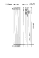
- FIG. 1 is a schematic diagram illustrating a modular computer system incorporating the invention
- FIG. 2 is a functional block diagram of the processor portion of the CPU module of FIG. 1;
- FIG. 3 is a schematic diagram illustrating the bus-module connection arrangement
- FIG. 4 is a block diagram of the polling elements incorporated into the modules of the FIG. 1 system
- FIG. 5 is a flow chart illustrating the polling sequence
- FIGS. 6A-6D illustrate a first specific embodiment of the module polling logic
- FIG. 7 is a diagram illustrating the interrelation of FIGS. 6A-6D;
- FIGS. 8A-8D are logic diagrams of a second specific embodiment of the polling logic.
- FIG. 9 is a diagram illustrating the interrelation of FIGS. 8A-8D.
- FIG. 1 illustrates a modular computer system incorporating the invention.
- the computer system includes a keyboard 10 for enabling operator input and control to the system, a CRT display 12 coupled to the keyboard 10 by means of interconnection cable 13, and a plurality of individual modules 15-18 arranged side by side.
- the left-most module 15 in the array is the CPU module, which is connected to the CRT display 12 by means of cable 19.
- the CPU module preferably incorporate an Intel type 80186 microcomputer and the block diagram of the processor board incorporated into module 15 is shown in FIG. 2.
- Modules 16-18 may comprise any one of a number of different modules, such as a graphics controller module, a dual floppy disk module, a hard disk module, a floppy/hard disk module or the like.
- a graphics controller module such as a graphics controller module, a dual floppy disk module, a hard disk module, a floppy/hard disk module or the like.
- the power supply connections have been omitted from all the Figs.
- Bus 11 comprises a plurality of internal conductors not visible in FIG. 3 and incorporates the usual bus address lines, bus data lines, and bus control lines.
- the preferred arrangement for mechanically and electrically interconnecting modules 15-18 is illustrated in commonly assigned copending U.S. patent application Ser. No. 493,089, filed May 9, 1983 for "Modular Housing For Computer System", now U.S. Pat. No. 4,501,460 issued Feb. 26, 1985 the disclosure of which is hereby incorporated by reference.
- the interconnection technique permits all modules to be readily interconnected both mechanically and electrically by means of mating male and female complementary plug and socket connections which are incorporated into the side walls (hidden from view in FIG.
- each module connected to the right of the CPU module 15 incorporates initial polling logic of the type illustrated in block diagram form in this Fig.
- a module identification unit 21 has an output coupled to the data bus 20.
- Module identification unit 21 is preferably a read only device, such as a plurality of hard wired connectors coupled to a corresponding plurality of tri-state buffers, or any other suitable type of read only device.
- Unit 21 is enabled to read out a unique module identification code, which is a multibit code in the preferred embodiment, in response to the appearance of an enable signal designated ID ENABLE, which is generated in the manner described below.
- Each module incorporating the logic shown in FIG. 4 also includes a base address register 23 having a data input which is also coupled to data bus 20, and an output coupled to one input of a comparator 24.
- the other input to comparator 24 comprises a multibit address placed on address bus 25 by the CPU within CPU module 15 in the manner described below.
- a buffer 26 is incorporated between the address bus 25 and the comparator 24.
- Control signals supplied to the polling logic in each module 16-18 include an input/output read signal designated XIORD, an input/output write signal designated XIOWR and a comparator disable signal designated XDMAEN.
- the XIORD signal is the standard I/O read signal employed in all read operations in the system, while the XIOWR control signal is the standard I/O write control signal used in the computer system.
- the XDMAEN control signal is used to disable comparator 24 during direct memory access (DMA) operations in the manner described below.
- Two input control signals are supplied to each module via the intermodule connection lines from the preceeding module immediately upstream: these two signals are RESET and XPIN.
- Two control signals are supplied by each module via the intermodule connection lines to the downstream or succeeding module. These signals are RESET and XPOUT.
- the XPIN and RESET control input signals for module 17 of FIG. 1 are the XPOUT and RESET signals from upstream module 16 of FIG. 1.
- the plus and minus symbols used in connection with some of the control signals illustrated in FIG. 4 indicate the active level.
- XPIN is active when in the relatively high state
- RESET is active when in the relatively low state.
- the polling logic in each downstream module includes a module select flipflop 28 and a write enable flipflop 29, each of which in the preferred embodiment are D type flipflops.
- the module select flipflop 28 has a data input D coupled to the XPIN control input terminal, a clock input CL coupled to the output of an inverting AND gate 31, a reset input R coupled to the output of an OR gate 32, and a Q output coupled as one input to NAND gate 31, NAND gate 32, and the input of an inverter 33.
- the two inputs to the OR gate 32 are the RESET signal and the XPIN signal from the upstream module.
- the output of inverter 33 comprises the XPOUT signal, which serves as the XPIN signal to the downstream module.
- Write enable flipflop 29 has a data input D also coupled to the XPIN control signal, a clock input CL coupled to the output of NAND gate 32, a reset input R coupled to the output of OR gate 32 and a Q output coupled as an input to NAND gate 31.
- the remaining inputs to NAND gate 31 are the XIOWR write control signal, and the output of comparator 24 designated MODSEL, which is active whenever the two addresses supplied to the comparator 24 match.
- the remaining inputs to NAND gate 32 comprise the XPIN signal, the MODSEL signal and the XIORD read control signal from the CPU.
- the XPIN control signal is also coupled via an inverter 34 as an enable signal to buffer 26.
- OR gate 32 is also coupled to the reset input R of register 23, and to an output terminal for supplying a RESET signal to the downstream module.
- the XDMAEN disable signal is coupled to the enable input of comparator 24 and serves to disable the comparator 24 during DMA operations, during which an erroneous MODSEL signal may be inadvertently generated.
- the RESET signal is automatically generated by the CPU and furnished to the module 16 immediately to the right of the CPU module 15.
- the appearance of the RESET signal causes the two flipflops 28 and 29 to be RESET and the register 23 to be reset to an all zero configuration, corresponding to the port 0 address.
- the reset signal is passed on to the succeeding downstream module 17, where the same reset transactions occur, and then to module 18. Consequently, upon power up all flipflops are reset and all base address registers are preset to address zero (port 0).
- the same reset action can be manually effected by operator manipulation of a machanical reset button, which is preferably mounted on the back panel of the CPU module 15.
- the polling operation proceeds as follows. With reference to FIGS. 4 and 5, the CPU pulls the XPIN control signal low momentarily (to ensure reset of at least the first downstream module 16 elements), and next raises the XPIN signal to the active state. Thereafter, the CPU issues a read port 0 command, which results in the appearance on address bus 25 of the port 0 address and the generation of an XIORD read control signal.
- the comparator 24 Since register 23 of the first downstream module 16 was previously preset to the port 0 address, the comparator 24 generates a MODSEL signal which qualifies NAND gate 32 (since XPIN, MODSEL FF, Q are all active) to pass the read command and generate an ID ENABLE signal, which results in the reading out of the module identification character from unit 21 onto data bus 20.
- This module identification character is received by the CPU and stored in a section of memory reserved for a table of module identification characters and bus address assignments.
- Generation of the ID enable signal clocks the write enable flipflop 29, which qualifies NAND gate 31 (since MODSEL and MODSEL FF Q are active) to pass the next IXIOWR write command and generate an IDADCK clock signal for register 23.
- an assigned base bus address is placed by the CPU on data bus 20, and this base address is thus clocked into register 23 when the IDADCK clock signal is generated.
- the IDADCK clock signal clocks flipflop 28 to the set state, which removes the modsel FF Q enabling signal from NAND gates 31 and 32, thereby disabling both gates until flipflop 28 is subsequently reset.
- the upper input to comparator 24 changes to a non-zero value with a result that the MODSEL comparator output signal goes inactive.
- flipflop 28 was reset, and the Q output of flipflop 28 inverted by inverter 33 caused the XPOUT signal to be at the inactive level, thereby preventing any downstream modules from participating in the polling sequence.
- the flipflop 28 is set, which changes the XPOUT signal to the active state, thereby permitting the next downstream module to become actively involved in the polling sequence.
- the I/O read/write polling sequence continues for each succeeding downstream module, with the CPU placing each successive module identification character in the CPU table and issuing a base bus address for that module.
- the CPU places each successive module identification character in the CPU table and issuing a base bus address for that module.
- an indicator 41 (FIG. 1) is provided on the front panel of each module 15-18.
- Indicators 41 are preferably driven by a signal generated by one of the two outputs of the module select flipflop 28.
- FIG. 6D One possible arrangement is illustrated in which the Q output from the flipflop is used to drive a light emitting diode 41 through an inverter. Other arrangements will occur to those skilled in the art.
- FIGS. 6A-D and 8A-D illustrate two different specific configurations of modules employing the automatic polling sequence described above. Other equivalent arrangements will occur to those skilled in the art.
- the system can be automatically reconfigured by entering the routine illustrated in FIG. 5, toggling the XPIN intermodule control line and performing the read port 0/write port 0 sequence.
- the same automatic polling sequence can be automatically conducted, and the same sequence may be initiated by manual operation of the reset switch.
- the system can be reconfigured at will.
- each register 23 is specifically described as being preset to the port 0 bus address at the beginning of the polling sequence, each register may be configured to preset to some other bus address, so long as the preset address is dedicated to the polling sequence. Therefore, the above descriptions and illustrations should not be construed as limiting the scope of the invention, which is defined by the appended claims.
Abstract
Description
Claims (8)
Priority Applications (3)
| Application Number | Priority Date | Filing Date | Title |
|---|---|---|---|
| US06/611,763 US4727475A (en) | 1984-05-18 | 1984-05-18 | Self-configuring modular computer system with automatic address initialization |
| AU42596/85A AU573344B2 (en) | 1984-05-18 | 1985-05-17 | Polling sequencer |
| CA000481810A CA1229420A (en) | 1984-05-18 | 1985-05-17 | Automatic polling sequence for modular computer system with expansion bus |
Applications Claiming Priority (1)
| Application Number | Priority Date | Filing Date | Title |
|---|---|---|---|
| US06/611,763 US4727475A (en) | 1984-05-18 | 1984-05-18 | Self-configuring modular computer system with automatic address initialization |
Publications (1)
| Publication Number | Publication Date |
|---|---|
| US4727475A true US4727475A (en) | 1988-02-23 |
Family
ID=24450322
Family Applications (1)
| Application Number | Title | Priority Date | Filing Date |
|---|---|---|---|
| US06/611,763 Expired - Lifetime US4727475A (en) | 1984-05-18 | 1984-05-18 | Self-configuring modular computer system with automatic address initialization |
Country Status (3)
| Country | Link |
|---|---|
| US (1) | US4727475A (en) |
| AU (1) | AU573344B2 (en) |
| CA (1) | CA1229420A (en) |
Cited By (96)
| Publication number | Priority date | Publication date | Assignee | Title |
|---|---|---|---|---|
| US4875158A (en) * | 1985-08-14 | 1989-10-17 | Apple Computer, Inc. | Method for requesting service by a device which generates a service request signal successively until it is serviced |
| US4888709A (en) * | 1987-03-27 | 1989-12-19 | Viscom Systems, Inc. | Electronic product information display system |
| US4896277A (en) * | 1988-05-03 | 1990-01-23 | Thermo King Corporation | Method of mapping refrigerated containers in a power line carrier based monitoring system |
| US4912627A (en) * | 1985-08-14 | 1990-03-27 | Apple Computer, Inc. | Method for storing a second number as a command address of a first peripheral device and a third number as a command address of a second peripheral device |
| US4918598A (en) * | 1985-08-14 | 1990-04-17 | Apple Computer, Inc. | Method for selectively activating and deactivating devices having same first address and different extended addresses |
| US4951248A (en) * | 1988-03-04 | 1990-08-21 | Sun Microsystems, Inc. | Self configuring memory system |
| US4962466A (en) * | 1987-03-27 | 1990-10-09 | Viscom Systems, Inc. | Electronic product information display system |
| US5019811A (en) * | 1984-10-15 | 1991-05-28 | Unigrafic Ag | Device for marking edges of shelves |
| US5029209A (en) * | 1990-06-13 | 1991-07-02 | The Boeing Company | Pseudorandom, iterative method and apparatus for automatically creating addresses |
| US5036479A (en) * | 1989-04-20 | 1991-07-30 | Trw Inc. | Modular automated avionics test system |
| US5051895A (en) * | 1987-09-17 | 1991-09-24 | Hewlett-Packard Company | Apparatus and method for tracking and identifying printed circuit assemblies |
| US5077684A (en) * | 1988-11-19 | 1991-12-31 | Nec Corporation | System for accurately informing each of adapters of its packaged location |
| WO1992004675A1 (en) * | 1990-08-30 | 1992-03-19 | Datacard Corporation | Dynamic address assignment of remote stations |
| US5122970A (en) * | 1988-06-17 | 1992-06-16 | Hewlett-Packard Company | Improved sensor |
| US5148389A (en) * | 1988-04-05 | 1992-09-15 | Convergent Technologies, Inc. | Modular expansion bus configuration |
| US5175822A (en) * | 1989-06-19 | 1992-12-29 | International Business Machines Corporation | Apparatus and method for assigning addresses to scsi supported peripheral devices |
| US5214771A (en) * | 1989-04-19 | 1993-05-25 | International Business Machines Corp. | System for loading same type adaptors with latest version control codes stored on adaptor memory by selecting the identified chip during initialization |
| US5218684A (en) * | 1987-09-04 | 1993-06-08 | Digital Equipment Corporation | Memory configuration system |
| US5239638A (en) * | 1988-12-30 | 1993-08-24 | Intel Corporation | Two strobed memory access |
| US5241627A (en) * | 1987-04-09 | 1993-08-31 | Tandem Computers Incorporated | Automatic processor module determination for multiprocessor systems for determining a value indicating the number of processors |
| US5257387A (en) * | 1988-09-09 | 1993-10-26 | Compaq Computer Corporation | Computer implemented method and apparatus for dynamic and automatic configuration of a computer system and circuit boards including computer resource allocation conflict resolution |
| US5261073A (en) * | 1989-05-05 | 1993-11-09 | Wang Laboratories, Inc. | Method and apparatus for providing memory system status signals |
| DE4216242A1 (en) * | 1992-05-16 | 1993-11-18 | Leuze Electronic Gmbh & Co | Identification method for sensors or actuators in bus system - having each sensor or actuator connected to bus via modular interface unit with switch |
| US5274780A (en) * | 1989-07-27 | 1993-12-28 | Mitsubishi Denki Kabushiki Kaisha | Bus controller for adjusting a bus master to a bus slave |
| US5317693A (en) * | 1991-04-04 | 1994-05-31 | Digital Equipment Corporation | Computer peripheral device network with peripheral address resetting capabilities |
| US5353413A (en) * | 1992-03-19 | 1994-10-04 | Aeg Transportation Systems, Inc. | Method and apparatus for christening a trainline monitor system |
| US5357621A (en) * | 1990-09-04 | 1994-10-18 | Hewlett-Packard Company | Serial architecture for memory module control |
| US5367647A (en) * | 1991-08-19 | 1994-11-22 | Sequent Computer Systems, Inc. | Apparatus and method for achieving improved SCSI bus control capacity |
| US5373288A (en) * | 1992-10-23 | 1994-12-13 | At&T Corp. | Initializing terminals in a signal distribution system |
| US5388224A (en) * | 1992-04-24 | 1995-02-07 | Digital Equipment Corporation | Processor identification mechanism for a multiprocessor system |
| US5408229A (en) * | 1992-03-02 | 1995-04-18 | Mitsubishi Denki Kabushiki Kaisha | Programmable controller which allows for removal of the I/O modules during an on-line mode |
| US5416777A (en) * | 1991-04-10 | 1995-05-16 | California Institute Of Technology | High speed polling protocol for multiple node network |
| US5420987A (en) * | 1993-07-19 | 1995-05-30 | 3 Com Corporation | Method and apparatus for configuring a selected adapter unit on a common bus in the presence of other adapter units |
| US5437019A (en) * | 1990-12-17 | 1995-07-25 | Hewlett-Packard Company | Addressing method and apparatus for a computer system |
| US5452424A (en) * | 1990-08-31 | 1995-09-19 | Ncr Corporation | Work station and method for serially providing configuration data to functional units contained therein |
| DE4429433C1 (en) * | 1994-08-19 | 1995-10-26 | Siemens Ag | Address association method for modular stored program controller |
| DE4421344A1 (en) * | 1994-06-17 | 1995-12-21 | Hartmut B Dr Brinkhus | Computer add-on expansion card with software-driven configuration |
| US5517617A (en) * | 1994-06-29 | 1996-05-14 | Digital Equipment Corporation | Automatic assignment of addresses in a computer communications network |
| US5535336A (en) * | 1990-09-19 | 1996-07-09 | Intel Corporation | Apparatus and method for enabling a network interface to dynamically assign an address to a connected computer and to establish a virtual circuit with another network interface |
| US5535368A (en) * | 1991-11-12 | 1996-07-09 | International Business Machines Corporation | Automatically-configuring memory subsystem |
| US5564025A (en) * | 1992-08-10 | 1996-10-08 | U.S. Philips Corporation | Apparatus for arbitrating requests for access from slave units by associating the requests with master units and determining the relative pendency thereof in a radio base station transceiver |
| US5564110A (en) * | 1987-03-10 | 1996-10-08 | Canon Kabushiki Kaisha | Printer interface apparatus with plug-in unit authorized for reception of data upon type verification |
| US5564033A (en) * | 1993-06-29 | 1996-10-08 | Hitachi, Ltd. | Disk array system using detachable memory medium |
| US5594874A (en) * | 1993-09-30 | 1997-01-14 | Cirrus Logic, Inc. | Automatic bus setting, sensing and switching interface unit |
| US5613158A (en) * | 1994-05-25 | 1997-03-18 | Tandem Computers, Inc. | System for specifying addresses by creating a multi-bit ranked ordered anchor pattern and creating next address by shifting in the direction of the superior position |
| US5630167A (en) * | 1988-03-18 | 1997-05-13 | Canon Kabushiki Kaisha | Electronic apparatus having a plurality of connectors each connecting one of a plurality of kinds of cards |
| US5636342A (en) * | 1995-02-17 | 1997-06-03 | Dell Usa, L.P. | Systems and method for assigning unique addresses to agents on a system management bus |
| US5655148A (en) * | 1994-05-27 | 1997-08-05 | Microsoft Corporation | Method for automatically configuring devices including a network adapter without manual intervention and without prior configuration information |
| US5687342A (en) * | 1991-09-18 | 1997-11-11 | Ncr Corporation | Memory range detector and translator |
| US5727184A (en) * | 1994-06-27 | 1998-03-10 | Cirrus Logic, Inc. | Method and apparatus for interfacing between peripherals of multiple formats and a single system bus |
| US5727169A (en) * | 1990-06-12 | 1998-03-10 | Sgs-Thomson Microelectronics, S.A. | Electronically configurable connection device |
| US5734659A (en) * | 1984-06-01 | 1998-03-31 | Digital Equipment Corporation | Computer network having a virtual circuit message carrying a plurality of session messages |
| US5748980A (en) * | 1994-05-27 | 1998-05-05 | Microsoft Corporation | System for configuring a computer system |
| US5787306A (en) * | 1994-05-18 | 1998-07-28 | National Semiconductor Corporation | Automatic assignment of I/O addresses in a computer system |
| US5787246A (en) * | 1994-05-27 | 1998-07-28 | Microsoft Corporation | System for configuring devices for a computer system |
| US5794014A (en) * | 1994-06-27 | 1998-08-11 | Cirrus Logic, Inc. | Method and apparatus for interfacing between peripherals of multiple formats and a single system bus |
| WO1998037977A1 (en) * | 1997-02-27 | 1998-09-03 | Patchen, Inc. | An agricultural implement having multiple agents for mapping fields |
| US5818350A (en) * | 1995-04-11 | 1998-10-06 | Lexar Microsystems Inc. | High performance method of and system for selecting one of a plurality of IC chip while requiring minimal select lines |
| US5828899A (en) * | 1996-01-04 | 1998-10-27 | Compaq Computer Corporation | System for peripheral devices recursively generating unique addresses based on the number of devices connected dependent upon the relative position to the port |
| US5833375A (en) * | 1996-09-20 | 1998-11-10 | Varis Corporation | System and method for interfacing a raster printer controller with a plurality of print engines |
| US5841365A (en) * | 1993-09-22 | 1998-11-24 | Seattle Silicon Corporation | Method and apparatus for communicating with a product label |
| US5938742A (en) * | 1995-08-18 | 1999-08-17 | General Magic, Inc. | Method for configuring an intelligent low power serial bus |
| US5987548A (en) * | 1997-07-07 | 1999-11-16 | International Business Machines Corporation | Method and apparatus for determining system identification number system using system data bus and pull-up resistors in combination with a sensing circuitry |
| US6038195A (en) * | 1990-04-18 | 2000-03-14 | Rambus Inc. | Synchronous memory device having a delay time register and method of operating same |
| US6061739A (en) * | 1997-11-26 | 2000-05-09 | International Business Machines Corp. | Network address assignment using physical address resolution protocols |
| DE19857255C1 (en) * | 1998-12-11 | 2000-08-03 | Hartmut B Brinkhus | Self-configuring modular electronic system, especially computer system |
| US6119185A (en) * | 1997-11-25 | 2000-09-12 | Ncr Corporation | Computer system configuration apparatus and method that performs pre-assignment conflict analysis |
| US6202138B1 (en) | 1995-07-31 | 2001-03-13 | Lexar Media, Inc | Increasing the memory performance of flash memory devices by writing sectors simultaneously to multiple flash memory devices |
| EP1100018A2 (en) * | 1999-11-11 | 2001-05-16 | Sankyo Seiki Mfg. Co. Ltd. | USB-Interface Equipped Device |
| US6240496B1 (en) * | 1989-11-24 | 2001-05-29 | Hyundai Electronics America | Architecture and configuring method for a computer expansion board |
| US6256034B1 (en) | 1986-06-27 | 2001-07-03 | Sture Olsson | Device for marking edges of shelves |
| US6272446B1 (en) | 1995-12-22 | 2001-08-07 | Bruel & Kjaer Sound & Vibration Measurement A/S | System and a method for measuring a continuous signal |
| US6321374B1 (en) | 1997-11-07 | 2001-11-20 | International Business Machines Corporation | Application-independent generator to generate a database transaction manager in heterogeneous information systems |
| US6374337B1 (en) | 1998-11-17 | 2002-04-16 | Lexar Media, Inc. | Data pipelining method and apparatus for memory control circuit |
| US6411546B1 (en) | 1997-03-31 | 2002-06-25 | Lexar Media, Inc. | Nonvolatile memory using flexible erasing methods and method and system for using same |
| US20020194468A1 (en) * | 2001-06-18 | 2002-12-19 | Betts-Lacroix Jonathan | Modular computing system |
| US20030023753A1 (en) * | 2001-07-26 | 2003-01-30 | Rychlicki Victor John | Method of addressing networked devices |
| DE10142810A1 (en) * | 2001-08-31 | 2003-04-03 | Audi Ag | Automated bus configuration |
| US6564308B2 (en) | 1989-05-05 | 2003-05-13 | Samsung Electronics Co. Ltd. | Multiple mode memory module |
| US20030231168A1 (en) * | 2002-06-18 | 2003-12-18 | Jory Bell | Component for use as a portable computing device and pointing device in a modular computing system |
| US6711673B1 (en) * | 2000-01-03 | 2004-03-23 | Advanced Micro Devices, Inc. | Using a model specific register as a base I/O address register for embedded I/O registers in a processor |
| US6728851B1 (en) | 1995-07-31 | 2004-04-27 | Lexar Media, Inc. | Increasing the memory performance of flash memory devices by writing sectors simultaneously to multiple flash memory devices |
| US6757800B1 (en) | 1995-07-31 | 2004-06-29 | Lexar Media, Inc. | Increasing the memory performance of flash memory devices by writing sectors simultaneously to multiple flash memory devices |
| US6763454B2 (en) | 1994-05-27 | 2004-07-13 | Microsoft Corp. | System for allocating resources in a computer system |
| US20040186935A1 (en) * | 2003-03-18 | 2004-09-23 | Jory Bell | Component for use as a portable computing device and pointing device |
| US6801979B1 (en) | 1995-07-31 | 2004-10-05 | Lexar Media, Inc. | Method and apparatus for memory control circuit |
| US20040215841A1 (en) * | 2003-04-23 | 2004-10-28 | Tsutomu Yamada | Modular computer system and I/O module |
| US20050024213A1 (en) * | 2003-08-01 | 2005-02-03 | David Franzen | Sensor and method of detecting the condition of a turf grass |
| US20050172109A1 (en) * | 2001-06-01 | 2005-08-04 | Microchip Technology Incorporated | Register pointer trap |
| US20050185364A1 (en) * | 2004-01-05 | 2005-08-25 | Jory Bell | Docking station for mobile computing device |
| US20070088879A1 (en) * | 2005-10-07 | 2007-04-19 | Via Technologies, Inc. | Method for initializing bus device |
| US20070142946A1 (en) * | 2005-12-17 | 2007-06-21 | Dr. Johannes Heidenhain Gmbh | Method for the start-up of numerical controls of machine tools or production machinery and numerical control for machine tools or production machinery |
| US20110022747A1 (en) * | 2002-06-18 | 2011-01-27 | Betts-Lacroix Jonathan | Modular computing system |
| US20150026077A1 (en) * | 2013-07-18 | 2015-01-22 | Netapp, Inc. | Centralized Method for Customer Assistance and System Verification |
| US20150026076A1 (en) * | 2013-07-18 | 2015-01-22 | Netapp, Inc. | System and Method for Providing Customer Guidance in Deploying a Computing System |
| US9126066B2 (en) | 2010-04-08 | 2015-09-08 | Fire Research Corp. | Smart connector for integration of a foam proportioning system with fire extinguishing equipment |
Citations (6)
| Publication number | Priority date | Publication date | Assignee | Title |
|---|---|---|---|---|
| US4025903A (en) * | 1973-09-10 | 1977-05-24 | Computer Automation, Inc. | Automatic modular memory address allocation system |
| US4281392A (en) * | 1979-05-01 | 1981-07-28 | Allen-Bradley Company | Memory circuit for programmable machines |
| US4360870A (en) * | 1980-07-30 | 1982-11-23 | International Business Machines Corporation | Programmable I/O device identification |
| US4468729A (en) * | 1981-06-29 | 1984-08-28 | Sperry Corporation | Automatic memory module address assignment system for available memory modules |
| US4562535A (en) * | 1982-04-05 | 1985-12-31 | Texas Instruments Incorporated | Self-configuring digital processor system with global system |
| US4622633A (en) * | 1983-12-06 | 1986-11-11 | Tri Sigma Corporation | Object building method for self configuring computer network |
-
1984
- 1984-05-18 US US06/611,763 patent/US4727475A/en not_active Expired - Lifetime
-
1985
- 1985-05-17 CA CA000481810A patent/CA1229420A/en not_active Expired
- 1985-05-17 AU AU42596/85A patent/AU573344B2/en not_active Ceased
Patent Citations (6)
| Publication number | Priority date | Publication date | Assignee | Title |
|---|---|---|---|---|
| US4025903A (en) * | 1973-09-10 | 1977-05-24 | Computer Automation, Inc. | Automatic modular memory address allocation system |
| US4281392A (en) * | 1979-05-01 | 1981-07-28 | Allen-Bradley Company | Memory circuit for programmable machines |
| US4360870A (en) * | 1980-07-30 | 1982-11-23 | International Business Machines Corporation | Programmable I/O device identification |
| US4468729A (en) * | 1981-06-29 | 1984-08-28 | Sperry Corporation | Automatic memory module address assignment system for available memory modules |
| US4562535A (en) * | 1982-04-05 | 1985-12-31 | Texas Instruments Incorporated | Self-configuring digital processor system with global system |
| US4622633A (en) * | 1983-12-06 | 1986-11-11 | Tri Sigma Corporation | Object building method for self configuring computer network |
Cited By (142)
| Publication number | Priority date | Publication date | Assignee | Title |
|---|---|---|---|---|
| US5734659A (en) * | 1984-06-01 | 1998-03-31 | Digital Equipment Corporation | Computer network having a virtual circuit message carrying a plurality of session messages |
| US5313569A (en) * | 1984-10-15 | 1994-05-17 | Unigrafic Ag | Device for marking edges of shelves |
| US5019811A (en) * | 1984-10-15 | 1991-05-28 | Unigrafic Ag | Device for marking edges of shelves |
| US4912627A (en) * | 1985-08-14 | 1990-03-27 | Apple Computer, Inc. | Method for storing a second number as a command address of a first peripheral device and a third number as a command address of a second peripheral device |
| US4918598A (en) * | 1985-08-14 | 1990-04-17 | Apple Computer, Inc. | Method for selectively activating and deactivating devices having same first address and different extended addresses |
| US4875158A (en) * | 1985-08-14 | 1989-10-17 | Apple Computer, Inc. | Method for requesting service by a device which generates a service request signal successively until it is serviced |
| US6256034B1 (en) | 1986-06-27 | 2001-07-03 | Sture Olsson | Device for marking edges of shelves |
| US5564110A (en) * | 1987-03-10 | 1996-10-08 | Canon Kabushiki Kaisha | Printer interface apparatus with plug-in unit authorized for reception of data upon type verification |
| US4962466A (en) * | 1987-03-27 | 1990-10-09 | Viscom Systems, Inc. | Electronic product information display system |
| US4888709A (en) * | 1987-03-27 | 1989-12-19 | Viscom Systems, Inc. | Electronic product information display system |
| US5241627A (en) * | 1987-04-09 | 1993-08-31 | Tandem Computers Incorporated | Automatic processor module determination for multiprocessor systems for determining a value indicating the number of processors |
| US5218684A (en) * | 1987-09-04 | 1993-06-08 | Digital Equipment Corporation | Memory configuration system |
| US5051895A (en) * | 1987-09-17 | 1991-09-24 | Hewlett-Packard Company | Apparatus and method for tracking and identifying printed circuit assemblies |
| US4951248A (en) * | 1988-03-04 | 1990-08-21 | Sun Microsystems, Inc. | Self configuring memory system |
| US5630167A (en) * | 1988-03-18 | 1997-05-13 | Canon Kabushiki Kaisha | Electronic apparatus having a plurality of connectors each connecting one of a plurality of kinds of cards |
| US5148389A (en) * | 1988-04-05 | 1992-09-15 | Convergent Technologies, Inc. | Modular expansion bus configuration |
| US4896277A (en) * | 1988-05-03 | 1990-01-23 | Thermo King Corporation | Method of mapping refrigerated containers in a power line carrier based monitoring system |
| US5122970A (en) * | 1988-06-17 | 1992-06-16 | Hewlett-Packard Company | Improved sensor |
| US5257387A (en) * | 1988-09-09 | 1993-10-26 | Compaq Computer Corporation | Computer implemented method and apparatus for dynamic and automatic configuration of a computer system and circuit boards including computer resource allocation conflict resolution |
| US5077684A (en) * | 1988-11-19 | 1991-12-31 | Nec Corporation | System for accurately informing each of adapters of its packaged location |
| US5239638A (en) * | 1988-12-30 | 1993-08-24 | Intel Corporation | Two strobed memory access |
| US5214771A (en) * | 1989-04-19 | 1993-05-25 | International Business Machines Corp. | System for loading same type adaptors with latest version control codes stored on adaptor memory by selecting the identified chip during initialization |
| US5036479A (en) * | 1989-04-20 | 1991-07-30 | Trw Inc. | Modular automated avionics test system |
| US5261073A (en) * | 1989-05-05 | 1993-11-09 | Wang Laboratories, Inc. | Method and apparatus for providing memory system status signals |
| US6499093B2 (en) * | 1989-05-05 | 2002-12-24 | Samsung Electronics Co., Ltd. | Multiple mode memory module |
| US6021477A (en) * | 1989-05-05 | 2000-02-01 | Samsung Electronics Co., Ltd | Multiple mode memory module |
| US6564308B2 (en) | 1989-05-05 | 2003-05-13 | Samsung Electronics Co. Ltd. | Multiple mode memory module |
| US5175822A (en) * | 1989-06-19 | 1992-12-29 | International Business Machines Corporation | Apparatus and method for assigning addresses to scsi supported peripheral devices |
| US5274780A (en) * | 1989-07-27 | 1993-12-28 | Mitsubishi Denki Kabushiki Kaisha | Bus controller for adjusting a bus master to a bus slave |
| US6711658B2 (en) | 1989-11-24 | 2004-03-23 | Hyundai Electronics America | Architecture and configuring method for a computer expansion board |
| US6240496B1 (en) * | 1989-11-24 | 2001-05-29 | Hyundai Electronics America | Architecture and configuring method for a computer expansion board |
| US6128696A (en) * | 1990-04-18 | 2000-10-03 | Rambus Inc. | Synchronous memory device utilizing request protocol and method of operation of same |
| US20050141332A1 (en) * | 1990-04-18 | 2005-06-30 | Rambus Inc. | Semiconductor device including a register to store a value that is representative of device type information |
| US6044426A (en) * | 1990-04-18 | 2000-03-28 | Rambus Inc. | Memory system having memory devices each including a programmable internal register |
| US6067592A (en) * | 1990-04-18 | 2000-05-23 | Rambus Inc. | System having a synchronous memory device |
| US6070222A (en) * | 1990-04-18 | 2000-05-30 | Rambus Inc. | Synchronous memory device having identification register |
| US6085284A (en) * | 1990-04-18 | 2000-07-04 | Rambus Inc. | Method of operating a memory device having a variable data output length and an identification register |
| US20040114454A1 (en) * | 1990-04-18 | 2004-06-17 | Rambus Inc. | Memory device and method for operating same |
| US6185644B1 (en) | 1990-04-18 | 2001-02-06 | Rambus Inc. | Memory system including a plurality of memory devices and a transceiver device |
| US6415339B1 (en) | 1990-04-18 | 2002-07-02 | Rambus Inc. | Memory device having a plurality of programmable internal registers and a delay time register |
| US6038195A (en) * | 1990-04-18 | 2000-03-14 | Rambus Inc. | Synchronous memory device having a delay time register and method of operating same |
| US5727169A (en) * | 1990-06-12 | 1998-03-10 | Sgs-Thomson Microelectronics, S.A. | Electronically configurable connection device |
| US5029209A (en) * | 1990-06-13 | 1991-07-02 | The Boeing Company | Pseudorandom, iterative method and apparatus for automatically creating addresses |
| US5204669A (en) * | 1990-08-30 | 1993-04-20 | Datacard Corporation | Automatic station identification where function modules automatically initialize |
| WO1992004675A1 (en) * | 1990-08-30 | 1992-03-19 | Datacard Corporation | Dynamic address assignment of remote stations |
| US5452424A (en) * | 1990-08-31 | 1995-09-19 | Ncr Corporation | Work station and method for serially providing configuration data to functional units contained therein |
| US5357621A (en) * | 1990-09-04 | 1994-10-18 | Hewlett-Packard Company | Serial architecture for memory module control |
| US5535336A (en) * | 1990-09-19 | 1996-07-09 | Intel Corporation | Apparatus and method for enabling a network interface to dynamically assign an address to a connected computer and to establish a virtual circuit with another network interface |
| US5437019A (en) * | 1990-12-17 | 1995-07-25 | Hewlett-Packard Company | Addressing method and apparatus for a computer system |
| US5317693A (en) * | 1991-04-04 | 1994-05-31 | Digital Equipment Corporation | Computer peripheral device network with peripheral address resetting capabilities |
| US5416777A (en) * | 1991-04-10 | 1995-05-16 | California Institute Of Technology | High speed polling protocol for multiple node network |
| US5367647A (en) * | 1991-08-19 | 1994-11-22 | Sequent Computer Systems, Inc. | Apparatus and method for achieving improved SCSI bus control capacity |
| US5687342A (en) * | 1991-09-18 | 1997-11-11 | Ncr Corporation | Memory range detector and translator |
| US5535368A (en) * | 1991-11-12 | 1996-07-09 | International Business Machines Corporation | Automatically-configuring memory subsystem |
| US5408229A (en) * | 1992-03-02 | 1995-04-18 | Mitsubishi Denki Kabushiki Kaisha | Programmable controller which allows for removal of the I/O modules during an on-line mode |
| US5353413A (en) * | 1992-03-19 | 1994-10-04 | Aeg Transportation Systems, Inc. | Method and apparatus for christening a trainline monitor system |
| US5388224A (en) * | 1992-04-24 | 1995-02-07 | Digital Equipment Corporation | Processor identification mechanism for a multiprocessor system |
| DE4216242A1 (en) * | 1992-05-16 | 1993-11-18 | Leuze Electronic Gmbh & Co | Identification method for sensors or actuators in bus system - having each sensor or actuator connected to bus via modular interface unit with switch |
| US5564025A (en) * | 1992-08-10 | 1996-10-08 | U.S. Philips Corporation | Apparatus for arbitrating requests for access from slave units by associating the requests with master units and determining the relative pendency thereof in a radio base station transceiver |
| US5373288A (en) * | 1992-10-23 | 1994-12-13 | At&T Corp. | Initializing terminals in a signal distribution system |
| US5559503A (en) * | 1992-10-23 | 1996-09-24 | Lucent Technologies Inc. | Communications device for initializing terminals in a signal distribution system |
| US5564033A (en) * | 1993-06-29 | 1996-10-08 | Hitachi, Ltd. | Disk array system using detachable memory medium |
| US5420987A (en) * | 1993-07-19 | 1995-05-30 | 3 Com Corporation | Method and apparatus for configuring a selected adapter unit on a common bus in the presence of other adapter units |
| US5841365A (en) * | 1993-09-22 | 1998-11-24 | Seattle Silicon Corporation | Method and apparatus for communicating with a product label |
| US5594874A (en) * | 1993-09-30 | 1997-01-14 | Cirrus Logic, Inc. | Automatic bus setting, sensing and switching interface unit |
| US5787306A (en) * | 1994-05-18 | 1998-07-28 | National Semiconductor Corporation | Automatic assignment of I/O addresses in a computer system |
| USRE37613E1 (en) * | 1994-05-25 | 2002-03-26 | Compaq Cupertino Corporation | System for specifying addresses by creating a multi-bit ranked ordered anchor pattern and creating next address by shifting in the direction of the superior position |
| US5613158A (en) * | 1994-05-25 | 1997-03-18 | Tandem Computers, Inc. | System for specifying addresses by creating a multi-bit ranked ordered anchor pattern and creating next address by shifting in the direction of the superior position |
| US5787246A (en) * | 1994-05-27 | 1998-07-28 | Microsoft Corporation | System for configuring devices for a computer system |
| US5748980A (en) * | 1994-05-27 | 1998-05-05 | Microsoft Corporation | System for configuring a computer system |
| US5809329A (en) * | 1994-05-27 | 1998-09-15 | Microsoft Corporation | System for managing the configuration of a computer system |
| US6763454B2 (en) | 1994-05-27 | 2004-07-13 | Microsoft Corp. | System for allocating resources in a computer system |
| US6003097A (en) * | 1994-05-27 | 1999-12-14 | Microsoft Corporation | System for automatically configuring a network adapter without manual intervention by using a registry data structure maintained within a computer system memory |
| US5819107A (en) * | 1994-05-27 | 1998-10-06 | Microsoft Corporation | Method for managing the assignment of device drivers in a computer system |
| US7308511B2 (en) | 1994-05-27 | 2007-12-11 | Microsoft Corporation | System for allocating resources in a computer system |
| US20040205258A1 (en) * | 1994-05-27 | 2004-10-14 | Microsoft Corp. | System for allocating resources in a computer system |
| US5793979A (en) * | 1994-05-27 | 1998-08-11 | Microsoft Corporation | System for allocating the resources of a computer system |
| US6336152B1 (en) | 1994-05-27 | 2002-01-01 | Microsoft Corporation | Method for automatically configuring devices including a network adapter without manual intervention and without prior configuration information |
| US5655148A (en) * | 1994-05-27 | 1997-08-05 | Microsoft Corporation | Method for automatically configuring devices including a network adapter without manual intervention and without prior configuration information |
| DE4421344A1 (en) * | 1994-06-17 | 1995-12-21 | Hartmut B Dr Brinkhus | Computer add-on expansion card with software-driven configuration |
| US5905885A (en) * | 1994-06-27 | 1999-05-18 | Cirrus Logic, Inc. | Method and apparatus for interfacing between peripherals of multiple formats and a single system bus |
| US5794014A (en) * | 1994-06-27 | 1998-08-11 | Cirrus Logic, Inc. | Method and apparatus for interfacing between peripherals of multiple formats and a single system bus |
| US5727184A (en) * | 1994-06-27 | 1998-03-10 | Cirrus Logic, Inc. | Method and apparatus for interfacing between peripherals of multiple formats and a single system bus |
| US5517617A (en) * | 1994-06-29 | 1996-05-14 | Digital Equipment Corporation | Automatic assignment of addresses in a computer communications network |
| US5740379A (en) * | 1994-08-19 | 1998-04-14 | Siemens Aktiengesellschaft | Method for generating unique addresses for electrical devices from input bit patterns being verifiable for admissibility |
| DE4429433C1 (en) * | 1994-08-19 | 1995-10-26 | Siemens Ag | Address association method for modular stored program controller |
| US5636342A (en) * | 1995-02-17 | 1997-06-03 | Dell Usa, L.P. | Systems and method for assigning unique addresses to agents on a system management bus |
| US6009479A (en) * | 1995-02-17 | 1999-12-28 | Dell Usa, L.P. | System and method for assigning unique addresses to agents on a system management bus |
| US5818350A (en) * | 1995-04-11 | 1998-10-06 | Lexar Microsystems Inc. | High performance method of and system for selecting one of a plurality of IC chip while requiring minimal select lines |
| US6202138B1 (en) | 1995-07-31 | 2001-03-13 | Lexar Media, Inc | Increasing the memory performance of flash memory devices by writing sectors simultaneously to multiple flash memory devices |
| US6801979B1 (en) | 1995-07-31 | 2004-10-05 | Lexar Media, Inc. | Method and apparatus for memory control circuit |
| US6728851B1 (en) | 1995-07-31 | 2004-04-27 | Lexar Media, Inc. | Increasing the memory performance of flash memory devices by writing sectors simultaneously to multiple flash memory devices |
| US6397314B1 (en) | 1995-07-31 | 2002-05-28 | Lexar Media, Inc. | Increasing the memory performance of flash memory devices by writing sectors simultaneously to multiple flash memory devices |
| US6757800B1 (en) | 1995-07-31 | 2004-06-29 | Lexar Media, Inc. | Increasing the memory performance of flash memory devices by writing sectors simultaneously to multiple flash memory devices |
| US5938742A (en) * | 1995-08-18 | 1999-08-17 | General Magic, Inc. | Method for configuring an intelligent low power serial bus |
| US6272446B1 (en) | 1995-12-22 | 2001-08-07 | Bruel & Kjaer Sound & Vibration Measurement A/S | System and a method for measuring a continuous signal |
| US5828899A (en) * | 1996-01-04 | 1998-10-27 | Compaq Computer Corporation | System for peripheral devices recursively generating unique addresses based on the number of devices connected dependent upon the relative position to the port |
| US5833375A (en) * | 1996-09-20 | 1998-11-10 | Varis Corporation | System and method for interfacing a raster printer controller with a plurality of print engines |
| WO1998037977A1 (en) * | 1997-02-27 | 1998-09-03 | Patchen, Inc. | An agricultural implement having multiple agents for mapping fields |
| US5809440A (en) * | 1997-02-27 | 1998-09-15 | Patchen, Inc. | Agricultural implement having multiple agents for mapping fields |
| US6587382B1 (en) | 1997-03-31 | 2003-07-01 | Lexar Media, Inc. | Nonvolatile memory using flexible erasing methods and method and system for using same |
| US6411546B1 (en) | 1997-03-31 | 2002-06-25 | Lexar Media, Inc. | Nonvolatile memory using flexible erasing methods and method and system for using same |
| US5987548A (en) * | 1997-07-07 | 1999-11-16 | International Business Machines Corporation | Method and apparatus for determining system identification number system using system data bus and pull-up resistors in combination with a sensing circuitry |
| US6321374B1 (en) | 1997-11-07 | 2001-11-20 | International Business Machines Corporation | Application-independent generator to generate a database transaction manager in heterogeneous information systems |
| US6119185A (en) * | 1997-11-25 | 2000-09-12 | Ncr Corporation | Computer system configuration apparatus and method that performs pre-assignment conflict analysis |
| US6061739A (en) * | 1997-11-26 | 2000-05-09 | International Business Machines Corp. | Network address assignment using physical address resolution protocols |
| US6374337B1 (en) | 1998-11-17 | 2002-04-16 | Lexar Media, Inc. | Data pipelining method and apparatus for memory control circuit |
| US6516377B1 (en) * | 1998-12-11 | 2003-02-04 | Hartmut B. Brinkhus | Self-configuring modular electronic system |
| DE19857255C1 (en) * | 1998-12-11 | 2000-08-03 | Hartmut B Brinkhus | Self-configuring modular electronic system, especially computer system |
| EP1100018A2 (en) * | 1999-11-11 | 2001-05-16 | Sankyo Seiki Mfg. Co. Ltd. | USB-Interface Equipped Device |
| EP1100018A3 (en) * | 1999-11-11 | 2001-10-04 | Sankyo Seiki Mfg. Co. Ltd. | USB-Interface Equipped Device |
| US6711673B1 (en) * | 2000-01-03 | 2004-03-23 | Advanced Micro Devices, Inc. | Using a model specific register as a base I/O address register for embedded I/O registers in a processor |
| US7966480B2 (en) * | 2001-06-01 | 2011-06-21 | Microchip Technology Incorporated | Register pointer trap to prevent errors due to an invalid pointer value in a register |
| US20050172109A1 (en) * | 2001-06-01 | 2005-08-04 | Microchip Technology Incorporated | Register pointer trap |
| US20020194468A1 (en) * | 2001-06-18 | 2002-12-19 | Betts-Lacroix Jonathan | Modular computing system |
| US7159038B2 (en) | 2001-07-26 | 2007-01-02 | Victor John Rychlicki | Method of addressing networked devices |
| US20030023753A1 (en) * | 2001-07-26 | 2003-01-30 | Rychlicki Victor John | Method of addressing networked devices |
| DE10142810A1 (en) * | 2001-08-31 | 2003-04-03 | Audi Ag | Automated bus configuration |
| US20030231168A1 (en) * | 2002-06-18 | 2003-12-18 | Jory Bell | Component for use as a portable computing device and pointing device in a modular computing system |
| US20110022747A1 (en) * | 2002-06-18 | 2011-01-27 | Betts-Lacroix Jonathan | Modular computing system |
| US20040186935A1 (en) * | 2003-03-18 | 2004-09-23 | Jory Bell | Component for use as a portable computing device and pointing device |
| US7054965B2 (en) | 2003-03-18 | 2006-05-30 | Oqo Incorporated | Component for use as a portable computing device and pointing device |
| US20070266184A1 (en) * | 2003-04-23 | 2007-11-15 | Tsutomu Yamada | Modular computer system and i/o module |
| US7941567B2 (en) | 2003-04-23 | 2011-05-10 | Hitachi, Ltd. | Modular computer system and I/O module |
| US7272665B2 (en) * | 2003-04-23 | 2007-09-18 | Hitachi, Ltd. | Modular computer system and I/O module |
| US20040215841A1 (en) * | 2003-04-23 | 2004-10-28 | Tsutomu Yamada | Modular computer system and I/O module |
| US8482736B2 (en) | 2003-08-01 | 2013-07-09 | David Franzen | Sensor and method of detecting the condition of a turf grass |
| US20060151680A1 (en) * | 2003-08-01 | 2006-07-13 | David Franzen | Sensor and method of detecting the condition of a turf grass |
| US20110235043A1 (en) * | 2003-08-01 | 2011-09-29 | Li-Cor, Inc. | Sensor and method of detecting the condition of a turf grass |
| US7362439B2 (en) | 2003-08-01 | 2008-04-22 | Li-Cor, Inc. | Method of detecting the condition of a turf grass |
| US20080316491A1 (en) * | 2003-08-01 | 2008-12-25 | Li-Cor, Inc. | Sensor and method of detecting the condition of a turf grass |
| US20050024213A1 (en) * | 2003-08-01 | 2005-02-03 | David Franzen | Sensor and method of detecting the condition of a turf grass |
| US7911616B2 (en) | 2003-08-01 | 2011-03-22 | Li-Cor, Inc. | Sensor and method of detecting the condition of a turf grass |
| US7929141B2 (en) | 2003-08-01 | 2011-04-19 | Li-Cor, Inc. | Sensor and method of detecting the condition of a turf grass |
| US20050185364A1 (en) * | 2004-01-05 | 2005-08-25 | Jory Bell | Docking station for mobile computing device |
| US7900028B2 (en) * | 2005-10-07 | 2011-03-01 | Via Technologies, Inc. | Method for initializing bus device |
| US20070088879A1 (en) * | 2005-10-07 | 2007-04-19 | Via Technologies, Inc. | Method for initializing bus device |
| US8032738B2 (en) * | 2005-12-17 | 2011-10-04 | Dr. Johannes Heidenhain Gmbh | Method for the start-up of numerical controls of machine tools or production machinery and numerical control for machine tools or production machinery |
| US20070142946A1 (en) * | 2005-12-17 | 2007-06-21 | Dr. Johannes Heidenhain Gmbh | Method for the start-up of numerical controls of machine tools or production machinery and numerical control for machine tools or production machinery |
| US9126066B2 (en) | 2010-04-08 | 2015-09-08 | Fire Research Corp. | Smart connector for integration of a foam proportioning system with fire extinguishing equipment |
| US20150026077A1 (en) * | 2013-07-18 | 2015-01-22 | Netapp, Inc. | Centralized Method for Customer Assistance and System Verification |
| US20150026076A1 (en) * | 2013-07-18 | 2015-01-22 | Netapp, Inc. | System and Method for Providing Customer Guidance in Deploying a Computing System |
Also Published As
| Publication number | Publication date |
|---|---|
| CA1229420A (en) | 1987-11-17 |
| AU4259685A (en) | 1985-11-21 |
| AU573344B2 (en) | 1988-06-02 |
Similar Documents
| Publication | Publication Date | Title |
|---|---|---|
| US4727475A (en) | Self-configuring modular computer system with automatic address initialization | |
| US4964038A (en) | Data processing system having automatic address allocation arrangements for addressing interface cards | |
| EP0044949B1 (en) | Dynamic peripheral device address assignment method and unit | |
| US5175822A (en) | Apparatus and method for assigning addresses to scsi supported peripheral devices | |
| US4631670A (en) | Interrupt level sharing | |
| KR890002330B1 (en) | Multi processor sytem | |
| US5613074A (en) | Automatic disabling of SCSI bus terminators | |
| GB2162667A (en) | Personal computer instrumentation system including carrier board having plug in modules | |
| GB2202977A (en) | Computer system having direct memory access | |
| EP0077328A4 (en) | Multi-master processor bus. | |
| US5134706A (en) | Bus interface interrupt apparatus | |
| US5276864A (en) | Personal computer with alternate system controller error detection | |
| CA2122079C (en) | Universal cd-rom interface | |
| EP0265575B1 (en) | Data processing system having automatic address allocation arrangements for addressing interface cards | |
| US6564279B1 (en) | Method and apparatus facilitating insertion and removal of modules in a computer system | |
| US6484215B1 (en) | System having I/O module number assignment utilizing module number signal line having pair of inputs adapted for receiving module number signal and propagation of module number signal down stream | |
| US5862375A (en) | System for effecting communications between a computing device and a plurality of peripheral devices | |
| US5485585A (en) | Personal computer with alternate system controller and register for identifying active system controller | |
| US5708813A (en) | Programmable interrupt signal router | |
| Borrill | Microprocessor bus structures and standards | |
| US3825695A (en) | Digital data interface scanning system | |
| CA2065997C (en) | Personal computer with alternate system controller | |
| WO1994016382A1 (en) | Expansion bus | |
| EP0121603A2 (en) | Personal computer attachment to host system display stations | |
| AU661842B2 (en) | Personal computer with processor reset control |
Legal Events
| Date | Code | Title | Description |
|---|---|---|---|
| AS | Assignment |
Owner name: CONVERGENT TECHNOLOGIES, INC. 2500 AUGUSTINE DRIVE Free format text: ASSIGNMENT OF ASSIGNORS INTEREST.;ASSIGNOR:KIREMIDJIAN, FREDERICK;REEL/FRAME:004321/0033 Effective date: 19840717 |
|
| STCF | Information on status: patent grant |
Free format text: PATENTED CASE |
|
| FEPP | Fee payment procedure |
Free format text: PAYER NUMBER DE-ASSIGNED (ORIGINAL EVENT CODE: RMPN); ENTITY STATUS OF PATENT OWNER: LARGE ENTITY Free format text: PAYOR NUMBER ASSIGNED (ORIGINAL EVENT CODE: ASPN); ENTITY STATUS OF PATENT OWNER: LARGE ENTITY |
|
| FEPP | Fee payment procedure |
Free format text: PAYOR NUMBER ASSIGNED (ORIGINAL EVENT CODE: ASPN); ENTITY STATUS OF PATENT OWNER: LARGE ENTITY |
|
| FPAY | Fee payment |
Year of fee payment: 4 |
|
| AS | Assignment |
Owner name: UNISYS CORPORATION, PENNSYLVANIA Free format text: ASSIGNMENT OF ASSIGNORS INTEREST.;ASSIGNOR:CONVERGENT TECHNOLOGIES, INC.;REEL/FRAME:005800/0031 Effective date: 19910730 |
|
| FPAY | Fee payment |
Year of fee payment: 8 |
|
| FPAY | Fee payment |
Year of fee payment: 12 |