US4736392A - Demodulator for digital FM signals - Google Patents

Demodulator for digital FM signals Download PDF

Info

Publication number
US4736392A
US4736392A US06/857,859 US85785986A US4736392A US 4736392 A US4736392 A US 4736392A US 85785986 A US85785986 A US 85785986A US 4736392 A US4736392 A US 4736392A
Authority
US
United States
Prior art keywords
corrector
cascade
distortion
sup
signals
Prior art date
Legal status (The legal status is an assumption and is not a legal conclusion. Google has not performed a legal analysis and makes no representation as to the accuracy of the status listed.)
Expired - Lifetime
Application number
US06/857,859
Inventor
Karl-Dirk Kammeyer
Wolfgang Tobergte
Current Assignee (The listed assignees may be inaccurate. Google has not performed a legal analysis and makes no representation or warranty as to the accuracy of the list.)
Blaupunkt Werke GmbH
Original Assignee
Blaupunkt Werke GmbH
Priority date (The priority date is an assumption and is not a legal conclusion. Google has not performed a legal analysis and makes no representation as to the accuracy of the date listed.)
Filing date
Publication date
Application filed by Blaupunkt Werke GmbH filed Critical Blaupunkt Werke GmbH
Assigned to BLAUPUNKT-WERKE GMBH reassignment BLAUPUNKT-WERKE GMBH ASSIGNMENT OF ASSIGNORS INTEREST. Assignors: KAMMEYER, KARL-DIRK, TOBERGTE, WOLFGANG
Application granted granted Critical
Publication of US4736392A publication Critical patent/US4736392A/en
Anticipated expiration legal-status Critical
Expired - Lifetime legal-status Critical Current

Links

Images

Classifications

    • HELECTRICITY
    • H04ELECTRIC COMMUNICATION TECHNIQUE
    • H04BTRANSMISSION
    • H04B7/00Radio transmission systems, i.e. using radiation field
    • H04B7/005Control of transmission; Equalising
    • HELECTRICITY
    • H03ELECTRONIC CIRCUITRY
    • H03DDEMODULATION OR TRANSFERENCE OF MODULATION FROM ONE CARRIER TO ANOTHER
    • H03D3/00Demodulation of angle-, frequency- or phase- modulated oscillations
    • H03D3/007Demodulation of angle-, frequency- or phase- modulated oscillations by converting the oscillations into two quadrature related signals
    • HELECTRICITY
    • H03ELECTRONIC CIRCUITRY
    • H03HIMPEDANCE NETWORKS, e.g. RESONANT CIRCUITS; RESONATORS
    • H03H17/00Networks using digital techniques
    • H03H17/02Frequency selective networks
    • H03H17/04Recursive filters
    • HELECTRICITY
    • H03ELECTRONIC CIRCUITRY
    • H03DDEMODULATION OR TRANSFERENCE OF MODULATION FROM ONE CARRIER TO ANOTHER
    • H03D2200/00Indexing scheme relating to details of demodulation or transference of modulation from one carrier to another covered by H03D
    • H03D2200/0041Functional aspects of demodulators
    • H03D2200/005Analog to digital conversion
    • HELECTRICITY
    • H03ELECTRONIC CIRCUITRY
    • H03DDEMODULATION OR TRANSFERENCE OF MODULATION FROM ONE CARRIER TO ANOTHER
    • H03D2200/00Indexing scheme relating to details of demodulation or transference of modulation from one carrier to another covered by H03D
    • H03D2200/0041Functional aspects of demodulators
    • H03D2200/0054Digital filters
    • HELECTRICITY
    • H03ELECTRONIC CIRCUITRY
    • H03DDEMODULATION OR TRANSFERENCE OF MODULATION FROM ONE CARRIER TO ANOTHER
    • H03D2200/00Indexing scheme relating to details of demodulation or transference of modulation from one carrier to another covered by H03D
    • H03D2200/0041Functional aspects of demodulators
    • H03D2200/0092Detection or reduction of fading in multipath transmission arrangements
    • HELECTRICITY
    • H03ELECTRONIC CIRCUITRY
    • H03DDEMODULATION OR TRANSFERENCE OF MODULATION FROM ONE CARRIER TO ANOTHER
    • H03D3/00Demodulation of angle-, frequency- or phase- modulated oscillations
    • H03D3/006Demodulation of angle-, frequency- or phase- modulated oscillations by sampling the oscillations and further processing the samples, e.g. by computing techniques

Landscapes

  • Engineering & Computer Science (AREA)
  • Power Engineering (AREA)
  • Computer Networks & Wireless Communication (AREA)
  • Signal Processing (AREA)
  • Physics & Mathematics (AREA)
  • Computer Hardware Design (AREA)
  • Mathematical Physics (AREA)
  • Cable Transmission Systems, Equalization Of Radio And Reduction Of Echo (AREA)
  • Digital Transmission Methods That Use Modulated Carrier Waves (AREA)

Abstract

For compensation of the effects of multi-path reception, a cascade distortion corrector composed of distortion corrector blocks successively connected in series is provided for a digital FM demodulator that needs non-recursive filtering. Each distortion corrector block produces an increase of the phase rotation and of the propagation time as well as a reduction of the reflection factor of the input signal. The cascade distortion corrector leads to a significant reduction of the hardware expense compared to the previously used transversal type filter structures. Sufficient compensation of the multi-path reception effects can be obtained by connecting five or six distortion corrector blocks one after the other.

Description

This invention concerns a demodulator for frequency modulated (FM) signals in digital form equipped with non-recursive filters constituted as a distortion-correcting network for filtering the signals and with an analog-to-digital converter for digitizing the frequency modulated signals, as well as an analog band-pass filter ahead of the input of the analog-to-digital converter and having a relatively narrow pass-band.
Published European Patent Application EP No. 82 105 412.9 (Publication No. 80 014), corresponding to U.S. Pat. No. 4,506,228, Mar. 19, 1985, Karl-Dirk KAMMEYER, discloses a digital demodulator for FM signal which include, at the intermediate frequency output of the mixer stage, a broad-band analog band-pass filter for filtering the input to a following analog-to digital converter. The analog prefiltering is designed to make possible subharmonic sampling of the output signal of the IF mixer stage. The low-pass filters follow digital multipliers and filter out the actually useful signal. The digital signals thus obtained are prepared for producing the low-frequency signals in a following circuit.
The interrelation between the prefiltering band width, on the one hand, and the sampling frequency requirement, on the other, are shown in the above-mentioned European patent application. It is sought to obtain, first, an effective reduction of the sampling frequency by a correspondingly selected small band width of prefiltering and at the same time to start with sufficiently broad analog prefilters so that the signal that must be filtered out digitally later is not distorted by the unfavorable phase and amplitude characteristics of the analog filter. In this known demodulator a compromise prefiltering band-width is disclosed which is substantially larger than the band-width of the signal to be received.
Difficulties in connection with the dynamic requirements on the analog-to-digital converter can nevertheless arise in practical application of the above-described known digital demodulator. ON account of the prefiltering band-width that is distinctly greater than the actual IF band-width, the circumstance cannot be excluded that one or another nearby transmitter will be found in the pass-band in a channel adjacent to the transmitter which it is desired to receive. The signal level of the adjacent channel transmitter can lie substantially higher than that of the transmitter to which the receiver is tuned. This is particularly to be expected when the place of reception continuously changes, as is the case for a receiver in a motor vehicle. For trouble-free operation of the analog-to-digital converter, the maximum value of the combined receiving signal is significant, however, so that the analog-to-digital converter must be able to cope with the dynamics of this situation.
In order to be able to tune in equally well even a weak transmitter in a channel adjacent to a strong transmitter, it has been necessary in the prior state of the art to use analog-to-digital converters having a very high resolution in order to have a sufficient dynamic reserve, a necessity which produces difficulties in connection with the requirements of quick response time. The known digital demodulator is accordingly not realizable without great expense on account of the equipment expense for the analog-to-digital conversion.
In an earlier German patent application of the assignee of the present application No. P 34 44 449.1, published in November, 1986, narrow-band prefiltering is proposed in order to prevent adjacent channel transmitters from falling alongside to the signal being received in the pass-band of the analog prefilter. The narrow-band IF filtering that is now conditional upon the analog prefiltering, however, brings along with it great phase and damping distortions. In the demodulator of that earlier German application, accordingly, there is further proposed that instead of the low-pass filter of the above-described known demodulator, a distortion correcting network should be used which removes or compensates for the phase and attenuation distortions of the narrow-band prefilter. The digital distortion corrector in the form of a distortion correcting network no longer has the function of providing selective tuning, but serves rather for compensation of the far-from-ideal properties of the analog prefilter.
Since the interference by strong transmitter signals in channels adjacent to the channel of a weak transmitter signal can no longer arise, it is now possible to reduce the dynamic requirements relating to the signal being received and, furthermore, the sampling frequency of the analog-to-digital converter can also be reduced because of the small band-width of the signal to be processed.
In addition to the concerns described up to this point, the matter of suppressing multi-path reception is generally of substantial importance in a receiver. In the earlier German patent application, it was already mentioned in this connection that the non-recursive filters used as digital distortion correctors are also suitable for compensation for multi-path transmission. In FIG. 6 of that earlier patent application, a correspondingly constituted non-recursive filter is shown.
Counteracting the advantage of reduction of the non-linear distortion produced by multi-path reception obtainable by a digital distortion correction network, there is however the disadvantageous circumstance that a greater hardware expense must be incurred for a concrete technical embodiment of such a non-recursive filter. The receivers in which they are to be incorporated are thereby likewise made expensive and in many case wholly uneconomic for manufacture.
SUMMARY OF THE INVENTION
It is an object of the present invention to provide a digital demodulator equipped with a distortion correcting network which makes possible good compensation of multi-path reception and can be made available at relatively low cost.
Briefly, the distortion corrector for compensation of multi-path reception is provided by a cascade non-recursive filter constituted by a number of distortion corrector blocks connected in series, each of which provides a raising of the phase rotation and of the propagation time as well as a reduction of the reflection factor of the reflected component contained in the input signal.
An important aspect of the invention is the cascade structure provided by a number of individual partial distortion correctors connected successively one behind the other. It is advantageous in this arrangement that each partial distortion corrector can be constituted with the least possible hardware expense and thereby the total expense of a unit constituted as a cascade of several distortion correctors can be found substantially less than the expense in the case of the transversal network arrangement described in the above-identified prior German patent application.
A substantial reduction of multi-path reception is also obtained. In the connection in succession of partial distortion correctors to form a cascade extending beyond three blocks of partial distortion correction, the compensation of multi-path reception already obtained in a preceding distortion correction block is further improved in the succeeding block, with the phase rotation and the propagation time being doubled in each distortion corrector block and the reflection factor--for the case in which the amplitude of the reflection is less than "1"--is reduced by an exponential function ρ2n. The mathematical relations are further expressed in detail below in connection with the description of the Figures. Further advantageous embodiments and developments of the invention, even for the case in which the amplitude of the reflection component is greater than "1" are likewise described in connection with the description of the drawings.
BRIEF DESCRIPTION OF THE DRAWINGS.
The invention is further described and, for better understanding, the subject of the above-mentioned prior application is also explained, with reference to the annexed drawings, in which:
FIG. 1 is a block circuit diagram of the filter structure in the case of the demodulator proposed by the above-mentioned earlier German patent application;
FIG. 2 is a circuit block diagram of a distortion correcting branch of the demodulator of FIG. 1;
FIG. 3 is a diagram of a modified distortion correction branch for compensation of a simple reflection in the case of the demodulator of FIG. 1;
FIG. 4 is a basic schematic representation of a cascade distortion corrector consisting of several distortion correction blocks;
FIG. 5 is a basic diagram of a non-recursive distortion corrector corresponding to the first distortion corrector block of FIG. 4;
FIG. 6 is a representation similar to FIG. 5 for the second distortion correction block of FIG. 4;
FIGS. 7 and 8 are both diagrams for the coefficient of harmonic distortion as a function of the number of distortion correction blocks used;
FIG. 9 is a schematic circuit block diagram for making clear the hardware requirements of a distortion correction; and
FIG. 10 is a basic diagram of a distortion corrector block for the case of a relative amplitude of the reflection component which is greater than "1".
DESCRIPTION OF THE ILLUSTRATED EMBODIMENTS
FIGS. 1-3 of the drawings show a digital demodulator which is described in the above-mentioned earlier German patent application, which may be regarded as the starting point from which the invention was developed. FIG. 1 shows the portion of a digital receiver 10 which concerns the present invention. A band-pass filter 14 is connected to follow an IF mixer 12 and supplies its output to an analog-to-digital converter 16.
The deviations of the analog band-pass filter 14 from ideal properties are compensated by the insertion of digital networks including the non-recursive filters 22, 24, 26 and 28 in the previously proposed digital demodulator. As can be seen from FIG. 1, transversal forms of filters are involved in the filter structure shown.
At the digital output of the analog-to-digital converter 16 there are connected digital multipliers 18 and 20, the former providing multiplication by a cosine function of the carrier frequency fo which appears in the converter output after sampling, whereas in the multiplier 20 a multiplication with a sine function of the same frequency is produced.
FIG. 1 shows two non-recursive filters connected respectively to the adding units 30 and 32 and also respectively connected to the multipliers 18 and 20. The outputs of the digital adding units 30 and 32 are supplied to a demodulator 34 in order to produce low-frequency signals.
In the earlier patent application mentioned above, it was in fact shown that the filter structure of FIG. 1 is also suitable for compensation of multi-path reception. If it is assumed that only a single reflection, of amplitude ρ and of phase rotation ψ with reference to the direct wave (complex reflection factor r=ρ·e-jψ), the form of a non-recursive filter 36 according to the representation in FIG. 2 is simplified in that a large number of the coefficients h1,2 (k) vanishes in the course of processing by the multipliers 40. This is taken into account by having the delay times T of the individual delay storage units or time lapse circuits 38 replaced by κ·τ, where κ designates the quotient obtained by dividing the propagation time τ of the reflected wave by the sampling interval T. In FIG. 3, there is shown a similarly modified distortion correction branch for compensation of a simple reflection.
The calculation of the distortion correction coefficients is carried out in the case of the demodulator proposed in the earlier patent application by minimizing the error of the resulting pulse response (least error squares). This is all explained more fully in the prior patent application so that it is not necessary at this place to go into the matter further.
As shown in FIG. 4, the invention now provides a non-recursive cascade type of filter with, in the illustrated case, five distortion correction blocks 44, 46, 48, 50 and 52 connected one after the other for the compensation of multi-path reception. A received FM signal z(k) disturbed by a reflection produces the output signal y5 (k), the form of which will be further explained below.
For clearer statement, the multi-path problem is formulated in complex variables, so that the received FM signal disturbed by a reflection has the following form: ##EQU1## in which ρ=amplitude, ψ=phase rotation, and the propagation time τ=κ·τ.
This signal is supplied to a system of the kind shown in FIG. 5, which shows the first distortion corrector block 44 and delay circuits 54, a multiplier 56 containing an adding unit 58. The output signal y1 (k) then has the form: ##EQU2##
There is thus again obtained a signal disturbed by a reflection, in which the phase rotation ψ and the propagation time τ are now doubled. The reflection factor now amounts to ρ2 which is reduced compared to ρ, since in this case it is assumed that ρ is less than 1.
The processing above described is repeated in a correspondingly modified network--here in the second distortion corrector block 46 shown in FIG. 6. The output signal y2 (k) of the second distortion corrector block 46 is described, on the basis of the above consideration, as follows:
y.sub.2 (k)=e.sup.jψ(k) -ρ.sup.4 e.sup.-4jψ e.sup.jψ(k-4κ)                                  (3)
The reflection factor is now reduced to ρ4. By means of the further distortion corrector blocks 48, 50 and 52, this process is repeated often enough for the reflection factor to become sufficiently small. At the output of the nth distortion corrector block, the following reflection parameter is obtained:
ρ.sub.n =ρ.sup.2.spsp.n, ψ.sub.n =2.sup.n ψ, κ.sub.n =2.sup.n ·κ.
It has been found that for practical application cases, five or at most six distortion corrector blocks are as a rule sufficient in order to obtain effective compensation of multi-pass reception.
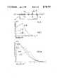
For further clarification of the subject, the harmonic distortion coefficient (non-linear distortion coefficient) of the demodulated signal is graphed in FIGS. 7 and 8 as the function of the number n of the distortion corrector blocks 44-52. The various curves in FIG. 7 in each case relate to different reflection factors ρ. In FIG. 8, the harmonic distortion coefficient in percent is shown for various values of κ (=quotient obtained by dividing the propagation time τ of the reflected wave by the sampling interval). As can be seen, the harmonic distortion coefficient K reaches a vanishingly small value with five distortion corrector blocks.
A significant advantage of the invention consists in that the modified structure for the distortion corrector leads to the remarkable reduction of the hardware expense.
The hardware structure of a distortion corrector is bound by replacing the complex number description used in FIG. 5 and FIG. 6 by real operation. FIG. 9 shows in general form the constitution of an nth distortion corrector block.
The two inputs of the distortion corrector block are resectively connected to a first and a second signal path which respectively contain shift registers 64 and 66. The input of the shift register 64 is connected to a first adding unit 78, while the input of the other shift register 66 is connected to another adding unit 82.
Two multipliers 68 and 70 are connected to the shift register 64. The first multiplier 68 is connected with the first adding unit 76, while the second multiplier 70 is connected with a third adding unit 80 in the second signal path.
At the output of the other shift register 66 is located a third multiplier 72 which is connected to a third adding unit 80 and, furthermore, the output of the shift register 66 is also connected to a fourth multiplier 74 which is connected with the first adding unit 76. The two multipliers 68 and 72 are also provided with the same multiplying factor an, which may be a signal source providing a constant voltage of a magnitude representative of the multiplying factor in question, as symbolically shown in FIG. 9
The advantage obtained by the invention with respect to the expense involved is made clear by comparison of the cascade distortion corrector involved in the apparatus of the invention with the transversal structure of the known recursive filter disclosed for use in the digitial demodulator recommended in the above-mentioned earlier patent application.
In total, 4n multiplications need to be carried out in the use of n cascade blocks such as the distortion corrector blocks 44-52. A comparable transversal distortion corrector has a length of 2n ·κ and therefore requires 4·2n multiplications. The saving in multiplication resulting from the cascade structure used in the invention accordingly amounts to
G=2.sup.n /n
That therefore signifies a factor of 10 for n=6. The number of additions is reduced likewise by such a factor. The capacity of the signal state storage unit is the same in both cases, i.e. a total delay of 2n ·κ sample intervals is needed.
The case of ρ<1 was assumed for the cascade distortion corrector described up to this point, utilizing the distortion corrector blocks 42-52. The cascade system can be extended, however, to include also the case of ρ>1. A modified structure is then to be used for the individual distortion corrector blocks, regarding which FIG. 10 shows for this purpose in schematic representation an nth distortion cvorrector block for ρ>1.
The input signal yn-1 (k) is supplied to a multiplier 84 and also to a delay circuit 88. An adding unit 86 is connected to the multiplier 84 which is also connected with the output of the delay circuit 88.
In the case illustrated by FIG. 10, one more correction multiplication, in this case with the factor r-1-1 ·e+jψ is to be carried out ahead of the first distortion corrector block.
Although the invention has been described with reference to particular illustrative examples, it will be understood that variations and modifications are possible within the inventive concept.
When there is multi-path transmission from a transmitter to a receiver by radio, in addition to the path of direct radiation from the transmitter to the receiver there may be a number of paths involving reflections from ground, buildings, or the like and there may be a refracted wave path higher than the direct path in case of a temperature inversion in the atmosphere. These additional paths involve longer transmission times and the signals received over them are generally referred to as reflected wave components.

Claims (14)

What is claimed is:
1. Demodulator for frequency modulated signals in digital form comprising
an analog-to-digital converter for converting analog frequency modulated signals into digital form and a band-pass filter ahead of the input of said converter and having a narrow pass-band for reduction of adjacent-channel interference, said demodulator further comprising, for suppression of effects of multi-path reception and for compensating for distortion produced by said band-pass filter:
a non-recursive cascade distortion corrector unit connected for filtering digital signals produced by said converter and comprising several (n) distortion corrector blocks connected in tandem one after the other, each of said corrector blocks (44, 46, 48, 50, 52) having an input, signal delay means and multiplier means and being constituted for raising the phase rotation (ψ) and the propagation time (τ) and reducing the reflected wave amplitude (ρ) of signals supplied to the input of the corrector block, each of said corrector blocks delaying, by said signal delay means, said supplied signals for a single interval of time (2n-1 κT) and every said multiplier means in each of said corrector blocks multiplying, by a complex reflection factor, the signals delayed by said delay means.
2. Demodulator according to claim 1, in which said cascade distortion corrector is constituted for responding to a received FM signal disturbed by reflection and having the form ##EQU3## to produce an output signal of the following form: ##EQU4## in which ΔΩ signifies rotary frequency swing; v(t)=modulating low-frequency signal; ρ=amplitude of the reflected wave; ψ=phase rotation of the reflected wave; τ=κ·T= propagation time; T=sampling interval; ρ= angle; χ=quotient obtained by dividing the propagation time of the reflected wave by the sampling interval.
3. Demodulator according to claim 2, in which a second corrector block (46) having its input connected for receiving the output of said first corrector block (44) is constituted for responding to a signal at said input by producing an output which has the form;
y.sub.2 (k)=e.sup.jψ(k) -ρ.sup.4 e.sup.-4jψ e.sup.jψ(k-4κ)                                  ( 3)
4. Demodulator according to claim 3, in which the output of said cascade distortion corrector obtained from the output of the last in cascade of said corrector blocks exhibits the following reflection parameters:
ρ.sub.n =ρ.sup.2 .spsp.n, ψ.sub.n =2.sup.n ψ, κ.sub.n =2.sup.n ·κ,
in which n is the number of corrector blocks in said cascade distortion corrector.
5. Demodulator according to claim 2, in which the output of said cascade distortion corrector obtained from the output of the last in cascade of said corrector blocks exhibits the following reflection parameters:
ρ.sub.n =ρ.sup.2 .spsp.n, ψ.sub.n =2.sup.n ψ, κ.sub.n =2.sup.n ·κ,
in which n is the number of corrector blocks in said cascade distortion corrector.
6. Demodulator according to claim 1, in which the output of said cascade distortion corrector obtained from the output of the last in cascade of said corrector blocks exhibits the following reflection parameters:
ρ.sub.n =ρ.sup.2 .spsp.n, ψ.sub.n =2.sup.n ψ, κ.sub.n =2.sup.n ·κ,
in which n is the number of corrector blocks in said cascade distortion corrector.
7. Demodulator according to claim 1, in which said cascade distortion corrector is constituted with not less than five nor more than six of said distortion corrector blocks.
8. Demodulator according to claim 7 wherein the nth distortion corrector block incorporates a delay of said signals supplied the input thereof, before supplying said signals to said multiplier thereof, which is equal to 2n-1 ·κ·T and in said multiplier said delayed signals are multiplied by the complex reflection factor ρ2.spsp.n-1 ·e-j(2.spsp.n-1.sup.ψ), where n is the ordinal number of the respective distortion corrector in said cascade, ψ is the phase rotation of the reflected wave, κ is the quotient obtained by dividing the propagation time of the reflected wave by the sampling interval and T is the sampling interval.
9. Demodulator according to claim 1, in which each of said corrector blocks of said cascade distortion corrector has two signal paths in each of which there is provided a shift register (64, 66) followed by a first (68, 72) and a second (70, 74) multiplier as well as a first (76, 80) and a second (78, 82) adding unit.
10. Demodulator according to claim 9, in which the signal (yn-1 (k) ) supplied to a first of said shift registers (64) is also supplied to the second adding unit (78) of the same signal path and that the signal supplied to the second shift register (66) is also suplied to the second adding unit (82) of the signal path to which said second shift register pertains.
11. Demodulator according to claim 10, in which the output of said first shift register (64) is connected through said second multiplier (70) in the signal path in which said shift register is located with said first adding unit (80) in the signal path of said second shift register (66) and said output of said second shift register (66) is connected through said second multiplier (74) of the signal path in which said second shift register is located with the first adding unit (76) in the signal path in which said first shift register is located.
12. Demodulator according to claim 1, for coping with received signals in which the refelection amplitude is greater than unity, and in which each corrector block of said cascade distortion corrector is provided with a first signal path in which is located a multiplier (84) and a second signal path in which is located a delay circuit (88), said multiplier (84) and said delay circuit (88) being connected with a common adding unit (86).
13. Demodulator according to claim 12, in which an additional multiplier is provided between the output of said analog-to-digital converter and the first corrector block of said cascade distortion corrector for producing a preliminary correction multiplication of signals by the factor r-1-1 ·e+jψ.
14. Demodulator according to claim 1 wherein the nth distortion corrector block incorporates a delay of said signals supplied the input thereof, before supplying said signals to said multiplier thereof, which is equal to 2n-1 ·κ·T and in said multiplier said delayed signals are multiplied by the complex reflection factor ρ2.spsp.n-1 e-j(2.spsp.n-1.sup.ψ), where n is the ordinal number of the respective distortion corrector in said cascade, ψ is the phase rotation of the reflected wave, κ is the quotient obtained by dividing the propagation time of the reflected wave by the sampling interval and T is the sampling interval.
US06/857,859 1985-05-15 1986-04-30 Demodulator for digital FM signals Expired - Lifetime US4736392A (en)

Applications Claiming Priority (2)

Application Number Priority Date Filing Date Title
DE3517485 1985-05-15
DE19853517485 DE3517485A1 (en) 1985-05-15 1985-05-15 DEMODULATOR FOR FREQUENCY MODULATED SIGNALS IN DIGITAL FORM

Publications (1)

Publication Number Publication Date
US4736392A true US4736392A (en) 1988-04-05

Family

ID=6270777

Family Applications (1)

Application Number Title Priority Date Filing Date
US06/857,859 Expired - Lifetime US4736392A (en) 1985-05-15 1986-04-30 Demodulator for digital FM signals

Country Status (4)

Country Link
US (1) US4736392A (en)
EP (1) EP0201758B1 (en)
JP (1) JP2510992B2 (en)
DE (2) DE3517485A1 (en)

Cited By (15)

* Cited by examiner, † Cited by third party
Publication number Priority date Publication date Assignee Title
US4866649A (en) * 1986-11-12 1989-09-12 Siemens Aktiengesellschaft Multi-dimensional digital filter having adders, multipliers and shift elements
US4947408A (en) * 1989-05-12 1990-08-07 The United States Of America As Represented By The Administrator Of The National Aeronautics And Space Administration Digital carrier demodulator employing components working beyond normal limits
US4955078A (en) * 1987-10-05 1990-09-04 U.S. Philips Corporation Frequency difference detector (FDD) having automatic gain control and a carrier modulated receiver including the FDD
US5014352A (en) * 1987-10-05 1991-05-07 U.S. Philips Corporation Frequency difference detector (FDD) and a carrier modulated receiver including such a FDD
US5068817A (en) * 1987-02-19 1991-11-26 Ant Nachrichtentechnik Gmbh Non-recursive half-band filter with complex valued coefficients for complex input and output signals
US5128966A (en) * 1989-02-15 1992-07-07 Samsung Electronics Co., Ltd. System for demodulating frequency- or phase-modulated signals by quadrature-phase
US5381446A (en) * 1993-06-25 1995-01-10 Digital Wireless Corp. Digital implementation of spread spectrum communications system
US5398002A (en) * 1989-02-15 1995-03-14 Samsung Electronics Co., Ltd. Automatic frequency control system by quadrature-phase in frequency or phase demodulating system
US5430770A (en) * 1994-04-22 1995-07-04 Rockwell International Corp. Method and apparatus for composite signal separation and PSK/AM/FM demodulation
US5493721A (en) * 1992-11-07 1996-02-20 Grundig E.M.V. Receiver for a digital radio signal
US5615411A (en) * 1994-04-22 1997-03-25 Rockwell International Method and apparatus for composite signal separation and FM demodulation
US5694079A (en) * 1996-04-04 1997-12-02 Lucent Technologies Inc. Digital FM demodulator using a lagrangian interpolation function
US6006070A (en) * 1995-04-07 1999-12-21 Telecommunications Equipment Corporation Multi-function interactive communications system with circularly/elliptically polarized signal transmission and reception
US6233435B1 (en) 1997-10-14 2001-05-15 Telecommunications Equipment Corporation Multi-function interactive communications system with circularly/elliptically polarized signal transmission and reception
US20070018867A1 (en) * 2005-07-22 2007-01-25 Semiconductor Technology Academic Research Center Band-pass delta-sigma ad modulator for ad-converting high frequency narrow signal with higher precision and lower consumption power

Families Citing this family (6)

* Cited by examiner, † Cited by third party
Publication number Priority date Publication date Assignee Title
DE3444449A1 (en) * 1984-12-06 1986-06-12 Robert Bosch Gmbh, 7000 Stuttgart DEMODULATOR FOR DIGITAL RECEIVERS
DE3532857A1 (en) * 1985-09-14 1987-03-26 Bosch Gmbh Robert Non-recursive digital filter
DE3543898A1 (en) * 1985-12-12 1987-06-19 Blaupunkt Werke Gmbh EQUALIZER IN THE FORM OF A DIGITAL NON-RECURSIVE FILTER
DE3916426A1 (en) * 1989-05-19 1990-11-22 Blaupunkt Werke Gmbh CAR RADIO WITH A DIGITAL EQUALIZER NETWORK
DE4104882A1 (en) * 1991-02-18 1992-08-20 Blaupunkt Werke Gmbh CAR RADIO WITH A CIRCUIT FOR THE ANALOG / DIGITAL CONVERSION OF AN INTERMEDIATE FREQUENCY SIGNAL
DE4309684C2 (en) * 1992-12-12 1995-11-23 Ant Nachrichtentech Process for demodulating frequency-modulated signals

Citations (6)

* Cited by examiner, † Cited by third party
Publication number Priority date Publication date Assignee Title
US3803501A (en) * 1972-11-17 1974-04-09 Ibm Frequency discriminator using digital non-recursive filters
US3979701A (en) * 1975-06-17 1976-09-07 Communications Satellite Corporation (Comsat) Non-recursive digital filter employing simple coefficients
US4184129A (en) * 1976-06-04 1980-01-15 Agence Nationale De Valorisation De La Recherche (Anvar) Systems for transmitting data between distant locations
US4506228A (en) * 1981-09-26 1985-03-19 Robert Bosch Gmbh Digital FM detector
US4584600A (en) * 1982-10-06 1986-04-22 Itt Industries, Inc. Digital filter for the chrominance channel of a color-television set
DE3444449A1 (en) * 1984-12-06 1986-06-12 Robert Bosch Gmbh, 7000 Stuttgart DEMODULATOR FOR DIGITAL RECEIVERS

Family Cites Families (4)

* Cited by examiner, † Cited by third party
Publication number Priority date Publication date Assignee Title
DE2262652C2 (en) * 1972-12-21 1983-06-30 Licentia Patent-Verwaltungs-Gmbh, 6000 Frankfurt Digital filter bank
JPS5910094B2 (en) * 1978-04-12 1984-03-07 日本電気株式会社 amplitude equalizer
DE3138464A1 (en) * 1981-09-26 1983-04-14 Robert Bosch Gmbh, 7000 Stuttgart Method for the digital demodulation of frequency-modulated signals
DE3302550A1 (en) * 1983-01-26 1984-07-26 Siemens AG, 1000 Berlin und 8000 München Digital linear-phase low-pass filter circuit

Patent Citations (6)

* Cited by examiner, † Cited by third party
Publication number Priority date Publication date Assignee Title
US3803501A (en) * 1972-11-17 1974-04-09 Ibm Frequency discriminator using digital non-recursive filters
US3979701A (en) * 1975-06-17 1976-09-07 Communications Satellite Corporation (Comsat) Non-recursive digital filter employing simple coefficients
US4184129A (en) * 1976-06-04 1980-01-15 Agence Nationale De Valorisation De La Recherche (Anvar) Systems for transmitting data between distant locations
US4506228A (en) * 1981-09-26 1985-03-19 Robert Bosch Gmbh Digital FM detector
US4584600A (en) * 1982-10-06 1986-04-22 Itt Industries, Inc. Digital filter for the chrominance channel of a color-television set
DE3444449A1 (en) * 1984-12-06 1986-06-12 Robert Bosch Gmbh, 7000 Stuttgart DEMODULATOR FOR DIGITAL RECEIVERS

Cited By (16)

* Cited by examiner, † Cited by third party
Publication number Priority date Publication date Assignee Title
US4866649A (en) * 1986-11-12 1989-09-12 Siemens Aktiengesellschaft Multi-dimensional digital filter having adders, multipliers and shift elements
US5068817A (en) * 1987-02-19 1991-11-26 Ant Nachrichtentechnik Gmbh Non-recursive half-band filter with complex valued coefficients for complex input and output signals
US4955078A (en) * 1987-10-05 1990-09-04 U.S. Philips Corporation Frequency difference detector (FDD) having automatic gain control and a carrier modulated receiver including the FDD
US5014352A (en) * 1987-10-05 1991-05-07 U.S. Philips Corporation Frequency difference detector (FDD) and a carrier modulated receiver including such a FDD
US5128966A (en) * 1989-02-15 1992-07-07 Samsung Electronics Co., Ltd. System for demodulating frequency- or phase-modulated signals by quadrature-phase
US5398002A (en) * 1989-02-15 1995-03-14 Samsung Electronics Co., Ltd. Automatic frequency control system by quadrature-phase in frequency or phase demodulating system
US4947408A (en) * 1989-05-12 1990-08-07 The United States Of America As Represented By The Administrator Of The National Aeronautics And Space Administration Digital carrier demodulator employing components working beyond normal limits
US5493721A (en) * 1992-11-07 1996-02-20 Grundig E.M.V. Receiver for a digital radio signal
US5381446A (en) * 1993-06-25 1995-01-10 Digital Wireless Corp. Digital implementation of spread spectrum communications system
US5430770A (en) * 1994-04-22 1995-07-04 Rockwell International Corp. Method and apparatus for composite signal separation and PSK/AM/FM demodulation
US5615411A (en) * 1994-04-22 1997-03-25 Rockwell International Method and apparatus for composite signal separation and FM demodulation
US6006070A (en) * 1995-04-07 1999-12-21 Telecommunications Equipment Corporation Multi-function interactive communications system with circularly/elliptically polarized signal transmission and reception
US5694079A (en) * 1996-04-04 1997-12-02 Lucent Technologies Inc. Digital FM demodulator using a lagrangian interpolation function
US6233435B1 (en) 1997-10-14 2001-05-15 Telecommunications Equipment Corporation Multi-function interactive communications system with circularly/elliptically polarized signal transmission and reception
US20070018867A1 (en) * 2005-07-22 2007-01-25 Semiconductor Technology Academic Research Center Band-pass delta-sigma ad modulator for ad-converting high frequency narrow signal with higher precision and lower consumption power
US7242337B2 (en) * 2005-07-22 2007-07-10 Semiconductor Technology Academic Research Center Band-pass Δ-Σ AD modulator for AD-converting high frequency narrow-band signal with higher precision and lower power consumption

Also Published As

Publication number Publication date
EP0201758A3 (en) 1988-01-13
JPS61264902A (en) 1986-11-22
EP0201758A2 (en) 1986-11-20
JP2510992B2 (en) 1996-06-26
DE3683682D1 (en) 1992-03-12
EP0201758B1 (en) 1992-01-29
DE3517485A1 (en) 1986-11-20

Similar Documents

Publication Publication Date Title
US4736392A (en) Demodulator for digital FM signals
US4506228A (en) Digital FM detector
CN1061489C (en) Direct conversion tuner
US9172416B2 (en) Simplified high frequency tuner and tuning method
EP0540195B1 (en) Digital quadrature radio receiver with two-step processing
US4737658A (en) Centralized control receiver
US5282023A (en) Apparatus for NTSC signal interference cancellation through the use of digital recursive notch filters
US5493721A (en) Receiver for a digital radio signal
US4649507A (en) Segmented transversal filter
JP3122793B2 (en) Method and nonlinear filter for reducing co-channel interference
US6304751B1 (en) Circuits, systems and methods for digital correction of phase and magnitude errors in image reject mixers
DE4326843C2 (en) Receiving method and receiving antenna system for eliminating reusable interference or control device for performing this method
EP0411741A1 (en) Digital equalizer and FM receiver having same
JPH0311814A (en) Ssb modulator and ssb demodulator
US4809203A (en) Hybrid analog-digital filter
JPS61137406A (en) Demoldulator for digital receiver
US4794556A (en) Method and apparatus for sampling in-phase and quadrature components
US4106053A (en) Digital sampling rate conversion of color TV signal
US5768165A (en) Digital time signal filtering method and device for transmission channel echo correction
EP1079523B1 (en) Switched bandwidth digital filters with slewing
CN111416917B (en) Analog television signal processing method and device
EP1184980A2 (en) Digital receiver
GB2282303A (en) Process for the digital generation of a complex baseband signal
CA1182177A (en) Apparatus for testing microwave radios having a 35 mhz if using test equipment designed for 70 mhz if
US7705760B2 (en) Method and device for the filtering and analogue/digital conversion of analogue signal

Legal Events

Date Code Title Description
AS Assignment

Owner name: BLAUPUNKT-WERKE GMBH ROBERT-BOSCH-STRASSE 200 D-32

Free format text: ASSIGNMENT OF ASSIGNORS INTEREST.;ASSIGNORS:KAMMEYER, KARL-DIRK;TOBERGTE, WOLFGANG;REEL/FRAME:004548/0034

Effective date: 19860415

Owner name: BLAUPUNKT-WERKE GMBH, GERMANY

Free format text: ASSIGNMENT OF ASSIGNORS INTEREST;ASSIGNORS:KAMMEYER, KARL-DIRK;TOBERGTE, WOLFGANG;REEL/FRAME:004548/0034

Effective date: 19860415

STCF Information on status: patent grant

Free format text: PATENTED CASE

FPAY Fee payment

Year of fee payment: 4

FEPP Fee payment procedure

Free format text: PAYOR NUMBER ASSIGNED (ORIGINAL EVENT CODE: ASPN); ENTITY STATUS OF PATENT OWNER: LARGE ENTITY

FPAY Fee payment

Year of fee payment: 8

FPAY Fee payment

Year of fee payment: 12