US4742561A - Apparatus for generating signals useful for testing the sensitivity of microwave receiving equipment - Google Patents
Apparatus for generating signals useful for testing the sensitivity of microwave receiving equipment Download PDFInfo
- Publication number
- US4742561A US4742561A US06/774,324 US77432485A US4742561A US 4742561 A US4742561 A US 4742561A US 77432485 A US77432485 A US 77432485A US 4742561 A US4742561 A US 4742561A
- Authority
- US
- United States
- Prior art keywords
- output
- input
- noise
- signal
- power level
- Prior art date
- Legal status (The legal status is an assumption and is not a legal conclusion. Google has not performed a legal analysis and makes no representation as to the accuracy of the status listed.)
- Expired - Lifetime
Links
Images

Classifications
-
- G—PHYSICS
- G01—MEASURING; TESTING
- G01R—MEASURING ELECTRIC VARIABLES; MEASURING MAGNETIC VARIABLES
- G01R29/00—Arrangements for measuring or indicating electric quantities not covered by groups G01R19/00 - G01R27/00
- G01R29/26—Measuring noise figure; Measuring signal-to-noise ratio
-
- G—PHYSICS
- G01—MEASURING; TESTING
- G01R—MEASURING ELECTRIC VARIABLES; MEASURING MAGNETIC VARIABLES
- G01R35/00—Testing or calibrating of apparatus covered by the other groups of this subclass
- G01R35/005—Calibrating; Standards or reference devices, e.g. voltage or resistance standards, "golden" references
- G01R35/007—Standards or reference devices, e.g. voltage or resistance standards, "golden references"
Definitions
- the present invention relates to apparatuses which generate signals useful for testing the sensitivity of microwave receiving equipment. More specifically, the present invention relates to an apparatus which generates output test signal useful for testing the sensitivity of microwave receiving equipment in which there is a predetermined separation between the power level of a noise signal and the power level of a carrier signal which are combined to form the output test signal.
- Present day microwave receiving systems can be configured such that a single microwave antenna is connected to microwave receiving equipment.
- the signals received by the dedicated antenna which are input to the microwave receiving equipment usually have a noise component which accompanies the microwave signal.
- the microwave receiving equipment for any system of this type is generally chosen according to its sensitivity and the expectant signal to noise ratio of the incoming signal. That is, the microwave receiving equipment must have the proper signal to noise sensitivity to be able to distinguish between the microwave signal and noise component of the received signal. If the microwave receiving equipment has a sensitivity below the threshold signal to noise ratio of the incoming signal, the microwave receiving equipment can distinguish between the microwave signal and noise thereby allowing for signal capture. If, however, the sensitivity of the microwave receiving equipment is above the threshold signal to noise ratio of the incoming signal, there will not be signal capture resulting in noise being output from the microwave receiving equipment.
- the prior art discloses systems or devices to test or diagnose certain receiver characteristics but none are useful for testing the purported sensitivity of microwave receiving equipment.
- U.S. Pat. No. 4,004,230 discloses a device for evaluating receiver parameters such as sensitivity, bandpass characteristics and operating frequencies by injecting a modulated signal into the receiver under test.
- U.S. Pat. No. 4,125,809 discloses a system to measure the ratio of carrier power to noise power in a 1 Hz bandwidth of an earth coverage beacon signal.
- Japanese application No. 58-151734 discloses a receiver having a self-diagnosing means which has incorporated therein a noise generator which delivers a self-diagnosing signal to the receiver.
- these systems or devices do not provide a test signal with a fixed separation between carrier and noise power levels which is injected into the microwave receiving equipment under test to test the purported sensitivity of the microwave receiving equipment as does the present invention.
- the present invention is an apparatus which generates an output test signal useful for testing the sensitivity of microwave receiving equipment.
- the test signal output from the apparatus of the invention is a combined signal formed from a noise signal and a carrier signal.
- the output test signal has a predetermined separation between the power level of a noise signal and the power level of a carrier signal that can be varied which when injected into microwave receiving equipment will allow the signal or carrier to noise sensitivity of the microwave receiving equipment under test to be measured.
- the apparatus of the present invention has two noise sources for generating the noise signal portion of the output test signal.
- the first noise source is a naturally excited resistor and the second noise source is a diode energized by a variable voltage source.
- the first noise source, the naturally excited resistor is selected when a passive device is desired.
- the second noise source, the diode is selected when it is desired to generate an output test signal with a greater power level for testing the sensitivity of microwave receiving equipment.
- Both noise sources are connected to a switch which can be positioned to select either noise source dependent on whether the apparatus is to be tested by passive or active tests signals.
- the output of the switch is connected to the input a first amplifier stage.
- This amplifier stage amplifies the power level of the noise signal generated by, for example, the diode noise source.
- the output of the first amplifier stage is connected to the input of a second amplifier stage which like the first amplifier stage amplifies the power level of noise signal.
- the output of the second amplifier stage is input to an attenuator.
- the attenuator is used to attenuate the power level of the noise signal to a predetermined value as will be described.
- the output of the attenuator is input to a third amplifier stage which amplifies the power level of the noise signal output from the attenuator.
- the output of the third stage amplifier is input to a first splitter.
- the noise signal is split into two signals by the first splitter.
- the first signal output from the first splitter is input to a power meter for viewing the power level of the signal received.
- the second signal output from the first splitter is input to a combiner.
- the attenuation of the power level of the noise signal to the desired predetermined value can be viewed by observing the power meter connected to the output of the first splitter previously mentioned. When the desired power level of the noise signal is reached, the attenuation operation is stopped.
- a second splitter receives at its input a carrier signal which forms the second portion of the output test signal of the apparatus of the invention.
- the first signal of the split carrier signal output from the second splitter is input to a power meter for viewing the power level of the carrier signal to determine the exact power level of the carrier signal.
- the second signal of the split carrier signal output from the second splitter is input to the combiner which also receives at another input the second output of the first splitter.
- the combiner combines the noise signal and carrier signal to provide an output test signal with a specific separation between the power levels of the carrier signal and noise signal to be injected into the microwave receiving equipment so that the carrier to noise of the microwave receiving equipment under test can be measured.
- An object of the invention is to provide an apparatus for generating an output test signal useful for testing the carrier to noise and ultimately the signal to noise sensitivity of microwave receiving equipment.
- Another object of the invention is to provide an apparatus for generating an output test signal useful for testing the sensitivity of a microwave receiving equipment in which the output test signal has a predetermined separation between the power level of the noise signal and the power level of the carrier signal indicative of the signal to noise sensitivity of the microwave receiving equipment under test.
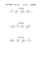
- FIG. 1 shows a schematic diagram of the apparatus of the invention.
- FIG. 2 shows a first alternative dispositon of the attenuator with respect to the amplifier stages.
- FIG. 3 shows a second alternative disposition of the attenuator with respect to the amplifier stages.
- FIG. 4 shows a third alternative disposition of the attenuator with respect to the amplifier stages.
- FIG. 1 a schematic diagram of the apparatus of the present invention is shown.
- the apparatus of the present invention is independent of the microwave receiving equipment under test.
- the apparatus of the invention generates an output test signal having a fixed separation between the power level of a noise signal and the power level of the carrier signal which are combined to form the output test signal.
- the combined signal output from the apparatus of the invention has a specific signal to noise ratio consistent with the purported signal to noise sensitivity of the microwave receiving equipment being tested.
- the microwave receiving equipment has a signal to noise sensitivity consistent with the separation between the power levels of the carrier signal and noise signal of the output test signal from the apparatus of the invention. If, on the other hand, there is no signal capture, the microwave receiving equipment does not have this purported sensitivity.
- noise sources for generating a noise signal in the apparatus of the invention.
- the first is naturally excited resistor 100 and the second is diode 106 energized by variable voltage source 105. Which noise source is selected is determined by switch 104 that can be positioned to select either line 102 connected to naturally excited resister 100 or to line 108 connected to diode noise source 106.
- Noise source 100 is selected when it is desired to generate an output test signal from a passive noise source.
- Resistor 100 is a resistor of the same AC resistance as the input AC resistance of the first stage amplifier. That is, there is impedance matching between the resistor 100 and the stage amplifier. At room temperature, when excited, resistor 100 produces random noise with a power level in the range of -65 to -70 dB.
- switch 104 When it is desired to produce an output test signal with a power level of greater amplitude for testing the sensitivity of microwave receiving equipment, switch 104 is positioned to select line 108 connected to diode 106.
- Variable voltage source 105 which is connected to and energizes diode 106 is a DC source.
- Variable voltage source 105 is variable between 0 and -20 volts.
- the voltage used to energize diode 106 within the above stated range is determined by selection of the voltage which produces a noise signal with the greatest power level. This voltage is approximately -10 volts ⁇ 0.
- Diode 106 is forward biased in line 108 toward variable voltage source 105. When diode 106 is energized, it generates a noise signal on line 108 between diode 106 and the terminal of switch 104 connected to line 108. The noise signal generated on line 108 by diode 106 has a power level of approximately -60 dB. Diode 106 is commercially available from Hewlett Packard, Palo Alto, Calif., and has Model No. HP-346B.
- the noise signal on line 108 having a power level of approximately -60 dB is input to line 110 through switch 104.
- the noise signal on line 110 having a power level of approximately -60 dB is input to first stage microamplifier 112.
- Microamplifier 112 is a gain block amplifier commercially available from Avantek Inc., Santa Clara, Calif., and has Model No. ALD-4201N.
- First stage microamplifier 112 amplifies the power level from approximately -60 dB to approximately -40 dB.
- the output of first stage microamplifier 112 on line 148 is input to second stage microamplifier 114.
- Second stage microamplifier 114 has the same Model No. and manufacturer as first stage microamplifier 112.
- Second stage microamplifier 114 amplifies the power level of the noise signal from approximately -40 dB to approximately -20 dB.
- the output of second stage microamplifier 114 on line 150 is input to attenuator 116. The operation of attenuator 116 will be described subsequent to the description of third stage microamplifier 118.
- the output of attenuator 116 on line 160 is input to a third stage microamplifier 118.
- Third stage microamplifier 118 has the same Model No. and manufacturer as the other two microamplifiers previously described.
- Third stage microamplifier 118 amplifies the output of attenuator 116 from approximately -20 dB to a power level of approximately 0 dBm.
- the noise signal with a power level of approximately 0 dBm on line 170 is input to splitter/combiner 120 configured as a splitter.
- Attenuator 116 which is disposed between second stage microamplifier 114 and third stage microamplifier 118 is used for attenuation of the power level of the amplified noise signal so that the power level of the noise signal output from third stage microamplifier 118 on line 170 has a value of 0 dBm.
- Attenuator 116 has an adjustment range of approximately 3 dB. Within this 3 dB range, attenuator 116 is accurate to 0.01 dB. Attenuator 116 can be of any suitable commercially available type, for example, Model No. 4684-100 from Arra, Inc., Bayshore, N.Y. Although attenuator 116 is shown disposed between second stage amplifier 114 and third stages amplifier 118, it can be disposed before all of the amplifier stages, after all of the amplifier stages or between any two amplifier stages without affecting operation of the apparatus of the invention.
- FIGS. 2, 3 and 4 show the alternative dispositions of attenuator 116 with respect to first amplifier stage 112, second amplifier stage 114, and third amplifier stage 118.
- FIG. 2 shows attenuator 116 disposed before first amplifier stage 112;
- FIG. 3 shows attenuator 116 disposed between first amplifier stage 112 and second amplifier stage 114; and
- FIG. 4 shows attenuator 116 disposed after third amplifier stage 118.
- Splitter 120 which receives the amplified noise signal on line 170 having a power level of 0 dBm splits it into two signals. After the split, a first noise signal is input to power meter 124 and a second noise signal is input to splitter/combiner 138 configured as a combiner. Each output from splitter 120 experiences a calculatable power loss due to splitting of the signal.
- Power meter 124 is viewed to insure that the power level of the first noise signal output from splitter 120 on line 122 has a desired level. Since this signal has the desired power level, the operator knows that the output of third stage microamplifier 118 has a value of 0 dBm because he knows what the power loss was to the signal due to splitting. Likewise, the operator knows the power level of the second noise signal output from splitter 120 on line 126 since this power level is the same as the power level of the first noise signal input to power meter 124 which is monitored.
- Splitter/combiner 120 is commercially available from Narda Microwave Corporation, Hauppauge, New York, and has Model No. 3324-2.
- the three microamplifiers 112, 114 and 118 are bandwidth amplifiers having an operational range in the C band (3.7 to 4.2 GHz). Therefore, besides amplifying the signals, they act as bandpass filters so that only noise within the 3.7 to 4.2 GHz range will passed through the amplifiers.
- Microwave carrier signal 127 is input to line 128 to the apparatus of the invention.
- the carrier signal is usually produced by a separate generator which is plugged into the apparatus of the invention to provide the desired carrier signal.
- Microwave carrier signal 127 on line 128 is input to combiner/splitter 130 configured as a splitter.
- Splitter/combiner 130 has the same Model No. and manufacturer as splitter/combiner 120.
- the carrier signal will be in the C band and compatable with the noise signal generated in the previously described portion of the apparatus of the invention.
- the power level of the carrier signal is such that it would comport with the purported signal to noise sensitivity of the microwave receiving equipment under test.
- the carrier signal having this specific power level is split by splitter 130 with a first carrier signal being input to power meter 134 on line 132 and the second carrier signal being input to combiner 138 on line 136. Since the signal is split, each signal output from splitter 130 experiences a calculatable power level loss. This means that each of the outputs of splitter 130 has a known power level drop. This value is monitored by viewing a power meter 134.
- the two signals namely, the second noise signal from splitter 120 on line 126 having a known power level and the second carrier signal output from splitter 130 on 136 also having known a power level, are input to combiner 138 which combines these signals. Since the power level of the second noise signal is known and the power level of the second carrier signal is also known, there is an absolute difference between the power levels of the noise signal and the carrier signal which is meant to comport with the purported signal to noise sensitivity of the microwave receiving equipment under test.
- the combined signal output from combiner 138 on line 140 is input to the microwave receiving equipment being tested to determine if the purported carrier to noise and thence signal to noise sensitivity of the microwave receiving equipment is accurate.
- the present invention has been described for use in the C band with a specific separation between the power level of the noise signal and the power level of the carrier signal, it is contemplated that different separations between the carrier signal and noise signal power levels can be achieved by the present invention, and the apparatus of the present invention can be configured to operate in other than the C band.
Abstract
Description
Claims (21)
Priority Applications (1)
| Application Number | Priority Date | Filing Date | Title |
|---|---|---|---|
| US06/774,324 US4742561A (en) | 1985-09-10 | 1985-09-10 | Apparatus for generating signals useful for testing the sensitivity of microwave receiving equipment |
Applications Claiming Priority (1)
| Application Number | Priority Date | Filing Date | Title |
|---|---|---|---|
| US06/774,324 US4742561A (en) | 1985-09-10 | 1985-09-10 | Apparatus for generating signals useful for testing the sensitivity of microwave receiving equipment |
Publications (1)
| Publication Number | Publication Date |
|---|---|
| US4742561A true US4742561A (en) | 1988-05-03 |
Family
ID=25100900
Family Applications (1)
| Application Number | Title | Priority Date | Filing Date |
|---|---|---|---|
| US06/774,324 Expired - Lifetime US4742561A (en) | 1985-09-10 | 1985-09-10 | Apparatus for generating signals useful for testing the sensitivity of microwave receiving equipment |
Country Status (1)
| Country | Link |
|---|---|
| US (1) | US4742561A (en) |
Cited By (21)
| Publication number | Priority date | Publication date | Assignee | Title |
|---|---|---|---|---|
| EP0314301A2 (en) * | 1987-09-29 | 1989-05-03 | Hewlett-Packard Company | Apparatus and method for measuring the signal-to-noise ratio |
| US5172064A (en) * | 1991-12-02 | 1992-12-15 | The United States Of America As Represented By The Secretary Of Commerce | Calibration system for determining the accuracy of phase modulation and amplitude modulation noise measurement apparatus |
| US5524281A (en) * | 1988-03-31 | 1996-06-04 | Wiltron Company | Apparatus and method for measuring the phase and magnitude of microwave signals |
| US5537680A (en) * | 1994-12-27 | 1996-07-16 | Insulated Wire Incorporated | Cellular receiver range extender |
| US5610600A (en) * | 1994-06-07 | 1997-03-11 | Koenig; Robert H. | Operation verification system and method for navigational instruments |
| DE19949632A1 (en) * | 1999-10-14 | 2001-04-19 | Rohde & Schwarz | Method for generating a test signal with a predetermined signal / noise ratio on a freely selectable output frequency |
| EP1118873A1 (en) * | 2000-01-21 | 2001-07-25 | Dynex Semiconductor Limited | Testing method and apparatus |
| US6298242B1 (en) * | 1999-07-22 | 2001-10-02 | Qualcomm Inc. | Method and apparatus for reducing frame error rate through signal power adjustment |
| EP0967732B1 (en) * | 1998-06-19 | 2001-10-24 | Lucent Technologies Inc. | Method and apparatus for desensitization of a wireless receiver |
| US6314309B1 (en) | 1998-09-22 | 2001-11-06 | Illinois Superconductor Corp. | Dual operation mode all temperature filter using superconducting resonators |
| US20030038935A1 (en) * | 2001-08-21 | 2003-02-27 | Shing-Kuo Pan | Millimeter-and submillimeter-wave noise generator |
| US6711394B2 (en) | 1998-08-06 | 2004-03-23 | Isco International, Inc. | RF receiver having cascaded filters and an intermediate amplifier stage |
| US20050267716A1 (en) * | 2004-05-25 | 2005-12-01 | Texas Instruments Incorporated | System and method for generating and measuring noise parameters |
| US20080113638A1 (en) * | 2006-11-15 | 2008-05-15 | Michael Thomas Curtin | Controlled signal-to-noise ratio generator circuit |
| US20080254095A1 (en) * | 2007-04-13 | 2008-10-16 | Ma Peter X | Delivery device and method for forming the same |
| CN100544329C (en) * | 2005-01-11 | 2009-09-23 | 华为技术有限公司 | A kind of apparatus and method that obtain correction coefficient of receiver |
| US8421478B2 (en) | 2008-01-25 | 2013-04-16 | International Business Machines Corporation | Radio frequency integrated circuit with on-chip noise source for self-test |
| CN103067070A (en) * | 2013-01-22 | 2013-04-24 | 南京中网卫星通信股份有限公司 | Portable satellite terminal test method and device |
| US8688065B2 (en) * | 2012-08-31 | 2014-04-01 | California Institute Of Technology | Method to measure total noise temperature of a wireless receiver during operation |
| CN104820226A (en) * | 2015-04-29 | 2015-08-05 | 重庆长安汽车股份有限公司 | Test method for navigation signal intensity of automobile navigation system |
| CN106771687A (en) * | 2016-12-22 | 2017-05-31 | 华讯方舟科技(湖北)有限公司 | A kind of device and method for testing the noise after microwave product assembling CAP |
Citations (14)
| Publication number | Priority date | Publication date | Assignee | Title |
|---|---|---|---|---|
| DE1218564B (en) * | 1959-03-04 | 1966-06-08 | Telefunken Patent | Procedure for checking that a radar device is working properly |
| US3731186A (en) * | 1971-06-01 | 1973-05-01 | H Sadel | Radio frequency measurements |
| US3896385A (en) * | 1974-01-29 | 1975-07-22 | Comsat | Method and instrument for measuring interference between angle modulated systems |
| US4004230A (en) * | 1975-12-29 | 1977-01-18 | The United States Of America As Represented By The Secretary Of The Navy | Critical parameter receiver tester |
| US4023104A (en) * | 1975-08-08 | 1977-05-10 | Alpha Engineering Corporation | System for establishing signal level for transmission of a CATV cable |
| US4025854A (en) * | 1975-09-26 | 1977-05-24 | Gte Automatic Electric Laboratories Incorporated | In-service technique for measuring transmission characteristics of a microwave radio link |
| US4048567A (en) * | 1975-12-22 | 1977-09-13 | The Singer Company | Broad band microwave receiver gain calibrator |
| US4074201A (en) * | 1976-07-26 | 1978-02-14 | Gte Sylvania Incorporated | Signal analyzer with noise estimation and signal to noise readout |
| US4095192A (en) * | 1968-03-25 | 1978-06-13 | The United States Of America As Represented By The Secretary Of The Army | Random state generator |
| US4125809A (en) * | 1977-11-09 | 1978-11-14 | The United States Of America As Represented By The Secretary Of The Navy | Digital C/kT meter |
| DE2755221A1 (en) * | 1977-12-10 | 1979-06-13 | Tekade Felten & Guilleaume | PROCEDURE AND CIRCUIT ARRANGEMENT FOR MONITORING A RADIO RECEIVER |
| US4328552A (en) * | 1980-01-17 | 1982-05-04 | Stovall Robert E | Statistical calibration system |
| US4353031A (en) * | 1980-04-14 | 1982-10-05 | Calspan Corporation | Orthogonal signal generator |
| JPS58151734A (en) * | 1982-03-05 | 1983-09-09 | Nec Corp | Signal receiver having self-diagnosing means |
-
1985
- 1985-09-10 US US06/774,324 patent/US4742561A/en not_active Expired - Lifetime
Patent Citations (14)
| Publication number | Priority date | Publication date | Assignee | Title |
|---|---|---|---|---|
| DE1218564B (en) * | 1959-03-04 | 1966-06-08 | Telefunken Patent | Procedure for checking that a radar device is working properly |
| US4095192A (en) * | 1968-03-25 | 1978-06-13 | The United States Of America As Represented By The Secretary Of The Army | Random state generator |
| US3731186A (en) * | 1971-06-01 | 1973-05-01 | H Sadel | Radio frequency measurements |
| US3896385A (en) * | 1974-01-29 | 1975-07-22 | Comsat | Method and instrument for measuring interference between angle modulated systems |
| US4023104A (en) * | 1975-08-08 | 1977-05-10 | Alpha Engineering Corporation | System for establishing signal level for transmission of a CATV cable |
| US4025854A (en) * | 1975-09-26 | 1977-05-24 | Gte Automatic Electric Laboratories Incorporated | In-service technique for measuring transmission characteristics of a microwave radio link |
| US4048567A (en) * | 1975-12-22 | 1977-09-13 | The Singer Company | Broad band microwave receiver gain calibrator |
| US4004230A (en) * | 1975-12-29 | 1977-01-18 | The United States Of America As Represented By The Secretary Of The Navy | Critical parameter receiver tester |
| US4074201A (en) * | 1976-07-26 | 1978-02-14 | Gte Sylvania Incorporated | Signal analyzer with noise estimation and signal to noise readout |
| US4125809A (en) * | 1977-11-09 | 1978-11-14 | The United States Of America As Represented By The Secretary Of The Navy | Digital C/kT meter |
| DE2755221A1 (en) * | 1977-12-10 | 1979-06-13 | Tekade Felten & Guilleaume | PROCEDURE AND CIRCUIT ARRANGEMENT FOR MONITORING A RADIO RECEIVER |
| US4328552A (en) * | 1980-01-17 | 1982-05-04 | Stovall Robert E | Statistical calibration system |
| US4353031A (en) * | 1980-04-14 | 1982-10-05 | Calspan Corporation | Orthogonal signal generator |
| JPS58151734A (en) * | 1982-03-05 | 1983-09-09 | Nec Corp | Signal receiver having self-diagnosing means |
Non-Patent Citations (6)
| Title |
|---|
| "Avalanche Diodes as Transfer Noise Standards," pp. 133-135, Keen, 1971. |
| "Measurement Parameters for Preventative Maintenance," Thomas, pp. 32-35, May 1977. |
| Avalanche Diodes as Transfer Noise Standards, pp. 133 135, Keen, 1971. * |
| Beck, D. et al, "Fading Machine for the Simulation of the Ionosphere", 1965, pp. 74-79. |
| Beck, D. et al, Fading Machine for the Simulation of the Ionosphere , 1965, pp. 74 79. * |
| Measurement Parameters for Preventative Maintenance, Thomas, pp. 32 35, May 1977. * |
Cited By (29)
| Publication number | Priority date | Publication date | Assignee | Title |
|---|---|---|---|---|
| US4837498A (en) * | 1987-09-29 | 1989-06-06 | Hewlett-Packard Company | Method and apparatus for setting the signal-to-noise ratio of a carrier wave |
| EP0314301A3 (en) * | 1987-09-29 | 1991-03-20 | Hewlett-Packard Company | Apparatus and method for measuring the signal-to-noise ratio |
| EP0314301A2 (en) * | 1987-09-29 | 1989-05-03 | Hewlett-Packard Company | Apparatus and method for measuring the signal-to-noise ratio |
| US5524281A (en) * | 1988-03-31 | 1996-06-04 | Wiltron Company | Apparatus and method for measuring the phase and magnitude of microwave signals |
| US5172064A (en) * | 1991-12-02 | 1992-12-15 | The United States Of America As Represented By The Secretary Of Commerce | Calibration system for determining the accuracy of phase modulation and amplitude modulation noise measurement apparatus |
| US5610600A (en) * | 1994-06-07 | 1997-03-11 | Koenig; Robert H. | Operation verification system and method for navigational instruments |
| US5537680A (en) * | 1994-12-27 | 1996-07-16 | Insulated Wire Incorporated | Cellular receiver range extender |
| EP0967732B1 (en) * | 1998-06-19 | 2001-10-24 | Lucent Technologies Inc. | Method and apparatus for desensitization of a wireless receiver |
| US6711394B2 (en) | 1998-08-06 | 2004-03-23 | Isco International, Inc. | RF receiver having cascaded filters and an intermediate amplifier stage |
| US6731960B2 (en) | 1998-09-22 | 2004-05-04 | Isco International, Inc. | Dual operation mode all temperature filter using superconducting resonators with superconductive/non-superconductive mixture |
| US6314309B1 (en) | 1998-09-22 | 2001-11-06 | Illinois Superconductor Corp. | Dual operation mode all temperature filter using superconducting resonators |
| US6298242B1 (en) * | 1999-07-22 | 2001-10-02 | Qualcomm Inc. | Method and apparatus for reducing frame error rate through signal power adjustment |
| DE19949632A1 (en) * | 1999-10-14 | 2001-04-19 | Rohde & Schwarz | Method for generating a test signal with a predetermined signal / noise ratio on a freely selectable output frequency |
| US6782246B1 (en) | 1999-10-14 | 2004-08-24 | Rohde & Schwarz Gmbh & Co. Kg | Method for producing a test signal |
| EP1118873A1 (en) * | 2000-01-21 | 2001-07-25 | Dynex Semiconductor Limited | Testing method and apparatus |
| US20030038935A1 (en) * | 2001-08-21 | 2003-02-27 | Shing-Kuo Pan | Millimeter-and submillimeter-wave noise generator |
| US6844786B2 (en) * | 2001-08-21 | 2005-01-18 | Associated Universities, Inc. | Millimeter- and submillimeter-wave noise generator |
| US20050267716A1 (en) * | 2004-05-25 | 2005-12-01 | Texas Instruments Incorporated | System and method for generating and measuring noise parameters |
| US7177772B2 (en) * | 2004-05-25 | 2007-02-13 | Texas Instruments Incorporated | System and method for generating and measuring noise parameters |
| CN100544329C (en) * | 2005-01-11 | 2009-09-23 | 华为技术有限公司 | A kind of apparatus and method that obtain correction coefficient of receiver |
| US20080113638A1 (en) * | 2006-11-15 | 2008-05-15 | Michael Thomas Curtin | Controlled signal-to-noise ratio generator circuit |
| US7634236B2 (en) * | 2006-11-15 | 2009-12-15 | Northrop Grumman Corporation | Controlled signal-to-noise ratio generator circuit |
| US20080254095A1 (en) * | 2007-04-13 | 2008-10-16 | Ma Peter X | Delivery device and method for forming the same |
| US8421478B2 (en) | 2008-01-25 | 2013-04-16 | International Business Machines Corporation | Radio frequency integrated circuit with on-chip noise source for self-test |
| US8688065B2 (en) * | 2012-08-31 | 2014-04-01 | California Institute Of Technology | Method to measure total noise temperature of a wireless receiver during operation |
| CN103067070A (en) * | 2013-01-22 | 2013-04-24 | 南京中网卫星通信股份有限公司 | Portable satellite terminal test method and device |
| CN104820226A (en) * | 2015-04-29 | 2015-08-05 | 重庆长安汽车股份有限公司 | Test method for navigation signal intensity of automobile navigation system |
| CN106771687A (en) * | 2016-12-22 | 2017-05-31 | 华讯方舟科技(湖北)有限公司 | A kind of device and method for testing the noise after microwave product assembling CAP |
| CN106771687B (en) * | 2016-12-22 | 2023-11-24 | 深圳市华讯方舟卫星产业科技有限公司 | Device and method for testing noise of microwave product after CAP assembly |
Similar Documents
| Publication | Publication Date | Title |
|---|---|---|
| US4742561A (en) | Apparatus for generating signals useful for testing the sensitivity of microwave receiving equipment | |
| US5751149A (en) | Method and apparatus for high frequency time domain reflectometry | |
| US4047121A (en) | RF signal generator | |
| US4926134A (en) | Gain monitoring of distortion cancellation amplifiers in a feedforward linear amplifier | |
| CN102780535A (en) | Intermediate-frequency detection based vector network analyzer power control method | |
| US6393372B1 (en) | Automated frequency stepping noise measurement system | |
| US5168215A (en) | Instantaneous frequency measurement apparatus and method | |
| US3602819A (en) | Sensitivity or noise level measurement circuit and method | |
| US4002969A (en) | Optimum length transmission line discriminator with low noise detector | |
| JPH05122170A (en) | Abnormality monitoring device for outdoor receiving equipment | |
| US4264860A (en) | Resistor measuring apparatus | |
| US3821648A (en) | Automatic noise figure indicator | |
| US4360928A (en) | Non-interfering on-line receiver test system | |
| EP0465178A2 (en) | Device for detecting a plurality of frequencies sent from an exchange | |
| US4023104A (en) | System for establishing signal level for transmission of a CATV cable | |
| CN111711498B (en) | Active antenna's anti-interference performance testing arrangement and system | |
| US3210656A (en) | Swept frequency circuit testing system | |
| US4491973A (en) | Transmitter testing method | |
| US6844715B2 (en) | Synthetic RF detection system and method | |
| JP2001044862A (en) | Receiver provided with intermodulation disturbance detecting means | |
| US4562469A (en) | Method and apparatus for aligning traps in a television receiver | |
| Schaefer | Understanding impulse bandwidth specifications of EMI receivers | |
| US3867694A (en) | Monitoring circuitry for amplitude-measuring system | |
| US4614946A (en) | RF receiver utilizing a multiple echo delay line | |
| KR102217900B1 (en) | Method and Apparatus for Measuring Frequency Response Time for Frequency Change |
Legal Events
| Date | Code | Title | Description |
|---|---|---|---|
| AS | Assignment |
Owner name: HOME BOX OFFICE, INC., 1114 AVENUE OF THE AMERICAS Free format text: ASSIGNMENT OF ASSIGNORS INTEREST.;ASSIGNOR:TIPTON, M. SCOTT;REEL/FRAME:004455/0412 Effective date: 19850823 |
|
| STCF | Information on status: patent grant |
Free format text: PATENTED CASE |
|
| REMI | Maintenance fee reminder mailed | ||
| FEPP | Fee payment procedure |
Free format text: PAYOR NUMBER ASSIGNED (ORIGINAL EVENT CODE: ASPN); ENTITY STATUS OF PATENT OWNER: LARGE ENTITY |
|
| FPAY | Fee payment |
Year of fee payment: 4 |
|
| AS | Assignment |
Owner name: TIME WARNER ENTERTAINMENT COMPANY, L.P., NEW YORK Free format text: ASSIGNMENT OF ASSIGNORS INTEREST.;ASSIGNOR:HOME BOX OFFICE, INC.;REEL/FRAME:006306/0158 Effective date: 19920630 |
|
| FPAY | Fee payment |
Year of fee payment: 8 |
|
| FPAY | Fee payment |
Year of fee payment: 12 |
|
| AS | Assignment |
Owner name: HOME BOX OFFICE, INC., NEW YORK Free format text: ASSIGNMENT OF ASSIGNORS INTEREST;ASSIGNOR:WARNER COMMUNICATIONS INC.;REEL/FRAME:013964/0663 Effective date: 20030331 Owner name: WARNER COMMUNICATIONS INC., NEW YORK Free format text: ASSIGNMENT OF ASSIGNORS INTEREST;ASSIGNOR:TIME WARNER ENTERTAINMENT COMPANY, L.P.;REEL/FRAME:013964/0653 Effective date: 20030331 |
|
| AS | Assignment |
Owner name: WARNER BROS. ENTERTAINMENT INC., CALIFORNIA Free format text: ASSIGNMENT OF ASSIGNORS INTEREST;ASSIGNOR:WARNER COMMUNICATIONS INC. C/O AOL TIME WARNER INC.;REEL/FRAME:014066/0854 Effective date: 20030331 Owner name: WARNER COMMUNICATIONS INC., NEW YORK Free format text: ASSIGNMENT OF ASSIGNORS INTEREST;ASSIGNOR:TIME WARNER ENTERTAINMENT COMPANY, L.P.;REEL/FRAME:014078/0621 Effective date: 20030331 |