US4782490A - Method and a system for multiple error detection and correction - Google Patents

Method and a system for multiple error detection and correction Download PDF

Info

Publication number
US4782490A
US4782490A US07/025,978 US2597887A US4782490A US 4782490 A US4782490 A US 4782490A US 2597887 A US2597887 A US 2597887A US 4782490 A US4782490 A US 4782490A
Authority
US
United States
Prior art keywords
sub
sup
inputs
residue
outputs
Prior art date
Legal status (The legal status is an assumption and is not a legal conclusion. Google has not performed a legal analysis and makes no representation as to the accuracy of the status listed.)
Expired - Fee Related
Application number
US07/025,978
Inventor
Grigory Tenengolts
Current Assignee (The listed assignees may be inaccurate. Google has not performed a legal analysis and makes no representation or warranty as to the accuracy of the list.)
GT TECHNOLOGY Inc A CALIFORNIA CORP
Original Assignee
Cythera Corp
Priority date (The priority date is an assumption and is not a legal conclusion. Google has not performed a legal analysis and makes no representation as to the accuracy of the date listed.)
Filing date
Publication date
Application filed by Cythera Corp filed Critical Cythera Corp
Priority to US07/025,978 priority Critical patent/US4782490A/en
Assigned to CYTHERA CORPORATION, 6056 ELMBRIDGE DRIVE, SAN JOSE, CALIFORNIA 95129 A CA. CORP. reassignment CYTHERA CORPORATION, 6056 ELMBRIDGE DRIVE, SAN JOSE, CALIFORNIA 95129 A CA. CORP. ASSIGNMENT OF ASSIGNORS INTEREST. Assignors: TENENGOLTS, GRIGORY
Priority to KR1019880001444A priority patent/KR880011660A/en
Priority to JP63039325A priority patent/JPS63244935A/en
Assigned to GT TECHNOLOGY, INC., A CALIFORNIA CORP. reassignment GT TECHNOLOGY, INC., A CALIFORNIA CORP. ASSIGNMENT OF ASSIGNORS INTEREST. Assignors: CYTHERA CORPORATION
Application granted granted Critical
Publication of US4782490A publication Critical patent/US4782490A/en
Anticipated expiration legal-status Critical
Expired - Fee Related legal-status Critical Current

Links

Images

Classifications

    • GPHYSICS
    • G06COMPUTING; CALCULATING OR COUNTING
    • G06FELECTRIC DIGITAL DATA PROCESSING
    • G06F11/00Error detection; Error correction; Monitoring
    • HELECTRICITY
    • H03ELECTRONIC CIRCUITRY
    • H03MCODING; DECODING; CODE CONVERSION IN GENERAL
    • H03M13/00Coding, decoding or code conversion, for error detection or error correction; Coding theory basic assumptions; Coding bounds; Error probability evaluation methods; Channel models; Simulation or testing of codes
    • H03M13/03Error detection or forward error correction by redundancy in data representation, i.e. code words containing more digits than the source words
    • H03M13/05Error detection or forward error correction by redundancy in data representation, i.e. code words containing more digits than the source words using block codes, i.e. a predetermined number of check bits joined to a predetermined number of information bits
    • H03M13/13Linear codes
    • H03M13/15Cyclic codes, i.e. cyclic shifts of codewords produce other codewords, e.g. codes defined by a generator polynomial, Bose-Chaudhuri-Hocquenghem [BCH] codes
    • H03M13/151Cyclic codes, i.e. cyclic shifts of codewords produce other codewords, e.g. codes defined by a generator polynomial, Bose-Chaudhuri-Hocquenghem [BCH] codes using error location or error correction polynomials

Definitions

  • the present invention relates to disk data storage systems generally and more specifically to a method and a system for error detection and correction employing an interleaved Reed-Solomon code.
  • Reed-Solomon codes are nonbinary codes that can correct multiple, clustered errors, such as occur in disk data storage systems. In order to use such a code to correct errors in binary data, the data is assembled in groups of m bits. These groups represent symbols from the Galois field GF(2 m ). A Reed-Solomon code that corrects t errors will correct any errors in t groups of length m.
  • every codeword is represented by a code polynomial
  • the code is characterized by the generator polynomial g(x).
  • the degree of a polynomial g(x) is equal to the code redundancy n-k.
  • the period T of a polynomial g(x) (the minimum T, such that g(x) divides x T -1) is equal to the code length. Every code polynomial can be expressed as a multiple of g(x).
  • the received codeword r(x) is divided by g(x). If the remainder is equal to 0, it it assumed that there are no errors. Otherwise, it is concluded that an error has occurred and an error correction routine is invoked.
  • the choice of a generator polynomial g(x) determines the error correction capability and the complexity of the encoding and decoding circuitry.
  • the error correction routine calculates syndromes S i from S(x), the remainder of the division of the received codeword r(x) by the generator polynomial g(x)
  • is a primitive element of the Galois field GF(2 m ).
  • Error locations and values are calculated from error location and error evaluator polynomials, which are computed from the syndromes.
  • the general algorithm to find an error location polynomial is the Berklekamp-Massey algorithm described in Chapter 9 of Error Correcting Codes by Peterson and Weldon, MIT Press, second edition (1972). Once the error location polynomial is computed, the error location is calculated using Chien's search algorithm. Both procedures (Massey-Berklekamp's and Chien's) require a significant number of calculations.
  • the C. Riggle et al system implements a Reed-Solomon code with 10-bit symbols.
  • the redundancy of the code is 17 symbols, i.e. 170 bits.
  • the length of the code is equal to (2 10 -1) symbols.
  • the code can correct errors in up to eight symbols.
  • the decoder of the C. Riggle et al system calculates S(x) using the same circuitry used by the encoder.
  • the check portion d(x) of the received codeword r(x) is stored in a buffer.
  • the data portion of r(x) is encoded using an encoder which produces a checksum d 1 (x).
  • the symbols of d 1 (x) and d(x) are XOR'ed to produce S(x).
  • the C. Riggle et al system needs a substantial amount of memory to store 170 check bits. With 170 check bits, the C. Riggle et al system corrects single burst errors up to 71 bits and double bursts errors up to 31 bits. Additionally, the C. Riggle et al system needs eight combinatorial circuits for multiplication by Galois field elements and 13 half adders.
  • the C. Riggle et al system provides a means for rapidly correcting a single symbol error using log and antilog tables which represent elements of Galois field GF(2 10 ).
  • the two tables need 2*(2 10 -1)*10 bits, i.e. 2558 bytes of ROM.
  • the C. Riggle et al system is not flexible. Using it, one can encode every block of data up to (10*(2 10 -1)-170) bits in length. Independent of block length, the system needs 170 bits of check bits. In many practical situations it is desirable to have a system which can change redundancy dependent on different block size, i.e. use less redundancy for a smaller block size. Moreover, it is desirable that this reconfiguration, from one block size to another, be implemented with a minimum number of electrical components.
  • the U.S. Pat. No. 4,142,174 which issued to C. Chen et al describes a high speed decoding scheme for Reed-Solomon code with 8-bit symbols.
  • the C. Chen et al code corrects errors in three symbols.
  • the C. Chen et al scheme does not use an iterative Berlekamp-Massey algorithm to compute error location polynomial. Instead, it provides a method based on the solution of a system of linear equations to find the coefficients of an error location polynomial. Note that in the case of three symbol errors, solving the system of linear equations requires a significant number of computations.
  • the generator polynomial g(x) of the C. Chen et al system has a form
  • is a primitive element of GF(2 8 ).
  • This polynomial has six coefficients not equal to zero or one. Therefore, the encoder of this polynomial requires six combinatorial circuits to implement multiplication of Galois field elements.
  • ⁇ (x) is an error location polynomial. Since the loop search procedure is used twice, once for each root, the procedure is quite time consuming.
  • a typical error detecting code is the CRC-CCITT code (widely used in data communication) which has a generator polynomial x 16 +x 12 +x 5 +1.
  • the CRC-CCITT code detects all single bursts errors of sixteen bits or less and double bursts errors of four bits or less. It is bit serial.
  • bit serial data transfer might be a drawback.
  • a broad object of the present invention is to provide a fast and economical system for correcting data which has been corrupted during data transmission or storage.
  • Another object of the present invention is to provide an adaptive system which can be reconfigured for a different block size, using less redundancy for smaller block sizes.
  • Another object of the present invention is to provide a simple electrical circuit that implements an encoding scheme which has a high error correcting capability.
  • Another object of the present invention is to provide a simple circuit to check the result of a correction.
  • Another object of the present invention is to provide a method for rapidly solving an error location equation.
  • a further object of the present invention is to provide an error correcting system that can be reconfigured into a fast and economical error detecting system.
  • codewords are made up of data and two groups of check symbols.
  • the first group of check symbols is generated by a correction verification code, which verifies error correction; and, the second group of check symbols is generated by an interleaved Reed-Solomon code with symbols from the Galois field GF(2 8 ), which serves for error correction.
  • the correction verification code is cyclic with a generator polynomial
  • the Reed-Solomon code has a form
  • is a primitive element of the field GF(2 8 ), generated by a polynomial
  • the error correction system decoder uses the first root x 1 of an error location polynomial
  • the detection system which employs a portion of the error correction system circuitry, uses a generalized Hamming cyclic code with a generator polynomial
  • is a root of a primitive polynomial
  • FIG. 1 is a diagram depicting a structure of the interleaved code which is used in this invention
  • FIG. 2 is a block diagram of the presently preferred embodiment in accordance with the present invention of an error detection and correction system.
  • FIG. 3 is a block diagram of the correction verification generator included in the system shown in FIG. 2;
  • FIG. 4 is a block diagram of the encoder/residue generator for block sizes up to 510 bytes included in the system shown in FIG. 2;
  • FIG. 5 is a block diagram of the encoder/residue generator for the block sizes from 511 to 1275 bytes included in the system shown in FIG. 2;
  • FIG. 6 is a block diagram of one of the multiplier circuits used in the encoder/residue generators shown in FIGS. 4 and 5;
  • FIG. 7 is a block diagram of the other one of the multiplier circuits used in the encoder/residue generators shown in FIGS. 4 and 5;
  • FIG. 8 is a block diagram of of an error detection and correction system which utilizes an error-trapping technique for single burst correction in accordance with the present invention.
  • FIG. 9 is a block diagram of an error detection system derived from the encoder/residue generator shown in FIGS. 4 and 5.
  • the present invention uses an interleaved Reed-Solomon code (see the previously mentioned Peterson and Weldon reference). Interleaving is implemented by arranging sequences of the basic codewords into h rows of a rectangular array and then transmitting the code column by column, as shown in FIG. 1.
  • the parameter h is called the degree of interleaving.
  • the polynomial of an interleaved code g(x) is described by the polynomial of the basic code g 0 (x) and the degree of interleaving h as
  • the basic Reed-Solomon code for the error correcting system of the present invention has a generator polynomial of the form ##EQU1## where ⁇ is a primitive element of the Galois field GF(2 m ) and
  • Symbols of this code are m bits wide. This code can correct errors in two symbols.
  • is a root of a primitive polynomial p(x) of degree m over GF(2).
  • the encoder of this code requires only two combinatorial circuits, one to implement the multiplication by ⁇ 9 and the other one to implement the multiplication by ⁇ 54 . By changing the degree of interleaving it is easy to adapt to different block size.
  • the maximum length of the interleaved code is equal to (2 m -1)h symbols.
  • the preferred structure of an error correction and detection system has two different modes for block (record) size.
  • the first (1) is up to 510 bytes in length; and, the second (2) is from 511 bytes to 1275 bytes in length. These two ranges cover practical block sizes.
  • Typical block sizes in storage technology and data communications are 128 and 256 bytes of data (which are covered by the first mode) and 512 and 1024 bytes of data (which are covered by the second mode).
  • the degree of interleaving for the first and second ranges are equal to two and five, accordingly.
  • the degree of the polynomials g 1 (x) and g 2 (x) are equal to eight and twenty, which means that for the first mode of operation (1) eight check symbols are needed; and, for the second mode of operation (2) twenty symbols are needed.
  • the circuitry for both modes employs the same combinatorial circuits for multiplication by ⁇ 9 and ⁇ 54 .
  • the code can correct single burst errors up to 25 bits and double burst errors up to 9 bits. Note that in this mode the code can also correct errors in three bytes 75 percent of the time and errors in four bytes 37.5 percent of the time.
  • the code In the second block size mode (2) the code can correct single burst errors up to 73 bits and double burst errors up to 33 bits.
  • the code can also correct errors in three bytes 96 percent of the time, errors in four bytes 86.4 percent of the time, errors in five bytes 71.04 percent of the time, errors in six bytes 51.84 percent of the time, errors in seven bytes a significant percent of the time, etc. up to errors in ten bytes.
  • the degree of interleaving defines the code length and its correction capability. It is possible to use an interleaving degree equal to three for the second mode of operation.
  • the generator polynomial has the form
  • This code can correct single burst errors up to 41 bits and double burst error up to 17 bits.
  • the redundancy of this code is equal to twelve bytes.
  • the maximum code length is 765 bytes.
  • System 100 is shown to include a three state deriver, which is designated 109; a correction verification generator, designated 110; another three state driver 111; an encoder/residue generator 112; another three state driver 113; a control block 114; still another three state driver 115; a data buffer 116; a half adder 118; a syndrome calculator 120; an error location polynomial calculator 122; an error location calculator 124; an error value calculator 126; a correction iteration counter 128; and a correction verification unit 130.
  • Correction verification generator 110 has a set of inputs selectively coupled to a bus 140 by three state driver 109 to receive externally generated signals representing bytes of data (for encoding in an encoding mode) and representing codewords (data followed by (first) check symbols (1)) (for correction verification in a decoding mode). Additionally, correction verification generator 110 has a set of inputs connected to a bus 142 to receive signals for control and initialization; and a set of outputs connected to a bus 144 upon which the generator develops signals representing bytes of (the first) check symbols (1), following the data, in the encoding mode and (a first) residue (1), in the decoding mode. Bus 144 is selectively coupled to bus 140 by three state driver 111.
  • Encoder/residue generator 112 has a set of inputs connected to bus 142 to receive the control/initialization signals; a set of inputs connected to bus 140 to receive the data signals followed by the check symbol (1) signals, in the encoding mode, and the codeword signals (the data followed by the check symbols (1) followed by (second) check symbols (2)), in the decoding mode; an input connected to a line 150 to receive an iteration controlling signal; a set of outputs connected to a bus 152 upon which the generator develops signals representing bytes of (the second) check symbols (2) in the encoding mode, and representing bytes of (a second) residue (2), in the decoding mode; and an output connected to a line 154 upon which generator 112 develops a signal which indicates the detection of an error.
  • Bus 152 is selectively coupled to bus 140 by three state driver 113.
  • Control block 114 has a pair of inputs each connected to a respective one of a pair of lines, respectively designated 160 and 161, to receive externally generated signals, one controlling the mode of operation (encoding/decoding) and the other controlling the record size (up to 510 bytes or between 511 and 1275 bytes); an input connected to a line 162 to receive an externally generated signal initializing the shift registers of correction verification generator 110 and encoder/residue generator 112 (as will become apparent shortly); and an input connected to a line 163 upon which correction verification iteration counter 128 develops a signal indicating the termination of a correction procedure.
  • block 114 has a set of outputs connected to bus 142 upon which the block develops the control/initialization signals, four outputs each connected to a respective one of four lines, respectively designated 164, 165, 166, and 167, upon which the block develops signals for enabling three state drivers 109, 111, 113, and 115, respectively, and a line 168 upon which the block develops a signal for terminating a correction procedure.
  • Block 114 develops a signal on line 164 which is active to enable three state buffer 109 to couple to correction verification generator 110 data represented by signals developed on bus 140 during encoding.
  • the signal developed on line 164 is inactive while check symbols ((1) and (2)) are being shifted out of correction verification generator 110 and encoder/residue generator 112, respectively.
  • the signal developed on line 164 is active only while data and check symbols (1) are being received by correction verification generator 110.
  • a signal is developed by block 114 on line 165 which is active only during encoding and only active then while check symbols (1) are being shifted out of correction verification generator 110.
  • a signal is developed by block 114 on line 166 which is active only during encoding and only active then while check symbols (2) are being shifted out of encoder/residue generator 112.
  • block 114 develops a signal on line 167 which is active only during decoding and only active then while data is being shifted into data buffer 116.
  • Data buffer 116 has a set of inputs selectively coupled to bus 140 by three state driver 115 to receive the data signals; an input connected to line 168 to receive the signal indicating the termination of the correction procedure; and a set of outputs connected to a bus 172 upon which the buffer develops signals representing the stored data.
  • Half adder 118 has a set of inputs connected to bus 172 to receive the stored data signals; a set of inputs connected to a bus 180 to receive signals representing bytes of data for correcting the stored data; and a set of outputs connected to a bus 182 upon which the adder develops signals representing corrected bytes of data for driving external circuitry.
  • Syndrome calculator 120 is shown to have inputs connected to bus 152 to receive the residue signals and outputs connected to a bus 190.
  • Error location polynomial calculator 122 is shown to have inputs connected to bus 190 and outputs connected to a bus 192.
  • Error location calculator 124 is shown to have inputs connected to bus 192, an input connected to line 168, outputs connected to a bus 194, and an output connected to a line 195.
  • Error value calculator 126 is shown to have inputs connected to buses 190 and 194 and to lines 168 and 195 and outputs connected to bus 180, to a bus 196, and to a line 197.
  • Error location calculator 124 develops on line 195 a signal which when in an inactive state forces error value calculator 126 to develop on bus 180 signals (all zero) which pass through half adder 118 (unchanged) a good byte of data.
  • the signal on line 195 forces onto bus 180 signals which effect correction of the current (bad) byte of data.
  • error value calculator 126 develops on bus 196 signals representing the value of erroneous bytes of data and develops on line 197 a signal which indicates whether each byte is odd or even.
  • Correction iteration counter 128 is shown to have an input connected to line 161, an output connected to line 150 upon which the counter develops the iteration controlling signal and an output connected to line 163 upon which the counter develops the signal indicating the termination of the correction procedure.
  • Correction verification unit 130 is shown to have inputs connected to buses 144,196 and to a line 197 and an output connected to a line 198 upon which the unit develops a signal for indicating to external circuitry an uncorrectable error.
  • correction verification generator 110 encoder/residue generator 112, control block 114, data buffer 116, and half adder 118 are implemented in hardware; while, syndrome calculator 120, error location polynomial calculator 122, error location calculator 124, error value calculator 126, correction iteration counter 128, and a correction verification unit 130 are implemented in firmware.
  • Correction verification generator 110 is shown in FIG. 3 of the drawing to have a number of feedback gates, collectively designated 210; a pair of eight bit wide, serially connected, shift register stages, respectively designated 212 and 214; a half adder 216; a number of output gates, collectively designated 218; and a number of input gates, collectively designated 220.
  • the feedback gates, which are collectively designated 210, are configured to selectively couple the signals developed at the set of outputs of half adder 216 to the set of inputs of the first shift register stage 212.
  • the set of outputs of the second shift register stage 214 are connected to the first set of inputs of half adder 216 to couple the signals developed by the stages to the adder.
  • the output gates which are collectively designated 218, are configured to selectively couple the signals developed at the set of outputs of half adder 216 each to the corresponding line of bus 144.
  • the input gates collectively designated 220, are configured to selectively couple the signals developed on the various lines of bus 140 each to the corresponding input of the other (second) set of half adder 216 inputs.
  • Half adder 216 consists of eight XOR gates.
  • shift register stages 212 and 214 are preset to all ones; and, the feedback gates, which are collectively designated 210, are enabled.
  • the feedback gates (210) are disabled when the check symbols (in the encoding mode) or the residue (in the decoding mode) is shifted out through the output gates, which are collectively designated 218.
  • FIGS. 4 and 5 of the drawing are two configurations of encoder/residue generator 112.
  • FIG. 4 shows the configuration for the first block size mode (1) (up to 510 bytes).
  • FIG. 5 shows the configuration for the second block size mode (2) (between 511 and 1275 bytes).
  • Encoder/residue generator 112 has a number of input gates, collectively designated 302; a number of feedback gates, collectively designated 304; a number of output gates, collectively designated 306; an error detector 308; four half adders, respectively designated 310, 312, 314, and 316; two combinatorial circuits, respectively designated 320 and 322; and a number of shift register stages, which are collectively referred to by the designation 324 and which are divided into four groups of serially connected stages, that are respectively designated 326, 328, 330, and 332.
  • the input gates which are collectively designated 302, are configured to selectively couple the signals developed on the various lines of bus 140 each to the corresponding input of the first set of half adder 310 inputs.
  • Signals for driving the other (second) set of inputs of half adder 310 are developed by the group of shift register stages which are designated 326 and which are connected between the set of outputs of half adder 312 and the inputs of half adder 310.
  • the signals for driving the first set of inputs of half adder 312 are developed by the group of shift register stages which are designated 328 and which are connected between the set of outputs of half adder 314 and the inputs of half adder 312; and, the signals for driving the other set of inputs of half adder 312 are developed by the set of outputs of combinatorial circuit 320.
  • the feedback gates which are collectively designated 304, are configured to selectively couple the signals developed at the set of outputs of half adder 310 both to the set of inputs of combinatorial circuit 320 and to the set of inputs of combinatorial circuit 322.
  • the signals developed at the set of outputs of combinatorial circuit 322 drive the first set of inputs of half adder 314; and, the signals for driving the other set of inputs of half adder 314 are developed by the group of shift register stages which are designated 330 and which are connected between the set of outputs of half adder 316 and the inputs of half adder 314.
  • the signals developed at the set of outputs of combinatorial circuit 320 drive the first set of inputs of half adder 316; and, the signals for driving the other set of inputs of half adder 316 are developed by the group of shift register stages which are designated 332 and which are connected between the outputs of half adder 310 and the inputs of half adder 316.
  • the output gates which are collectively designated 306, are configured to selectively couple the signals developed at the set of outputs of half adder 310 each to the corresponding line of bus 152. Also driven by the signals developed at the set of outputs of half adder 310, error detector 308 develops the signal on line 154.
  • Each of the half adders (310, 312, 314, and 316) have eight XOR gates.
  • Combinatorial circuit 320 implements multiplication by ⁇ 54 ; and, combinatorial circuit 322 implements multiplication by ⁇ 9 , both in the Galois field GF(2 8 ), generated by the polynomial x 8 +x 6 +x 5 +x 4 +1.
  • the shift register stages (324) are each eight bit wide. The buses each have eight lines.
  • the encoder/residue generators (112 and 112') of FIGS. 4 and 5 differ in the number of shift register stages in a group, generator 112 having two stages per group and generator 112' having five stages per group.
  • the process of encoding/decoding includes setting the stages of shift register 324 to all ones and serially shifting bytes of data/check symbols from bus 140, through the input gates, which are designated 302, and into the stages of the shift register, while the feedback gates, that are designated 304, are enabled.
  • the check symbols (2) (in case of encoding) or the residue (2) (in case of decoding) is located in the stages of shift register 324 (in stages x 0 , x 1 , x 2 , . . . ).
  • the process includes the step of shifting the check symbols (2)/residue (2) through the stages of shift register 324, through the output gates, which are designated 306, and on to bus 152, while the feedback gates, that are designated 304, are disabled.
  • error detector 308 develops on line 154, the signal which indicates whether an error was detected.
  • encoder/residue generator 112 only has four half adders (310, 312, 314, and 316).
  • Combinatorial circuits 320 and 322 are presented in FIGS. 6 and 7. These circuits implement multiplication of an element
  • x (x 0 , x 1 , x 2 , . . . , x 7 )
  • signals representing bytes of data are externally generated on bus 140 and are shifted byte serially into correction verification generator 110 and encoder/residue generator 112. Responsive thereto, correction verification generator 110 develops on bus 144 signals representing bytes of (the first) check symbols (1), which are shifted byte serially into encoder/residue generator 112 immediately following the data. Responsive to the data and to the check symbols (1) as "data”, encoder/residue generator 112 calculates (the second) check symbols (2) and develops on bus 152 signals representing the (second) check symbols (2) shifted out byte serially.
  • the second group of check symbols (2) serves to provide a means for error correction.
  • the first group of check symbols (1) consists of two bytes which are simple byte parity checks for odd and even data bytes. They (the first group of check symbols) only serve to provide a means for correction verification. They are calculated from the data symbols using a cyclic code with a generator polynomial
  • signals representing bytes of codewords are externally generated on bus 140 and are shifted byte serially into correction verification generator 110, encoder/residue generator 112, and data buffer 116.
  • correction verification generator 110 develops on bus 144 the signals representing the (first) residue (1).
  • encoder/residue generator 112 develops on bus 152 the signals representing the (second) residue (2) and the signal on line 154 which indicates whether an error was detected.
  • Correction iteration counter 128 defines the number of iterations (two--in case of block size up to 510 bytes--and five--in case of block size between 511 and 1275 bytes) controlled by the signal developed on line 150.
  • S 0 , S 1 , S 2 , S 3 are the contents of the appropriate stages of the shift register of encoder/residue generator 112 (shown in FIGS. 4 and 5)).
  • the calculation is performed by syndrome calculator 120. Then the standard test for detecting a single symbol error is executed. If the condition
  • error location polynomial calculator 122 calculates the coefficients of the polynomial (7)
  • error location calculator 124 finds the error locations; and, error value calculator 126 finds the error values.
  • the signal developed by correction iteration counter 128 on line 163 is used to terminate the correction procedure.
  • the error location and error value is used to correct the data coming out of data buffer 116.
  • correction verification unit 130 If error location calculator 124 and error value calculator 126 find no errors in the data and check symbols, the data is considered correct. Otherwise, correction verification unit 130 is invoked. On the basis of error values and locations, correction verification unit 130 calculates two bytes V 1 and V 2 . The two bytes are bit by bit sums by modulo two of error values in odd and even data bytes and check symbols bytes (1), respectively, calculated by error location calculator 124 and error value calculator 126. Correction verification unit 130 compares V 1 and V 2 with bytes V 1 and V 2 which are odd and even bytes of the residue calculated by correction verification generator 110. If
  • system 100 only requires 512 bytes of ROM for log and antilog tables for multiplication and division in Galois field GF(2 8 ). Using these tables, multiplication and division in Galois field GF(2 8 ) are reduced to summation and subtraction by modulo 255. Also, note that correction verification generator 110 calculates bytes V 1 and v 2 simultaneously with the calculation of error locations and values avoiding any additional delay. Further, error location calculator 124 only uses a loop search procedure to find the first root x 1 of the equation
  • the second root is defined as
  • error location calculator 124 calculates the erroneous byte location N in the form
  • R is the data block size and h is the degree of code interleaving.
  • j i (j i .sbsb.7, j i .sbsb.6, . . . , j i .sbsb.0)
  • the decoding can be implemented using an error trapping technique (see, for example, Lin G., Costello D. J. Jr. Error Control coding: Fundamental and applications, Prentice-Hall, 1983). Since single burst errors are confined to (n-k)/2 consecutive symbols, such an error trapping technique is employed in the embodiment of the error detection and correction system of the present invention which is shown in FIG. 8 of the drawing generally designated by the number 800. Like system 100, (shown in FIG.
  • system 800 includes a three state driver 109', a correction verification generator 110', three more three state drivers 111', 113', and 115', a data buffer 116', and a half adder 118', each of which is similiar to the corresponding component of system 100.
  • system 800 includes an encoder/residue generator 812, a control block 814, a residue buffer 816, a three state driver 818, an error trapping correction unit 820, a firmware correction unit 822, and a single burst correction verification unit 824.
  • Encoder/residue generator 812 differs from generator 112 (shown in FIG. 2) in that generator 812 has an additional input connected to a line 830.
  • Control block 814 differs from block 114 in that block 814 has three additional inputs, each connected to the respective one of three lines, respectively designated 832, 834, and 836. Also, block 814 has three additional outputs, one connected to a line 838, another connected to line 830, and the third connected to a line 840. Block 814 develops on line 838 a signal for initiating correction by firmware correction unit 822 and develops on line 830 a signal which is active during preshifting and shifting of encoder/residue generator 812.
  • Residue buffer 816 is shown to have inputs connected to bus 152' to receive the residue signals and outputs connected to a bus 842.
  • Error trapping correction unit 820 is shown to have an input connected to line 830, another input connected to line 168', and a set of inputs selectively coupled to bus 152' by three state driver 818.
  • unit 820 has an output connected to line 834, another output connected to line 832, still another output connected to a line 844, a set of outputs connected to bus 180' and another set of outputs connected to a bus 846.
  • Unit 820 has a displacement counter for counting the number of shifts s of the shift register of encoder/residue generator 812.
  • Firmware correction unit 822 is shown to have an input connected to line 838, a set of inputs connected to bus 842, an output connected to a line 850, and a set of outputs connected to bus 180'. Unit 822 implements in firmware the decoding procedure (including correction verification) described in connection with FIG. 2.
  • Single burst correction verification unit 824 is shown to have an input connected to line 844, a set of inputs connected to buses 846 and 144', an output connected to line 842, and an output connected to line 836.
  • Unit 824 differs from correction verification unit 130 (shown in FIG. 2) in that unit 824 has an additional output and is connected differently.
  • Encoding proceeds as with system 100 (shown in FIG. 2).
  • the residue represented by the signals developed by encoder/residue generator 812 on bus 152' is saved in residue buffer 816. Error trapping correction unit 820 is then invoked.
  • stages x 7 , x 6 , x 5 , x 4 (in the first mode) or in stages x 19 , x 18 , . . .
  • x 10 (in the second mode) correspond to the error pattern in bytes s+1, s+2, s+3, s+4 (in the first mode) or bytes s+1, s+2, . . . , s+10 (in the second mode). (Note that the first byte of data is byte 1).
  • the results of the correction is checked by single burst correction verification unit 824. If after R+2+2h shifts, stages x 0 , x 1 , x 2 , x 3 (in the first mode) or stages x 0 , x 1 , . . .
  • error trapping correction unit 820 develops an active level signal on line 834, causing control block 814 to develop an active level signal on line 838 initiating correction by firmware correction unit 822. If stages x 0 , x 1 , x 2 , x 3 (in the first mode) or stages x 0 , x 1 , . . . , x 9 (in the second mode) all contain zeros, error trapping correction unit 820 develops an active level signal on line 832, causing control block 814 to develop an active level signal on line 840 transferring single burst bytes through three state driver 818 into unit 820.
  • single burst correction verfication unit 824 develops an active level signal on line 842.
  • control block 814 develops an active level signal on line 168' initiating the transfer of data from data buffer 116' and starting the process of decrementing the displacement counter of error trapping correction unit 820. While the displacement counter of error trapping correction unit 820 has a nonzero value, signals developed by unit 820 on bus 180' are forced to all zeros, passing good data, unchanged, through half adder 118'. When the displacement counter of error trapping correction unit 820 reaches zero, erroneous bytes are shifted out of error trapping correction unit 820 onto bus 180' effecting correction of the bytes coming out of data buffer 116'.
  • single burst correction unit 824 develops an active level signal on line 836 causing control block 814 to develop an active level signal on line 838 initiating correction by firmware correction unit 822. If the results of the correction by firmware correction unit 822 are not valid, the unit develops an active level signal on line 850. Otherwise, an active level signal is developed on line 168' initiating transfer of the data from data buffer 116' and XORing appropriate bytes of the data with the bytes forced out of firmware correction unit 822 onto bus 180'.
  • clock periods employed in decoding are shorter than clock periods employed in data transfer (for example, 1/4 of the data transfer clock periods). This allows a single burst correction to be performed in the record transfer time.
  • System 100 (presented in FIG. 2) is much faster at decoding than system 800 (presented in FIG. 8). However, system 100 has more complicated circuitry than system 800. Even though slower than system 100, system 800 is faster than typical error correction systems in which decoding is implemented completely in firmware. Since single burst errors are the errors most frequently encountered in magnetic storage, the system 800 is attractive for magnetic disk and tape applications. Additionally, both systems (100 and 800) are efficient in data storage and communication applications.
  • an error detection code is employed which is symbols (bytes) serial for a high data transfer rate.
  • a basic polynomial g 0 (x) of an interleaved Reed-Solomon code is employed, one which has a minimal number of nonzero coefficients and which can be implemented using the above hardware.
  • the code is a generalized Hamming code.
  • the code is a generalized Hamming code.
  • an encoder results for the generalized Hamming code, which corrects single symbol or detects double symbol errors.
  • the code with the generator polynomial, satisfying the conditions (13) and (14) is a generalized Hamming code.
  • This code has the following important property which characterizes its single burst detection capability.
  • a code with a generator polynomial that satisfies the conditions (13 and (14) detects all single bursts of 16 bits or less.
  • the minimum length single burst, which could't be detected, should have a polynomial representation in the form
  • l 1 is the length of a portion of the burst located in the first of three consecutive bytes and l 2 is the length of a portion of the burst located in the last byte.
  • condition (14) which satisfies the condition (14) has the same single burst detection capability as the 16 bit CRC-CCITT code typically used for error detection. It can detect double bursts of one bit length, since it detects any error in two bytes.
  • FIG. 9 An encoder/residue generator for this code is presented in FIG. 9.
  • This encoder/residue generator is similar to the encoders/residue generators of FIGS. 4 and 5. The only difference is that shift register 324" of FIG. 9 has only two stages: x 0 and x 1 .
  • the presented detection system may be successfully used in data communication systems.
  • bit serial CRC is implemented with parallel circuits.
  • parallel circuits See, for example, "Parallel CRC Lets Many Lines Use One Circuit", by A. K. Pandeya, Computer Design, September 1975, vol. 14, No. 9, p. 87-91.
  • the presented system which employs a nonbinary Hamming code, has a propagation delay less than a system which employs a parallel implementation of the bit serial CRC.
  • the presented system has an XORing depth of degree three.
  • a parallel implementaton of CRC-CCITT has an XORing depth of degree six.
  • the presented system is twice as fast as a parallel implementation of CRC-CCITT.

Abstract

Disclosed is a method and a system for error detection and correction in which codewords are made up of data and two groups of check symbols. The first group of check symbols is generated by a correction verification code, which verifies error correction; and, the second group of check symbols is generated by an interleaved Reed-Solomon code with symbols from the Galois field GF(28), which serves for error correction.
The correction verification code is cyclic with a generator polynomial
g.sub.v (x)=x.sup.2 +1
over the field GF(28).
The Reed-Solomon code has a form
g.sub.0 (x)=x.sup.4 +α.sup.54 x.sup.3 +α.sup.9 x.sup.2
54 x+1,
where α is a primitive element of the field GF(28), generated by a polynomial
p(x)=x.sup.8 +x.sup.6 +x.sup.5 +.sup.4 +1.
The error correction system decoder uses the first root x1 of an error location polynomial
σ(x)=x.sup.2 +σ.sub.1 x+σ.sub.2
to calculate the second root x2 of the polynominal.
The detection system, which employs a portion of the error correction system circuitry, uses a generalized Hamming cyclic code with a generator polynomial
g.sub.d (x)=x.sup.2 +α.sup.9 x+1
where α is a root of a primitive polynomial
p(x)=x.sup.8 +x.sup.6 +x.sup.5 +x.sup.4 +1
over the field GF(2).

Description

TECHNICAL FIELD
The present invention relates to disk data storage systems generally and more specifically to a method and a system for error detection and correction employing an interleaved Reed-Solomon code.
BACKGROUND ART
Reed-Solomon codes are nonbinary codes that can correct multiple, clustered errors, such as occur in disk data storage systems. In order to use such a code to correct errors in binary data, the data is assembled in groups of m bits. These groups represent symbols from the Galois field GF(2m). A Reed-Solomon code that corrects t errors will correct any errors in t groups of length m.
In a Reed-Solomon code, every codeword is represented by a code polynomial
C(x)=c.sub.n-1 x.sup.n-1 +c.sub.n-2 x.sup.n+2 + . . . +c.sub.0,
where
c0, c1, . . . , and cn-k-1
are check symbols and
cn-k, cn-k+1, . . . , and cn-1
are data symbols. The code is characterized by the generator polynomial g(x). The degree of a polynomial g(x) is equal to the code redundancy n-k. The period T of a polynomial g(x) (the minimum T, such that g(x) divides xT -1) is equal to the code length. Every code polynomial can be expressed as a multiple of g(x).
The check symbols
c0, c1, c2, . . . , and cn-k-1
are generated from data symbols
cn-1, cn-2, . . . , and cn-k
by dividing the "data" polynomial
x.sup.n-k (c.sub.n-1 x.sup.k-1 +c.sub.n-2 x.sup.k-2 + . . . +c.sub.n-k+1 x+c.sub.n-k)
by g(x). The "check" polynomial
c.sub.n-k-1 x.sup.n-k-1 +c.sub.n-k-2 x.sup.n-k-2 + . . . +c.sub.1 x+c.sub.0
is the "remainder" of this division.
In decoding, the received codeword r(x) is divided by g(x). If the remainder is equal to 0, it it assumed that there are no errors. Otherwise, it is concluded that an error has occurred and an error correction routine is invoked.
The choice of a generator polynomial g(x) determines the error correction capability and the complexity of the encoding and decoding circuitry.
By reducing the number of different nonzero coefficients of the generator polynomial g(x), the number of electrical circuit components for encoding and decoding (error detection) can be reduced.
The error correction routine calculates syndromes Si from S(x), the remainder of the division of the received codeword r(x) by the generator polynomial g(x)
S.sub.i =S(α.sup.i),
where
S(x)=r(x) mod g(x) and α.sup.i
are roots of the polynomial g(x), α is a primitive element of the Galois field GF(2m).
Error locations and values are calculated from error location and error evaluator polynomials, which are computed from the syndromes. The general algorithm to find an error location polynomial is the Berklekamp-Massey algorithm described in Chapter 9 of Error Correcting Codes by Peterson and Weldon, MIT Press, second edition (1972). Once the error location polynomial is computed, the error location is calculated using Chien's search algorithm. Both procedures (Massey-Berklekamp's and Chien's) require a significant number of calculations.
These procedures are a part of the multiple error correction system described in the U.S. Pat. No. 4,413,339, which issued to C. Riggle et al. The C. Riggle et al system implements a Reed-Solomon code with 10-bit symbols. The redundancy of the code is 17 symbols, i.e. 170 bits. The length of the code is equal to (210 -1) symbols. The code can correct errors in up to eight symbols. The decoder of the C. Riggle et al system calculates S(x) using the same circuitry used by the encoder. The check portion d(x) of the received codeword r(x) is stored in a buffer. The data portion of r(x) is encoded using an encoder which produces a checksum d1 (x). The symbols of d1 (x) and d(x) are XOR'ed to produce S(x). Note, that the C. Riggle et al system needs a substantial amount of memory to store 170 check bits. With 170 check bits, the C. Riggle et al system corrects single burst errors up to 71 bits and double bursts errors up to 31 bits. Additionally, the C. Riggle et al system needs eight combinatorial circuits for multiplication by Galois field elements and 13 half adders.
The C. Riggle et al system provides a means for rapidly correcting a single symbol error using log and antilog tables which represent elements of Galois field GF(210). However, the two tables need 2*(210 -1)*10 bits, i.e. 2558 bytes of ROM.
The C. Riggle et al system is not flexible. Using it, one can encode every block of data up to (10*(210 -1)-170) bits in length. Independent of block length, the system needs 170 bits of check bits. In many practical situations it is desirable to have a system which can change redundancy dependent on different block size, i.e. use less redundancy for a smaller block size. Moreover, it is desirable that this reconfiguration, from one block size to another, be implemented with a minimum number of electrical components.
The U.S. Pat. No. 4,142,174, which issued to C. Chen et al describes a high speed decoding scheme for Reed-Solomon code with 8-bit symbols. The C. Chen et al code corrects errors in three symbols. The C. Chen et al scheme does not use an iterative Berlekamp-Massey algorithm to compute error location polynomial. Instead, it provides a method based on the solution of a system of linear equations to find the coefficients of an error location polynomial. Note that in the case of three symbol errors, solving the system of linear equations requires a significant number of computations.
The generator polynomial g(x) of the C. Chen et al system has a form
g(x)=(x+1)(x+α)(x+α.sup.2)(x+α.sup.3)(x+α.sup.4)(x+α.sup.5),
where α is a primitive element of GF(28). This polynomial has six coefficients not equal to zero or one. Therefore, the encoder of this polynomial requires six combinatorial circuits to implement multiplication of Galois field elements.
In the U.S. Pat. No. 4,360,916, which issued to S. Kustedjo et al. and the U.S. Pat. No. 4,498,175, which issued to M. Nagumo et al., a loop search procedure is disclosed to find both roots x1 and x2 of an equation
σ(X)=0,
where σ(x) is an error location polynomial. Since the loop search procedure is used twice, once for each root, the procedure is quite time consuming.
In disk data storage systems, data is commonly protected by an error correcting code, while the associated header is commonly protected by an error detecting code. A typical error detecting code is the CRC-CCITT code (widely used in data communication) which has a generator polynomial x16 +x12 +x5 +1. The CRC-CCITT code detects all single bursts errors of sixteen bits or less and double bursts errors of four bits or less. It is bit serial.
For systems with high data transfer rate, bit serial data transfer might be a drawback.
For additional background information, the reader is referred to Error Correcting Codes by Peterson and Weldon, MIT Press, Cambridge, Mass., second edition (1972); Error Control Coding; Fundamental And Application by G. Lin and D. J. Costello, Prentice-Hall, Inc., Englewood Cliffs, N.J., 1983 edition; "Interface Between Data Terminal Equipment (DTE) And Data Circuit-Terminating Equipment (DCE) For Terminal Operations In Packet Mode On Public Networks", CCITT Recommendation X.25, With Plenary Assembly, Doc. 7, Geneva, Switzerland, 1980; and "Parallel CRC Lets Many Lines Use One Circuit", by A. K. Pandeya, Computer Design, September 1975, vol. 14, No. 9, p. 87-91.
DISCLOSURE OF THE INVENTION
Accordingly, a broad object of the present invention is to provide a fast and economical system for correcting data which has been corrupted during data transmission or storage.
Another object of the present invention is to provide an adaptive system which can be reconfigured for a different block size, using less redundancy for smaller block sizes.
Another object of the present invention is to provide a simple electrical circuit that implements an encoding scheme which has a high error correcting capability.
Another object of the present invention is to provide a simple circuit to check the result of a correction.
Another object of the present invention is to provide a method for rapidly solving an error location equation.
A further object of the present invention is to provide an error correcting system that can be reconfigured into a fast and economical error detecting system.
These and other objects of the present invention are realized by a method and a system for error detection and correction in which codewords are made up of data and two groups of check symbols. The first group of check symbols is generated by a correction verification code, which verifies error correction; and, the second group of check symbols is generated by an interleaved Reed-Solomon code with symbols from the Galois field GF(28), which serves for error correction.
The correction verification code is cyclic with a generator polynomial
g.sub.v (x)=x.sup.2 +1
over the field GF(28).
The Reed-Solomon code has a form
g.sub.0 (x)=x.sup.4 +α.sup.54 x.sup.3 +α.sup.9 x.sup.2 +α.sup.54 x+1,
where α is a primitive element of the field GF(28), generated by a polynomial
p(x)=x.sup.8 +x.sup.6 +x.sup.5 +x.sup.4 +1.
The error correction system decoder uses the first root x1 of an error location polynomial
σ(x)=x.sup.2 +σ.sub.1 x+σ.sub.2
to calculate the second root x2 of the polynomial.
The detection system, which employs a portion of the error correction system circuitry, uses a generalized Hamming cyclic code with a generator polynomial
g.sub.d (x)=x.sup.2 +α.sup.9 x+1,
where α is a root of a primitive polynomial
p(x)=x.sup.8 +x.sup.6 +x.sup.5 +x.sup.4 +1
over the field GF(2).
These and other objects of the present invention will no doubt become apparent to those skilled in the art after having read the detailed description of the presently preferred method and system of the present invention which are illustrated in the figures of the drawing.
BRIEF DESCRIPTION OF THE FIGURES IN THE DRAWINGS
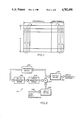
FIG. 1 is a diagram depicting a structure of the interleaved code which is used in this invention;
FIG. 2 is a block diagram of the presently preferred embodiment in accordance with the present invention of an error detection and correction system.
FIG. 3 is a block diagram of the correction verification generator included in the system shown in FIG. 2;
FIG. 4 is a block diagram of the encoder/residue generator for block sizes up to 510 bytes included in the system shown in FIG. 2;
FIG. 5 is a block diagram of the encoder/residue generator for the block sizes from 511 to 1275 bytes included in the system shown in FIG. 2;
FIG. 6 is a block diagram of one of the multiplier circuits used in the encoder/residue generators shown in FIGS. 4 and 5;
FIG. 7 is a block diagram of the other one of the multiplier circuits used in the encoder/residue generators shown in FIGS. 4 and 5;
FIG. 8 is a block diagram of of an error detection and correction system which utilizes an error-trapping technique for single burst correction in accordance with the present invention; and
FIG. 9 is a block diagram of an error detection system derived from the encoder/residue generator shown in FIGS. 4 and 5.
BEST MODE FOR CARRYING OUT THE INVENTION
The present invention uses an interleaved Reed-Solomon code (see the previously mentioned Peterson and Weldon reference). Interleaving is implemented by arranging sequences of the basic codewords into h rows of a rectangular array and then transmitting the code column by column, as shown in FIG. 1. The parameter h is called the degree of interleaving. The polynomial of an interleaved code g(x) is described by the polynomial of the basic code g0 (x) and the degree of interleaving h as
g(x)=g.sub.0 (x.sup.h).
The basic Reed-Solomon code for the error correcting system of the present invention has a generator polynomial of the form ##EQU1## where α is a primitive element of the Galois field GF(2m) and
v=2.sup.m-1 -2, m≧2.
Symbols of this code are m bits wide. This code can correct errors in two symbols.
Note that in order to correct errors in t symbols a generator polynomial of a code should have 2t consecutive roots
α.sup.v, α.sup.v+1, . . . , α.sup.v+2t-1.
By choosing v equal to 2m-1 -2, g0 (x) is made reversible, halving the number of nonzero coefficients. The above polynomial
g.sub.0 (x)=(x+α.sup.v)(x+α.sup.v+1)(x+α.sup.v+2)(x+α.sup.v+3)
can be rewritten in the form
g.sub.0 (x)=x.sup.4 +α.sup.a x.sup.3 +α.sup.b x.sup.2 +α.sup.a x+1,                                       (1)
where α is a root of a primitive polynomial p(x) of degree m over GF(2). The preferred embodiment employs 8-bit wide symbols, i.e. m=8 and v=126. Also in the preferred embodiment
p(x)=x.sup.8 +x.sup.6 +x.sup.5 +x.sup.4 +1, a=54, b=9.
The encoder of this code requires only two combinatorial circuits, one to implement the multiplication by α9 and the other one to implement the multiplication by α54. By changing the degree of interleaving it is easy to adapt to different block size.
The maximum length of the interleaved code is equal to (2m -1)h symbols.
The preferred structure of an error correction and detection system has two different modes for block (record) size. The first (1) is up to 510 bytes in length; and, the second (2) is from 511 bytes to 1275 bytes in length. These two ranges cover practical block sizes. Typical block sizes in storage technology and data communications are 128 and 256 bytes of data (which are covered by the first mode) and 512 and 1024 bytes of data (which are covered by the second mode).
The degree of interleaving for the first and second ranges are equal to two and five, accordingly.
The generator polynomials g1 (x) and g2 (x) for these two modes have the following form
g.sub.1 (x)=g.sub.0 (x.sup.2)=x.sup.8 +α.sup.54 x.sup.6 +α.sup.9 x.sup.4 +α.sup.54 x.sup.2 +1         (2)
and
g.sub.2 (x)=g.sub.0 (x.sup.5)=x.sup.20 +α.sup.54 x.sup.15 +α.sup.9 x.sup.10 +α.sup.54 x.sup.5 +1.       (3)
As can be seen from (2) and (3), the degree of the polynomials g1 (x) and g2 (x) are equal to eight and twenty, which means that for the first mode of operation (1) eight check symbols are needed; and, for the second mode of operation (2) twenty symbols are needed. The circuitry for both modes employs the same combinatorial circuits for multiplication by α9 and α54. In the first block size mode (1) the code can correct single burst errors up to 25 bits and double burst errors up to 9 bits. Note that in this mode the code can also correct errors in three bytes 75 percent of the time and errors in four bytes 37.5 percent of the time. In the second block size mode (2) the code can correct single burst errors up to 73 bits and double burst errors up to 33 bits. In this mode the code can also correct errors in three bytes 96 percent of the time, errors in four bytes 86.4 percent of the time, errors in five bytes 71.04 percent of the time, errors in six bytes 51.84 percent of the time, errors in seven bytes a significant percent of the time, etc. up to errors in ten bytes.
The degree of interleaving defines the code length and its correction capability. It is possible to use an interleaving degree equal to three for the second mode of operation. In this case the generator polynomial has the form
g.sub.3 (x)=g.sub.0 (x.sup.3)=x.sup.12 +α.sup.54 x.sup.9 +α.sup.9 x.sup.6 +α.sup.54 x.sup.3 +1.
This code can correct single burst errors up to 41 bits and double burst error up to 17 bits. The redundancy of this code is equal to twelve bytes. The maximum code length is 765 bytes.
The presently preferred embodiment of an error detection and correction system in accordance with the present invention is shown in FIG. 2 of the drawing generally designated by the number 100. System 100 is shown to include a three state deriver, which is designated 109; a correction verification generator, designated 110; another three state driver 111; an encoder/residue generator 112; another three state driver 113; a control block 114; still another three state driver 115; a data buffer 116; a half adder 118; a syndrome calculator 120; an error location polynomial calculator 122; an error location calculator 124; an error value calculator 126; a correction iteration counter 128; and a correction verification unit 130.
Correction verification generator 110 has a set of inputs selectively coupled to a bus 140 by three state driver 109 to receive externally generated signals representing bytes of data (for encoding in an encoding mode) and representing codewords (data followed by (first) check symbols (1)) (for correction verification in a decoding mode). Additionally, correction verification generator 110 has a set of inputs connected to a bus 142 to receive signals for control and initialization; and a set of outputs connected to a bus 144 upon which the generator develops signals representing bytes of (the first) check symbols (1), following the data, in the encoding mode and (a first) residue (1), in the decoding mode. Bus 144 is selectively coupled to bus 140 by three state driver 111.
Encoder/residue generator 112 has a set of inputs connected to bus 142 to receive the control/initialization signals; a set of inputs connected to bus 140 to receive the data signals followed by the check symbol (1) signals, in the encoding mode, and the codeword signals (the data followed by the check symbols (1) followed by (second) check symbols (2)), in the decoding mode; an input connected to a line 150 to receive an iteration controlling signal; a set of outputs connected to a bus 152 upon which the generator develops signals representing bytes of (the second) check symbols (2) in the encoding mode, and representing bytes of (a second) residue (2), in the decoding mode; and an output connected to a line 154 upon which generator 112 develops a signal which indicates the detection of an error. Bus 152 is selectively coupled to bus 140 by three state driver 113.
Control block 114 has a pair of inputs each connected to a respective one of a pair of lines, respectively designated 160 and 161, to receive externally generated signals, one controlling the mode of operation (encoding/decoding) and the other controlling the record size (up to 510 bytes or between 511 and 1275 bytes); an input connected to a line 162 to receive an externally generated signal initializing the shift registers of correction verification generator 110 and encoder/residue generator 112 (as will become apparent shortly); and an input connected to a line 163 upon which correction verification iteration counter 128 develops a signal indicating the termination of a correction procedure. In addition, block 114 has a set of outputs connected to bus 142 upon which the block develops the control/initialization signals, four outputs each connected to a respective one of four lines, respectively designated 164, 165, 166, and 167, upon which the block develops signals for enabling three state drivers 109, 111, 113, and 115, respectively, and a line 168 upon which the block develops a signal for terminating a correction procedure. Block 114 develops a signal on line 164 which is active to enable three state buffer 109 to couple to correction verification generator 110 data represented by signals developed on bus 140 during encoding. During encoding, the signal developed on line 164 is inactive while check symbols ((1) and (2)) are being shifted out of correction verification generator 110 and encoder/residue generator 112, respectively. During decoding, the signal developed on line 164 is active only while data and check symbols (1) are being received by correction verification generator 110. A signal is developed by block 114 on line 165 which is active only during encoding and only active then while check symbols (1) are being shifted out of correction verification generator 110. Similarly, a signal is developed by block 114 on line 166 which is active only during encoding and only active then while check symbols (2) are being shifted out of encoder/residue generator 112. Finally, block 114 develops a signal on line 167 which is active only during decoding and only active then while data is being shifted into data buffer 116.
Data buffer 116 has a set of inputs selectively coupled to bus 140 by three state driver 115 to receive the data signals; an input connected to line 168 to receive the signal indicating the termination of the correction procedure; and a set of outputs connected to a bus 172 upon which the buffer develops signals representing the stored data.
Half adder 118 has a set of inputs connected to bus 172 to receive the stored data signals; a set of inputs connected to a bus 180 to receive signals representing bytes of data for correcting the stored data; and a set of outputs connected to a bus 182 upon which the adder develops signals representing corrected bytes of data for driving external circuitry.
Syndrome calculator 120 is shown to have inputs connected to bus 152 to receive the residue signals and outputs connected to a bus 190.
Error location polynomial calculator 122 is shown to have inputs connected to bus 190 and outputs connected to a bus 192.
Error location calculator 124 is shown to have inputs connected to bus 192, an input connected to line 168, outputs connected to a bus 194, and an output connected to a line 195.
Error value calculator 126 is shown to have inputs connected to buses 190 and 194 and to lines 168 and 195 and outputs connected to bus 180, to a bus 196, and to a line 197. Error location calculator 124 develops on line 195 a signal which when in an inactive state forces error value calculator 126 to develop on bus 180 signals (all zero) which pass through half adder 118 (unchanged) a good byte of data. When active, the signal on line 195 forces onto bus 180 signals which effect correction of the current (bad) byte of data. At the end of each iteration step in the decoding procedure, error value calculator 126 develops on bus 196 signals representing the value of erroneous bytes of data and develops on line 197 a signal which indicates whether each byte is odd or even.
Correction iteration counter 128 is shown to have an input connected to line 161, an output connected to line 150 upon which the counter develops the iteration controlling signal and an output connected to line 163 upon which the counter develops the signal indicating the termination of the correction procedure.
Correction verification unit 130 is shown to have inputs connected to buses 144,196 and to a line 197 and an output connected to a line 198 upon which the unit develops a signal for indicating to external circuitry an uncorrectable error.
In the presently preferred embodiment, the various components of system 100 are all implemented in hardware. In another embodiment, correction verification generator 110, encoder/residue generator 112, control block 114, data buffer 116, and half adder 118 are implemented in hardware; while, syndrome calculator 120, error location polynomial calculator 122, error location calculator 124, error value calculator 126, correction iteration counter 128, and a correction verification unit 130 are implemented in firmware.
Correction verification generator 110 is shown in FIG. 3 of the drawing to have a number of feedback gates, collectively designated 210; a pair of eight bit wide, serially connected, shift register stages, respectively designated 212 and 214; a half adder 216; a number of output gates, collectively designated 218; and a number of input gates, collectively designated 220. The feedback gates, which are collectively designated 210, are configured to selectively couple the signals developed at the set of outputs of half adder 216 to the set of inputs of the first shift register stage 212. The set of outputs of the second shift register stage 214 are connected to the first set of inputs of half adder 216 to couple the signals developed by the stages to the adder. The output gates, which are collectively designated 218, are configured to selectively couple the signals developed at the set of outputs of half adder 216 each to the corresponding line of bus 144. And, the input gates, collectively designated 220, are configured to selectively couple the signals developed on the various lines of bus 140 each to the corresponding input of the other (second) set of half adder 216 inputs. Half adder 216 consists of eight XOR gates.
Operationally, prior to encoding, shift register stages 212 and 214 are preset to all ones; and, the feedback gates, which are collectively designated 210, are enabled. The feedback gates (210) are disabled when the check symbols (in the encoding mode) or the residue (in the decoding mode) is shifted out through the output gates, which are collectively designated 218.
Shown in FIGS. 4 and 5 of the drawing are two configurations of encoder/residue generator 112. FIG. 4 shows the configuration for the first block size mode (1) (up to 510 bytes). FIG. 5 shows the configuration for the second block size mode (2) (between 511 and 1275 bytes). Encoder/residue generator 112 has a number of input gates, collectively designated 302; a number of feedback gates, collectively designated 304; a number of output gates, collectively designated 306; an error detector 308; four half adders, respectively designated 310, 312, 314, and 316; two combinatorial circuits, respectively designated 320 and 322; and a number of shift register stages, which are collectively referred to by the designation 324 and which are divided into four groups of serially connected stages, that are respectively designated 326, 328, 330, and 332.
The input gates, which are collectively designated 302, are configured to selectively couple the signals developed on the various lines of bus 140 each to the corresponding input of the first set of half adder 310 inputs. Signals for driving the other (second) set of inputs of half adder 310 are developed by the group of shift register stages which are designated 326 and which are connected between the set of outputs of half adder 312 and the inputs of half adder 310. The signals for driving the first set of inputs of half adder 312 are developed by the group of shift register stages which are designated 328 and which are connected between the set of outputs of half adder 314 and the inputs of half adder 312; and, the signals for driving the other set of inputs of half adder 312 are developed by the set of outputs of combinatorial circuit 320.
The feedback gates, which are collectively designated 304, are configured to selectively couple the signals developed at the set of outputs of half adder 310 both to the set of inputs of combinatorial circuit 320 and to the set of inputs of combinatorial circuit 322. The signals developed at the set of outputs of combinatorial circuit 322 drive the first set of inputs of half adder 314; and, the signals for driving the other set of inputs of half adder 314 are developed by the group of shift register stages which are designated 330 and which are connected between the set of outputs of half adder 316 and the inputs of half adder 314. The signals developed at the set of outputs of combinatorial circuit 320 drive the first set of inputs of half adder 316; and, the signals for driving the other set of inputs of half adder 316 are developed by the group of shift register stages which are designated 332 and which are connected between the outputs of half adder 310 and the inputs of half adder 316.
The output gates, which are collectively designated 306, are configured to selectively couple the signals developed at the set of outputs of half adder 310 each to the corresponding line of bus 152. Also driven by the signals developed at the set of outputs of half adder 310, error detector 308 develops the signal on line 154. Each of the half adders (310, 312, 314, and 316) have eight XOR gates. Combinatorial circuit 320 implements multiplication by α54 ; and, combinatorial circuit 322 implements multiplication by α9, both in the Galois field GF(28), generated by the polynomial x8 +x6 +x5 +x4 +1. The shift register stages (324) are each eight bit wide. The buses each have eight lines. The encoder/residue generators (112 and 112') of FIGS. 4 and 5 differ in the number of shift register stages in a group, generator 112 having two stages per group and generator 112' having five stages per group.
The process of encoding/decoding includes setting the stages of shift register 324 to all ones and serially shifting bytes of data/check symbols from bus 140, through the input gates, which are designated 302, and into the stages of the shift register, while the feedback gates, that are designated 304, are enabled. After all of the bytes of a block of data and check symbols (1) (in case of encoding) or a codeword (data followed by check symbols (1) followed by check symbols (2)) (in case of decoding) have been shifted into the stages of shift register 324, the check symbols (2) (in case of encoding) or the residue (2) (in case of decoding) is located in the stages of shift register 324 (in stages x0, x1, x2, . . . ). Next, the process includes the step of shifting the check symbols (2)/residue (2) through the stages of shift register 324, through the output gates, which are designated 306, and on to bus 152, while the feedback gates, that are designated 304, are disabled. Following the decoding process, error detector 308 develops on line 154, the signal which indicates whether an error was detected.
It is important to note that the same circuitry, the same control logic, and the same data path are used both for data encoding and residue generating (encoder/residue generator 112). Further, it is important to note encoder/residue generator 112 only has four half adders (310, 312, 314, and 316).
Combinatorial circuits 320 and 322 are presented in FIGS. 6 and 7. These circuits implement multiplication of an element
x=(x0, x1, x2, . . . , x7)
by α54 or α9, respectively, where α is a root of a primitive polynomial p(x)=x8 +x6 +x5 +x4 +1. The results of this multiplication is an element
y=(y.sub.0, y.sub.1, y.sub.2, . . . , y.sub.7).
Returning to FIG. 2, In the encoding mode, signals representing bytes of data are externally generated on bus 140 and are shifted byte serially into correction verification generator 110 and encoder/residue generator 112. Responsive thereto, correction verification generator 110 develops on bus 144 signals representing bytes of (the first) check symbols (1), which are shifted byte serially into encoder/residue generator 112 immediately following the data. Responsive to the data and to the check symbols (1) as "data", encoder/residue generator 112 calculates (the second) check symbols (2) and develops on bus 152 signals representing the (second) check symbols (2) shifted out byte serially.
The second group of check symbols (2) serves to provide a means for error correction. The first group of check symbols (1) consists of two bytes which are simple byte parity checks for odd and even data bytes. They (the first group of check symbols) only serve to provide a means for correction verification. They are calculated from the data symbols using a cyclic code with a generator polynomial
g.sub.v (x)=x.sup.2 +1
over Galois field GF(28).
In the decoding mode, signals representing bytes of codewords (data followed by the (first) check symbols (1) followed by the (second) check symbols (2) are externally generated on bus 140 and are shifted byte serially into correction verification generator 110, encoder/residue generator 112, and data buffer 116. Responsive to the data followed by the (first) check symbols (1), correction verification generator 110 develops on bus 144 the signals representing the (first) residue (1). Responsive to the data followed by the (first) check symbols (1) followed by the (second) check symbols (2), encoder/residue generator 112 develops on bus 152 the signals representing the (second) residue (2) and the signal on line 154 which indicates whether an error was detected.
If the signal developed on line 154 indicates an error in the current block of data, system 100 starts the error correction procedure. The procedure is iterative. Correction iteration counter 128 defines the number of iterations (two--in case of block size up to 510 bytes--and five--in case of block size between 511 and 1275 bytes) controlled by the signal developed on line 150.
Note that in order to simplify encoder/residue generator 112, the same inputs are used for encoding and decoding. As a result, after receiving a block of data, rather than a syndrome polynomial
S(x)=S.sub.3 x.sup.3 +S.sub.2 x.sup.2 +S.sub.1 x+S.sub.0,
a polynomial
S(x)=S.sub.3 x.sup.3 +S.sub.2 x.sup.2 +S.sub.1 x+S.sub.0,
is developed (where S0, S1, S2, S3 are the contents of the appropriate stages of the shift register of encoder/residue generator 112 (shown in FIGS. 4 and 5)). In other words, S0, S1, S2, S3 on the ith decoding iteration step (i=1, 2, . . . , h, where h is the degree of code interleaving) are equal to the contents of the Xi-1, Xi-1+h, Xi-1+2h, and Xi=1+3h shift register stages, respectively, after data has been shifted into the shift register. The syndromes Si =S(αv+i) where v=126 and i=0, 1, 2, 3, are calculated as
S.sub.i =S(α.sup.v+i)/α.sup.4(v+i).
The calculation is performed by syndrome calculator 120. Then the standard test for detecting a single symbol error is executed. If the condition
S.sub.1 /S.sub.0 =S.sub.2 /S.sub.1 =S.sub.3 /S.sub.2       (4)
is true, it is concluded that a single symbol error has occurred. The value of the error is defined by
Y=(S.sub.0 /S.sub.1).sup.v+1 S.sub.1 ;                     (5)
and, the location L of the error is defined by
S.sub.1 /S.sub.0 =α.sup.L.                           (6)
If (4) does not hold true, system 100 calculates the value
Δ=S.sub.1.sup.2 +S.sub.0 S.sub.2
If Δ=0, system 100 concludes that an uncorrectable error has occurred. If ≠0, the system finds the coefficients σ1 and σ2 of the error locator polynomial
σ(x)=x.sup.2 +σ.sub.1 x+σ.sub.2.         (7)
The coefficients σ1 and σ2 are defined as
σ.sub.1 =(S.sub.1 S.sub.2 +S.sub.0 S.sub.3)/Δ and
σ.sub.2 =(S.sub.1 S.sub.3 +S.sub.2)/Δ.
After error location polynomial calculator 122 calculates the coefficients of the polynomial (7), error location calculator 124 finds the error locations; and, error value calculator 126 finds the error values. The signal developed by correction iteration counter 128 on line 163 is used to terminate the correction procedure. The error location and error value is used to correct the data coming out of data buffer 116.
If error location calculator 124 and error value calculator 126 find no errors in the data and check symbols, the data is considered correct. Otherwise, correction verification unit 130 is invoked. On the basis of error values and locations, correction verification unit 130 calculates two bytes V1 and V2. The two bytes are bit by bit sums by modulo two of error values in odd and even data bytes and check symbols bytes (1), respectively, calculated by error location calculator 124 and error value calculator 126. Correction verification unit 130 compares V1 and V2 with bytes V1 and V2 which are odd and even bytes of the residue calculated by correction verification generator 110. If
V.sub.1 =V.sub.1 and V.sub.2 =V.sub.2,
the data is corrected. Otherwise, an uncorrectable error is indicated by the signal developed on line 198. (Using only two simple parity check bytes for correction verification, the probability of a miscorrection is substantially reduced (by five orders of magnitude)).
It is important to note that system 100 only requires 512 bytes of ROM for log and antilog tables for multiplication and division in Galois field GF(28). Using these tables, multiplication and division in Galois field GF(28) are reduced to summation and subtraction by modulo 255. Also, note that correction verification generator 110 calculates bytes V1 and v2 simultaneously with the calculation of error locations and values avoiding any additional delay. Further, error location calculator 124 only uses a loop search procedure to find the first root x1 of the equation
σ(X)=0.
The second root is defined as
x.sub.2 =σ.sub.1 +x.sub.1.                           (8)
Since the loop search procedure constitutes the most time consuming part of the correction procedure, the delay which would otherwise be necessary for the procedure is avoided. The roots x1 and x2, calculated by error location calculator 124 are used by error value calculator 126 to find the appropriate error values Y1 and Y2
Y.sub.1 =(S.sub.0 x.sub.2 +S.sub.1)/(x.sub.1.sup.v (x.sub.1 +x.sub.2))
and
Y.sub.2 =(S.sub.0 x.sub.1 +S.sub.1)/(x.sub.2.sup.v (x.sub.1 +x.sub.2)).
The location of the errors L1 and L2 is derived from the expressions
X.sub.1 =α.sup.L.sbsp.1                              (9)
and
x.sub.2 =α.sup.L.sbsp.2.                             (10)
From the location L (or L1 and L2), at each ith step of iteration (i=1, 2, . . . , h), error location calculator 124 calculates the erroneous byte location N in the form
N=R+h*4+1-h*L-i,
where R is the data block size and h is the degree of code interleaving.
The choice of v=126 simplifies the evaluation of the expression
x.sub.i.sup.v =(α.sup.j.sbsp.i).sup.v =α.sup.j.sbsp.i.sup.v
(where i=1, 2), since the multiplication of ji by v=27 -2 can be implemented by shifting the 8-bit binary representation of
ji =(ji.sbsb.7, ji.sbsb.6, . . . , ji.sbsb.0)
left seven positions and one position and subtracting the second shift from the first one.
When all errors can be confined to n-k consecutive symbols of the received word, (where n-k is the number of checking symbols) the decoding can be implemented using an error trapping technique (see, for example, Lin G., Costello D. J. Jr. Error Control coding: Fundamental and applications, Prentice-Hall, 1983). Since single burst errors are confined to (n-k)/2 consecutive symbols, such an error trapping technique is employed in the embodiment of the error detection and correction system of the present invention which is shown in FIG. 8 of the drawing generally designated by the number 800. Like system 100, (shown in FIG. 2) system 800 includes a three state driver 109', a correction verification generator 110', three more three state drivers 111', 113', and 115', a data buffer 116', and a half adder 118', each of which is similiar to the corresponding component of system 100. In addition, system 800 includes an encoder/residue generator 812, a control block 814, a residue buffer 816, a three state driver 818, an error trapping correction unit 820, a firmware correction unit 822, and a single burst correction verification unit 824.
Encoder/residue generator 812 differs from generator 112 (shown in FIG. 2) in that generator 812 has an additional input connected to a line 830.
Control block 814 differs from block 114 in that block 814 has three additional inputs, each connected to the respective one of three lines, respectively designated 832, 834, and 836. Also, block 814 has three additional outputs, one connected to a line 838, another connected to line 830, and the third connected to a line 840. Block 814 develops on line 838 a signal for initiating correction by firmware correction unit 822 and develops on line 830 a signal which is active during preshifting and shifting of encoder/residue generator 812.
Residue buffer 816 is shown to have inputs connected to bus 152' to receive the residue signals and outputs connected to a bus 842.
Error trapping correction unit 820 is shown to have an input connected to line 830, another input connected to line 168', and a set of inputs selectively coupled to bus 152' by three state driver 818. In addition, unit 820 has an output connected to line 834, another output connected to line 832, still another output connected to a line 844, a set of outputs connected to bus 180' and another set of outputs connected to a bus 846. Unit 820 has a displacement counter for counting the number of shifts s of the shift register of encoder/residue generator 812.
Firmware correction unit 822 is shown to have an input connected to line 838, a set of inputs connected to bus 842, an output connected to a line 850, and a set of outputs connected to bus 180'. Unit 822 implements in firmware the decoding procedure (including correction verification) described in connection with FIG. 2.
Single burst correction verification unit 824 is shown to have an input connected to line 844, a set of inputs connected to buses 846 and 144', an output connected to line 842, and an output connected to line 836. Unit 824 differs from correction verification unit 130 (shown in FIG. 2) in that unit 824 has an additional output and is connected differently.
Encoding proceeds as with system 100 (shown in FIG. 2).
In the decoding mode, if the signal developed on line 154' indicates an error in the current block of data, the residue represented by the signals developed by encoder/residue generator 812 on bus 152' is saved in residue buffer 816. Error trapping correction unit 820 is then invoked. The shift register of encoder/residue generator 812 is preshifted N byte clock cycles, where N=h*255-(R+2+4h); R is the record size (in bytes of data) and h is the degree of interleaving. In case of R=256 bytes, h=2 and N=244; in the case of R=512 bytes, h=5 and N=741; and, finally, in the case of R=1024 bytes, h=5 and N=229.
Then shift register of encoder/residue generator 812 is shifted s(s≧0) bytes (clock cycles), until stages x0, x1, x2, x3, in case of the first mode, (R=256 bytes) or x0, x1, x2, . . . , x9, in case of the second mode, (R=512 or 1024 bytes) contain all zeros. Symbols in stages x7, x6, x5, x4, (in the first mode) or in stages x19, x18, . . . , x10 (in the second mode) correspond to the error pattern in bytes s+1, s+2, s+3, s+4 (in the first mode) or bytes s+1, s+2, . . . , s+10 (in the second mode). (Note that the first byte of data is byte 1). The results of the correction is checked by single burst correction verification unit 824. If after R+2+2h shifts, stages x0, x1, x2, x3 (in the first mode) or stages x0, x1, . . . , x9 (in the second mode) don't contain all zeros, error trapping correction unit 820 develops an active level signal on line 834, causing control block 814 to develop an active level signal on line 838 initiating correction by firmware correction unit 822. If stages x0, x1, x2, x3 (in the first mode) or stages x0, x1, . . . , x9 (in the second mode) all contain zeros, error trapping correction unit 820 develops an active level signal on line 832, causing control block 814 to develop an active level signal on line 840 transferring single burst bytes through three state driver 818 into unit 820.
As the single burst bytes are transferred through a bus 846 into single burst correction verification unit 824, error trapping correction unit 820 develops on line 844 a signal the state of which indicates whether each of the bytes are odd or even. Single burst correction verification unit 824 compares bit by bit sums by modulo two of the error values in odd and even data bytes and check symbols (1) with the respective bytes of the residue calculated by correction verification generator 110'. If the results of the comparison indicate that the single burst correction is valid, single burst correction verfication unit 824 develops an active level signal on line 842. Responsive thereto, control block 814 develops an active level signal on line 168' initiating the transfer of data from data buffer 116' and starting the process of decrementing the displacement counter of error trapping correction unit 820. While the displacement counter of error trapping correction unit 820 has a nonzero value, signals developed by unit 820 on bus 180' are forced to all zeros, passing good data, unchanged, through half adder 118'. When the displacement counter of error trapping correction unit 820 reaches zero, erroneous bytes are shifted out of error trapping correction unit 820 onto bus 180' effecting correction of the bytes coming out of data buffer 116'.
If the results of the comparison by single burst correction verification unit 824 indicate that the single burst correction is not valid, single burst correction unit 824 develops an active level signal on line 836 causing control block 814 to develop an active level signal on line 838 initiating correction by firmware correction unit 822. If the results of the correction by firmware correction unit 822 are not valid, the unit develops an active level signal on line 850. Otherwise, an active level signal is developed on line 168' initiating transfer of the data from data buffer 116' and XORing appropriate bytes of the data with the bytes forced out of firmware correction unit 822 onto bus 180'.
It is important to note that the clock periods employed in decoding are shorter than clock periods employed in data transfer (for example, 1/4 of the data transfer clock periods). This allows a single burst correction to be performed in the record transfer time. System 100 (presented in FIG. 2) is much faster at decoding than system 800 (presented in FIG. 8). However, system 100 has more complicated circuitry than system 800. Even though slower than system 100, system 800 is faster than typical error correction systems in which decoding is implemented completely in firmware. Since single burst errors are the errors most frequently encountered in magnetic storage, the system 800 is attractive for magnetic disk and tape applications. Additionally, both systems (100 and 800) are efficient in data storage and communication applications.
For the protection of a header (in disk storage systems) and data (in data communication systems), an error detection code is employed which is symbols (bytes) serial for a high data transfer rate. A basic polynomial g0 (x) of an interleaved Reed-Solomon code is employed, one which has a minimal number of nonzero coefficients and which can be implemented using the above hardware.
More specifically, the following fact is used.
Statement:
Let a generator polynomial of the code have a form
g.sub.d (x)=x.sup.2 +ax+1;                                 (11)
and be irreducible over the Galois field GF(2m). Let the root β of the polynomial have a period T (i.e. minimal T, such that βT =β) expressed as
T=((2.sup.m).sup.2 -1)/(2.sup.m -1).                       (12)
Then the code is a generalized Hamming code.
Proof:
Since 2 and 2m -1 are relatively prime, according to the theorem 8.4 (Peterson and Weldon, p. 221), the code is a generalized Hamming code.
A polynomial
g.sub.0 (x)=x.sup.4 +α.sup.a x.sup.3 +α.sup.b x.sup.2 +α.sup.a x+1
of (2) chosen such that the polynomial
g.sub.d (x)=x.sup.2 +α.sup.c x+1,
where c=a or b, is irreducible over the Galois field GF(2m) and its root has a period expressed by (12).
Then, by using two stages of a shift register for the encoding of (2) and a combinatorial circuit for multiplication by αc, an encoder results for the generalized Hamming code, which corrects single symbol or detects double symbol errors.
In the presently preferred embodiment m=8 and the generator polynomial
g.sub.d (x)=x.sup.2 +α.sup.9 x+1                     (13)
is employed, where α is a root of the primitive polynomial
p(x)=x.sup.8 +x.sup.6 +x.sup.5 +x.sup.4 +1                 (14)
over GF(2).
The polynomial
g.sub.d (x)=x.sup.2 +α.sup.9 x+1,
where α satisfies the condition (14) is irreducible in the Galois field GF(28). The root of the polynomial β has a period
T=257=((2.sup.8).sup.2 -1)/(2.sup.8- 1).
Then, according to the above statement, the code with the generator polynomial, satisfying the conditions (13) and (14) is a generalized Hamming code.
This code has the following important property which characterizes its single burst detection capability.
Property:
A code with a generator polynomial that satisfies the conditions (13 and (14) detects all single bursts of 16 bits or less.
Proof:
Errors which couldn't be detected by this code should have a polynomial representation in the form of a multiple of a generator polynomial
g.sub.d (x)=x.sup.2 +α.sup.9 x+1.
The minimum length single burst, which couldn't be detected, should have a polynomial representation in the form
u(x)=x.sup.k α.sup.p (x.sup.2 +α.sup.9 x+1),   (15)
where k<nd (nd is a code length) and 0≦p≦254.
Errors associated with a polynomial u(x) of (15) occupy three consecutive bytes.
We will calculate the actual length of the burst that occupies these three consecutive bytes. Every element a of a Galois field GF(28) can be represented in the following form ##EQU2## where α is a primitive element of GF(28).
We will call the width wd(a) of an element a maximum u such that au in (16) is not equal to 0, i.e. wd(a)=u.
Then, the length lu of a single burst with a polynomial representation (16) is equal to the sum
l.sub.u =l.sub.1 +8+l.sub.2,
where l1 is the length of a portion of the burst located in the first of three consecutive bytes and l2 is the length of a portion of the burst located in the last byte.
But
l.sub.1 =wd(α.sup.p)1 and
l.sub.2 ≧8-wd(α.sup.p).
Therefore,
l.sub.u ≧wd(α.sup.p)+1+8+8-wd(α.sup.p)≧17.
In case of p=0 in (15), we have lu =17.
We have proved that the minimal length of a single undetected burst is equal to 17. Hence, all single bursts of 16 or less bits are detectable.
From the property it follows that a code with a generator polynomial
g(x)=x.sup.2 +α.sup.9 x+1,
which satisfies the condition (14) has the same single burst detection capability as the 16 bit CRC-CCITT code typically used for error detection. It can detect double bursts of one bit length, since it detects any error in two bytes.
The results of simple computer evaluation show that this code detects double bursts errors of length three bits or less (one bit less than the CRC-CCITT code). Since, in addition, the code of the present invention detects all errors in two bytes, its detection capability is approximately the same as that of the CRC-CCITT code.
Furthermore, the implementation of this code doesn't need additional circuitry.
An encoder/residue generator for this code is presented in FIG. 9. This encoder/residue generator is similar to the encoders/residue generators of FIGS. 4 and 5. The only difference is that shift register 324" of FIG. 9 has only two stages: x0 and x1.
The presented detection system may be successfully used in data communication systems. Typically, in these systems, in order to use the same circuit by many transmission lines, bit serial CRC is implemented with parallel circuits. (See, for example, "Parallel CRC Lets Many Lines Use One Circuit", by A. K. Pandeya, Computer Design, September 1975, vol. 14, No. 9, p. 87-91.)
The presented system, which employs a nonbinary Hamming code, has a propagation delay less than a system which employs a parallel implementation of the bit serial CRC. In fact, the presented system has an XORing depth of degree three. (See FIG. 7.) A parallel implementaton of CRC-CCITT has an XORing depth of degree six. (See "Parallel CRC Lets Many Lines Use One Circuit", by A. K. Pandeya, Computer Design, September 1975, vol. 14, No. 9, p. 87-91.) Thus, the presented system is twice as fast as a parallel implementation of CRC-CCITT.
It is comtemplated that after having read the preceeding disclosure, certain alterations and modifications of the present invention will no doubt become apparent to those skilled in the art. It is therefore intended that the following claims be interpreted to cover all such alterations and modifications as fall within the true spirit and scope of the invention.

Claims (21)

What is claimed is:
1. A method of encoding a block of data comprising in combination the steps of:
generating a plurality of check symbols from said data with an interleaved Reed-Solomon code with a generator polynomial
g(x)=g.sub.0 (x.sup.h),
where x is a variable, h is the degree of interleaving, and g0 (x) is a generator polynomial of the form ##EQU3## where
v=2.sup.m-1 -2,
α is a primitive element of the Galois field GF(2m), a is a positive integer, b is a positive integer, and m is a positive integer; and
appending said check symbols to said data.
2. A system for receiving signals representing data and for developing signals representing a codeword, the system comprising in combination:
correction verification generator means including a set of inputs for connection to receive the data signals and a set of outputs at which said correction verification generator means develops signals representing at least one first check symbol; and
encoder/residue generator means including a set of inputs connected to receive said data signals followed by said first check symbol signals, and a set of outputs at which said encoder/residue generator means develops the codeword signals, said encoder/residue generator means including means for generating from said data and said first check symbols as "data" a plurality of second check symbols with an interleaved Reed-Solomon code with a generator polynomial
g(x)=g.sub.0 (x.sup.h),
where x is a variable, h is the degree of interleaving, and g0 (x) is a generator polynomial of the form ##EQU4## where
v=2.sup.m-1 -2.
α is a primitive element of the Galois field GF(2m), a is a positive integer, b is a positive integer, and m is a positive integer and for appending said first and said second check symbols to said data to develop said codeword.
3. A system as recited in claim 2 in which m=8 and α is a root of a primative polynomial x8 +x6 +x5 +x4 +1 over GF(2).
4. A system as recited in claim 2 wherein said correction verification generator meas including means for generating said first check symbols with a code with a generator polynomial
g.sub.v (x)=x.sup.p +1
over the Galois field (GF(2m), where p is a positive integer.
5. A system as recited in claim 4 in which p=2 and m=8.
6. A system as recited in claim 4 wherein said correction verification generator means includes
a plurality of input gates having a set of inputs and a set of outputs, said input gates for selectively coupling said data signals each to a corresponding one of said set of outputs of said input gates;
a plurality of feedback gates having a set of inputs and a set of outputs, said feedback gates for selectively coupling signals developed at said set of inputs of said feedback gates each to a corresponding one of said set of outputs of said feedback gates;
a plurality of output gates having a set of inputs and a set of outputs, said output gates for selectively coupling signals developed at said set of inputs of said output gates each to a corresponding one of said set of outputs of said output gates;
a half adder having a first set of inputs, a second set of inputs connected to said set of outputs of said input gates, and a set of outputs connected both to said set of inputs of said feedback gates and to said set of inputs of said output gates; and
shift register means having a set of inputs connected to said set of outputs of said feedback gates and a set of outputs connected to said first set of inputs of said half adder.
7. A system as recited in claim 2 wherein said encoder/residue generator means includes
a plurality of input gates having a set of inputs and a set of outputs, said input gates for selectively coupling said data and first check symbol signals each to a corresponding one of said set of outputs of said input gates;
a plurality of feedback gates having a set of inputs and a set of outputs, said feedback gates for selectively coupling signals developed at said set of inputs of said feedback gates each to a corresponding one of said set of outputs of said feedback gates;
a plurality of output gates having a set of inputs and a set of outputs, said output gates for selectively coupling signals developed at said set of inputs of said output gates each to a corresponding one of said set of outputs of said output gates;
a first half added having a first set of inputs connected to said set of outputs of said input gates, a second set of inputs, and a set of outputs connected both to said set of inputs of said output gates and to said set of inputs of said feedback gates;
a second half adder having a first set of inputs, a second set of inputs, and a set of outputs;
a third half adder having a first set of inputs, a second set of inputs, and a set of outputs;
a fourth half adder having a first set of inputs, a second set of inputs, and a set of outputs;
a first combinatorial circuit having a set of inputs connected to said set of outputs of said feedback gates and a set of outputs connected both to said first set of inputs of said fourth half adder and to said first set of inputs of said second half adder;
a second combinatorial circuit having a set of inputs connected to said set of outputs of said feedback gates and a set of outputs connected to said first set of inputs of said third half adder;
first shift register means having a set of inputs connected to said set of outputs of said second half adder and a set of outputs connected to said second set of inputs of said first half adder;
second shift register means having a set of inputs connected to said set of outputs of said third half adder and a set of outputs connected to said second set of inputs of said second half adder;
third shift register means having a set of inputs connected to said set of outputs of said fourth half adder and a set of outputs connected to said second set of inputs of said third half adder; and
fourth shift register means having a set of inputs connected to said set of outputs of said first half adder and a set of outputs connected to said second set of inputs of said fourth half adder.
8. A system as recited in claim 7 wherein said encoder/residue generator means further receives signals representing a codeword, including data, first check symbols, and second check symbols, said first check symbols having been generated from said data with a code with a generator polynomial
g.sub.v (x)=x.sup.p +1
over the Galois field GF(2m), where p is a positive integer, said second check symbols having been generated from said data and said first check symbols as "data" with an interleaved Reed-Solomon code with a generator polynomial
g(x)=g.sub.0 (x.sup.h),
where x is a variable, h is the degree of interleaving, and ##EQU5## where
v=2.sup.m-1 -2,
α is a primitive element of the Galois field (GF(2m), and m is a positive integer and wherein said encoder/residue generator means further includes an error detector having a set of inputs connected to said set of inputs of said output gates and an output, said error detector for developing at said error detector output a signal which indicates the presence of an error in said codeword.
9. A system as recited in claim 7 wherein said fourth shift register means has h serially connected stages respectively designated x0, x1, . . . , and xh-1, wherein said third shift register means has h serially connected stages respectively designated xh, xh+1, . . . , and x2h-1, wherein said second shift register means has h serially connected stages respectively designated x2h, x2h+1, . . . , and x3h-1, and wherein said first shift register means has h serially connected stages respectively designated x3h, x3h+1, . . . , x4h-1, and wherein h is greater than one.
10. A system as recited in claim 7 wherein said first combinatorial circuit employs means for performing multiplication by αa in the Galois field GF(2m).
11. A system as recited in claim 7 wherein said second combinatorial circuit employs means for performing multiplication by αb in the Galois field GF(2m).
12. A system for correcting errors in a codeword that includes data and check symbols at least a portion of which (2) have been generated at least said data with an interleaved Reed-Solomon code with a generator polynomial
g(x)=g.sub.0 (x.sup.h),
where x is a variable, h is the degree of interleaving, and ##EQU6## where
v=2.sup.m-1 -2,
α is a primitive element of the Galois field GF(2m), and m is a positive integer, the system comprising in combination:
data buffer means for connection to receive the data portion of the codeword, said data buffer means for storing for a predetermined period said data;
encoder/residue generator means for connection to receive said codeword, said encoder/residue generator means including shift register means having a plurality of shift register stages respectively designated x0, x1, . . . , and x4h-1 for generating a residue with said generator polynomial,
correction iteration counter means connected to said encoder/residue generator means, said correction iteration counter means for counting h interations of a correction procedure including an ith iteration wherein i=1, 2, . . . , and h and for developing a signal for terminating said correction procedure;
syndrome calculator means connected to said encoder/residue generator means to receive at said ith iteration the contents of said xi-1 th, said xi-1+h th, said xi-1+2H th, and xi-1+3h th stages of said shift register means of said encoder/residue generator means, said syndrome calculator means for calculating four syndromes
S.sub.j =S(α.sup.v+j)/α.sup.4(v+j),
where
j=1, 2, 3, and 4,
from the polynomial
S(x)=S.sub.3 x.sup.3 +S.sub.2 x.sup.2 +S.sub.1 x+S.sub.0,
where S0, S1, S2, and S3 are equal to the contents of said xi-1, said xi-1+h, said xi-1+2h, and said xi-1+3h stage, respectively, of said shift register means of said encoder/residue generator means at said ith iteration of said correction procedure;
error location polynomial calculator means connected to said syndrome calculator means to receive said syndromes, said error location polynomial calculator means for calculating an error location polynomial
σ(x)=x.sup.2 +σ.sub.1 x+σ.sub.2,
where
σ.sub. = (S.sub.1 S.sub.2 +S.sub.0 S.sub.3)/Δ,
σ.sub.2 =(S.sub.1 S.sub.3 +S.sub.2)/Δ, and
Δ=S.sub.1.sup.2 +S.sub.0 S.sub.2 ;
error location calculator means connected to said error location polynomial calculator means to receive said error location polynomial, said error location calculator means for calculating at least one root x1 of said error location polynomial to find an associated error location;
error value calculator means connected to said syndrome calculator means and to said error location calculator means, said error value calculator means for calculating an error value associated with said error location; and
half adder means connected to said data buffer means and to said error value calculator means, said half adder means for correcting said error value at said error location in said data.
13. A system as recited in claim 12 wherein said error location calculator means calculates another root x2 of said error location polynomial by means of an equation
x.sub.2 =x.sub.1 +σ.sub.1.
14. A system as recited in claim 12 wherein encoder/residue generator means in responsive to a signal and operative to shift said residue in said shift register stages and wherein said system further comprises:
residue buffer means connected to said encoder/residue generator means and to said syndrome calculator means, said residue buffer means for receiving and storing said residue for a predetermined period of time; and
error trapping correction unit means connected to said encoder/residue generator means and to said half adder means, said error trapping correction unit means for detecting a non-zero value in at least one of said x0 through x2h-1 stages, when the value in at least one of said x0 through x2h-1 stages is non-zero for developing said encoder/residue generator means shifting signal so as to cause said encoder/residue generator means to shift said residue, when the value in all of said x0 through x2h-1 stages is zero for receiving as a pattern of a single burst the contents of said x4h-1 through x2h stages, for developing a count of the number of times said residue is shifted in said shift register stages, for developing from said count a burst location, and for developing a signal which indicates when said residue has been shifted a predetermined number of times.
15. A system for correcting errors in a codeword that includes data, a first group of check symbols and a second group of check symbols, at least a portion of the first group of check symbols having been generated by a code with a generator polynomial
g.sub.v (x)=x.sup.p +1,
over the Galois field GF(2m), where p is a positive integer, the second group of check symbols having been generated from the data and the first group of check symbols as "data" by an interleaved Reed-Solomon code with a generator polynomial
g(x)=g.sub.0 (x.sup.h),
where x is a variable, h is the degree of interleaving, and ##EQU7## where
v=2.sup.m-1 -2,
α is a primitive element of the Galois field GF(2m), and m is a positive integer, the system comprising in combination:
correction verification generator means for connection to receive the data and the first group of check symbols of the codeword, said correction verification generator means for generating from said codeword with the generator polynomial gv (x) a first residue including at least one byte;
encoder/residue generator means for connection to receive said codeword, said encoder/residue generator means including shift register means having a plurality of shift register stages respectively designated x0, x1, . . . , and x4h-1 for generating a second residue with the generator polynomial g(x);
data buffer means for connection to receive said data of said codeword, said data buffer means for storing for a predetermined period said data;
correction iteration counter means connected to said encoder/residue generator means, said correction iteration counter means for counting h iterations of a correction procedure including an ith iteration wherein i=1, 2, . . . , and h, and for developing a signal for terminating said correction procedure;
syndrome calculator means connected to said encoder/residue generator means to receive at each of said iterations the contents of said xi-1 th, said xi-1 th, said xi-1+2h th, and xi-1+3 th stages of said shift register means of said encoder/residue generator means, said syndrome calculator means for calculating four syndromes
S.sub.i =S(α.sup.v+j)/α.sup.4(v+j),
where
j=1, 2, 3, and 4,
from the polynomial
S(x)=S.sub.3 x.sup.3 +S.sub.2 x.sup.2 +S.sub.1 x+S.sub.0,
where S0, S1, S2, and S3 are equal to the contents of said xi-1, said xi-1+h, said xi-1+2h, and said xi-1+3h stage, respectively, of said shift register means of said encoder/residue generator means at said ith iteration of said correction procedure;
error location polynomial calculator means connected to said syndrome calculator means to receive said syndromes, said error location polynomial calculator means for calculating an error location polynomial
σ(x)=x.sup.2 +σ.sub.1 x+σ.sub.2,
where
σ.sub. = (S.sub.1 S.sub.2 +S.sub.0 S.sub.3)/Δ,
σ.sub.2 =(S.sub.1 S.sub.3 +S.sub.2)/Δ, and
Δ=S.sub.1.sup.2 +S.sub.0 S.sub.2 ;
error location calculator means connected to said error location polynomial calculator means to receive said error location polynomial, said error location modulator means for calculating at least one root x1 of said error location polynomial to find an associated error location;
error value calculator means connected to said syndrome calculator means and to said error location calculator means, said error value calculator means for calculating an error value associated with said error location;
half adder means connected to said data buffer means and to said error value calculator means, said half adder means for correcting said error value at said error location in said data; and
correction verification unit means connected to said error value calculator means to receive said error value when said error value was calculated from that portion of said codeword which includes said data and said first check symbols and connected to said correction verification generator means to receive said first residue byte, said correction verification unit means for storing a binary sequence, for XORing said stored binary sequence with said error value, for replacing said stored binary sequence with the results of said XORing, for comparing said stored XORing result with said first residue byte, and for developing a signal which indicates when said stored XORing result differs from said first residue byte.
16. A system for correcting errors in a codeword that includes data and check symbols at least a portion of which (2) have been generated from at least the data with an interleaved Reed-Solomon code with a generator polynomial
g(x)=g.sub.0 (x.sup.h),
where x is a variable, h is the degree of interleaving, and ##EQU8## where
v=2.sup.m-1 -2,
α is a primitive element of the Galois field GF(2m), and m is a positive integer, the system comprising in combination:
data buffer means for connection to receive the data portion of the codeword, said data buffer means for storing for a predetermined period said data;
encoder/residue generator means for connection to receive said codeword, said encoder/residue generator means including shift register means having a plurality of shift register stages respectively designated x0, x1, . . . , and x4h-1 for generating a residue with said generator polynomial, said encoder/residue generator means being responsive to a signal and operative to shift said residue in said shift register stages;
residue buffer means connected to said encoder/residue generator means, said residue buffer means for receiving and storing said residue; firmware correction unit means including,
correction iteration counter means connected to said encoder/residue generator means, said correction iteration counter means for counting h iterations of a correction procedure including an ith iteration wherein i=1, 2, . . . , and h and for developing a signal for terminating said correction procedure,
syndrome calculator means connected to said residue buffer means to receive at each of said iterations the contents of said xi-1 th, said xi-1+h th, said xi-1+2h th, and xi-1+3h th stages of said shift register means of said encoder/residue generator means stored in said residue buffer means, said syndrome calculator means for calculating four syndromes
S.sub.j =S(α.sup.v+j)/α.sup.4(v+j),
where
j=1, 2, 3, and 4,
from the polynomial
S(x)=S.sub.3 x.sup.3 +S.sub.2 x.sup.2 +S.sub.1 x+S.sub.0,
where S0, S1, S2, and S3 are equal to the contents of said xi-1, said xi-1+h, said xi-1+2h, and said xi-1+3h stage, respectively, of said shift register means of said encoder/residue generator means at said ith iteration of said correction procedure;
error location polynomial calculator means connected to said syndrome calculator means to receive said syndromes, said error location polynomial calculator means for calculating an error location polynomial
σ(x)=x.sup.2 +σ.sub.1 x+σ.sub.2,
where
σ.sub. = (S.sub.1 S.sub.2 +S.sub.0 S.sub.3)/Δ,
σ.sub.2 =(S.sub.1 S.sub.3 +S.sub.2)/Δ, and
Δ=S.sub.1.sup.2 +S.sub.0 S.sub.2,
error location calculator means connected to said error location polynomial calculator means to receive said error location polynomial, said error location calculator means for calculating at least one root x1 of said error location polynomial to find an associated error location,
error value calculator means connected to said syndrome calculator means and to said error location calculator means, said error value calculator means for calculating an error value associated with said error location, and
error trapping correction unit means connected to said encoder/residue generator means, said error trapping correction unit means for detecting a non-zero value in at least one of said x0 through x2h-1 stages, when the value in at least one of said x0 through x2h-1 stages is non-zero for developing said encoder/residue generator means shifting signal so as to cause said encoder/residue generator means to shift said residue, when the value in all of said x0 through x2h-1 stages is zero for receiving as a patter of a single burst the contents of said x4h-1 through x2h stages, for developing a ccount of the number of times said residue is shifted in said shift register stages, for developing from said count a burst location, and for developing a signal which indicates when said residue has been shifted a predetermined number of times; and
half adder means connected to said data buffer means, to said error trapping correction unit means, and to said error value calculator means, said half adder means for correcting said error value at said error location in said data.
17. A method of encoding a block of data comprising in combination the steps of:
generating a plurality of check symbols from said data with a Hamming code with a generator polynomial
g.sub.d (x)=x.sup.2 +ax+1,
which is irreducible over the Galois field GF(2m) and which has a period equal to
(2.sup.2m -1)/(2.sup.m -1),
with symbols from the Galois field GF(2m), where x is a variable and m is a positive integer; and
appending said check symbols to said data.
18. A method as recited in claim 17 wherein
m=8
and
a=α9,
where α is a root of a primitive polynomial
x.sup.8 +x.sup.6 +x.sup.5 +x.sup.4 +1
over GF(2).
19. A system for detecting errors in a codeword that includes data and check symbols which have been generated from the data with a generator polynomial
g.sub.d (x)=x.sup.2 +ax+1,
which is irreducible over the Galois field GF(2m) and which has a period equal to
(2.sup.2m -1)/(2.sup.m -1),
where x is a variable and m is a positive integer, the system comprising in combination:
an encoder/residue generator including,
a plurality of input gates having a set of inputs and a set of outputs, said input gates for selectively coupling externally developed signals each to a corresponding one of said set of outputs of said input gates,
a plurality of feedback gates having a set of inputs and a set of outputs, said feedback gates for selectively coupling signals developed at said set of inputs of said feedback gates each to a corresponding one of said set of outputs of said feedback gates,
a plurality of output gates having a set of inputs and a set of outputs, said output gates for selectively coupling signals developed at said set of inputs of said output gates each to a corresponding one of said set of outputs of said output gates, `a first half adder having a first set of inputs connected to said set of outputs of said input gates, a second set of inputs, and a set of outputs connected both to said set of inputs of said feedback gates and to said set of inputs of said output gates,
a second half adder having a first set of inputs, a second set of inputs, and a set of outputs,
a combinatorial circuit having a set of inputs connected to said set of outputs of said feedback gates and a set of outputs connected to said first set of inputs of said second half adder,
first shift register means having a set of inputs connected to said set of outputs of said second half adder and a set of outputs connected to said second set of inputs of said first half adder, and
second shift register means having a set of inputs connected to said set of outputs of said first half adder and a set of outputs connected to said second set of inputs of said second half adder and an error detector connected to said set of inputs of said output gates.
20. A system as recited in claim 19 wherein said combinatorial circuit employs means for performing multiplication by a in the Galois field GF(2m).
US07/025,978 1987-03-16 1987-03-16 Method and a system for multiple error detection and correction Expired - Fee Related US4782490A (en)

Priority Applications (3)

Application Number Priority Date Filing Date Title
US07/025,978 US4782490A (en) 1987-03-16 1987-03-16 Method and a system for multiple error detection and correction
KR1019880001444A KR880011660A (en) 1987-03-16 1988-02-13 Multiple error detection and correction methods and systems
JP63039325A JPS63244935A (en) 1987-03-16 1988-02-22 Method and system for detecting and correcting errors

Applications Claiming Priority (1)

Application Number Priority Date Filing Date Title
US07/025,978 US4782490A (en) 1987-03-16 1987-03-16 Method and a system for multiple error detection and correction

Publications (1)

Publication Number Publication Date
US4782490A true US4782490A (en) 1988-11-01

Family

ID=21829127

Family Applications (1)

Application Number Title Priority Date Filing Date
US07/025,978 Expired - Fee Related US4782490A (en) 1987-03-16 1987-03-16 Method and a system for multiple error detection and correction

Country Status (3)

Country Link
US (1) US4782490A (en)
JP (1) JPS63244935A (en)
KR (1) KR880011660A (en)

Cited By (60)

* Cited by examiner, † Cited by third party
Publication number Priority date Publication date Assignee Title
US4916702A (en) * 1988-06-17 1990-04-10 Cyclotomics, Inc. Elongated burst trapping
EP0458468A1 (en) * 1990-05-09 1991-11-27 Quantum Corporation A multi-level error correction system
WO1992011700A2 (en) * 1990-12-24 1992-07-09 Eastman Kodak Company Method and apparatus for providing adjustable error correction
US5170399A (en) * 1989-08-30 1992-12-08 Idaho Research Foundation, Inc. Reed-Solomon Euclid algorithm decoder having a process configurable Euclid stack
US5241546A (en) * 1991-02-01 1993-08-31 Quantum Corporation On-the-fly error correction with embedded digital controller
US5280488A (en) * 1990-11-08 1994-01-18 Neal Glover Reed-Solomon code system employing k-bit serial techniques for encoding and burst error trapping
US5291496A (en) * 1990-10-18 1994-03-01 The United States Of America As Represented By The United States Department Of Energy Fault-tolerant corrector/detector chip for high-speed data processing
US5313464A (en) * 1989-07-06 1994-05-17 Digital Equipment Corporation Fault tolerant memory using bus bit aligned Reed-Solomon error correction code symbols
US5373511A (en) * 1992-05-04 1994-12-13 Motorola, Inc. Method for decoding a reed solomon encoded signal with inner code and apparatus for doing same
US5377207A (en) * 1992-09-03 1994-12-27 The United States Of America As Represented By The United States National Aeronautics And Space Administration Mappings between codewords of two distinct (N,K) Reed-Solomon codes over GF (2J)
WO1995008803A2 (en) * 1993-09-21 1995-03-30 Cirrus Logic, Inc. Programmable redundancy/syndrome generator
WO1995012849A1 (en) * 1993-11-04 1995-05-11 Cirrus Logic, Inc. Burst error corrector
US5422895A (en) * 1992-01-09 1995-06-06 Quantum Corporation Cross-checking for on-the-fly Reed Solomon error correction code
US5436917A (en) * 1992-05-18 1995-07-25 Canon Kabushiki Kaisha Data processing apparatus having error detection/correction codes
US5446743A (en) * 1993-11-04 1995-08-29 Cirrus Logic, Inc. Coefficient updating method and apparatus for Reed-Solomon decoder
US5465260A (en) * 1993-11-04 1995-11-07 Cirrus Logic, Inc. Dual purpose cyclic redundancy check
US5592498A (en) * 1994-09-16 1997-01-07 Cirrus Logic, Inc. CRC/EDC checker system
WO1997002529A1 (en) * 1995-06-30 1997-01-23 Quantum Corporation Method and apparatus to protect data within a disk drive buffer
US5600662A (en) * 1993-09-21 1997-02-04 Cirrus Logic, Inc. Error correction method and apparatus for headers
US5629949A (en) * 1993-09-21 1997-05-13 Cirrus Logic, Inc. Error correction verification method and apparatus using CRC check remainders
US5699368A (en) * 1994-03-25 1997-12-16 Mitsubishi Denki Kabushiki Kaisha Error-correcting encoder, error-correcting decoder, and data transmitting system with error-correcting codes
US5712861A (en) * 1994-07-12 1998-01-27 Mitsubishi Denki Kabushiki Kaisha Error correcting method and decoder with improved reliability
US5727003A (en) * 1995-07-03 1998-03-10 Cirrus Logic, Inc. Method and apparatus for flash burst error correction
WO1998016930A1 (en) * 1996-10-15 1998-04-23 Quantum Corporation Reconstruction of syndromes for bi-level on-the-fly error correction in disk drive systems
US5787099A (en) * 1995-10-12 1998-07-28 Adaptec, Inc. System and method for encoding and decoding data using numerical computations in galois fields
WO1999009694A2 (en) * 1997-08-13 1999-02-25 Truong T K Reed-solomon decoder and vlsi implementation thereof
US5889792A (en) * 1996-10-01 1999-03-30 Intel Corporation Method and apparatus for generating syndromes associated with a block of data that employs re-encoding the block of data
US5912905A (en) * 1994-03-25 1999-06-15 Mitsubishi Denki Kabushiki Kaisha Error-correcting encoder, error-correcting decoder and data transmitting system with error-correcting codes
WO1999039270A1 (en) * 1998-02-02 1999-08-05 Motorola Inc. Polynomial calculator device, and method therefor
US6024485A (en) * 1995-05-30 2000-02-15 Mitsubishi Denki Kabushiki Kaisha Error correction coding and decoding method, and circuit using said method
GB2341464A (en) * 1998-05-15 2000-03-15 Quantum Corp Encoder/ decoder for RAID-6 and tape systems using redundant symbols
US6061824A (en) * 1998-03-05 2000-05-09 Quantum Corporation Pipelined error correction for minimizing disk re-reading in hard drives
US6125469A (en) * 1994-10-18 2000-09-26 Cirrus Logic, Inc. Error correction method and apparatus
US6145113A (en) * 1997-08-30 2000-11-07 Hyundai Electronics Industries Co., Ltd. Series reed-solomon decoder synchronized with bit clock signal
US20010037484A1 (en) * 2000-04-10 2001-11-01 Hewlett-Packard Company Error detection for data storage and transmission
US6370667B1 (en) * 1998-06-15 2002-04-09 Ricoh Company, Ltd. CRC operating calculating method and CRC operational calculation circuit
US6438724B1 (en) 1999-03-16 2002-08-20 International Business Machines Corporation Method and apparatus for deterministically altering cyclic redundancy check information for data storage
GB2324445B (en) * 1997-04-17 2002-08-21 United Microelectronics Corp Error correction and detection system for mass storage controller
US6446234B1 (en) 1999-03-16 2002-09-03 International Business Machines Corporation Method and apparatus for updating cyclic redundancy check information for data storage
US6449746B1 (en) 1998-08-17 2002-09-10 T. K. Truong Decoding method for correcting both erasures and errors of reed-solomon codes
US6484192B1 (en) * 1998-01-29 2002-11-19 Toyo Communication Equipment Co., Ltd. Root finding method and root finding circuit of quadratic polynomial over finite field
US6519736B1 (en) * 1999-11-30 2003-02-11 International Business Machines Corporation Generating special uncorrectable error codes for failure isolation
US20050081131A1 (en) * 2003-10-10 2005-04-14 Quantum Corporation Correcting data having more data blocks with errors than redundancy blocks
US20050154964A1 (en) * 2004-01-14 2005-07-14 Andrei Vityaev Data retrieval from a storage device using a combined error correction and detection approach
US20060129760A1 (en) * 2004-11-04 2006-06-15 Sanjay Subbarao Method and system for recovering from multiple drive failures
US20060218470A1 (en) * 2005-03-15 2006-09-28 Inostor Corporation Multiply redundant raid system and XOR-efficient method and apparatus for implementing the same
US20070043796A1 (en) * 2005-08-22 2007-02-22 Sun Microsystems, Inc. Residue-based error detection for a shift operation
US20070277066A1 (en) * 2006-05-23 2007-11-29 Micron Technology, Inc. System and method for more efficiently using error correction codes to facilitate memory device testing
US20080082901A1 (en) * 2006-08-28 2008-04-03 Kabushiki Kaisha Toshiba Semiconductor memory device
US20090187808A1 (en) * 2008-01-22 2009-07-23 Nichols Jeffery T Systems and methods for efficient parallel implementation of burst error correction codes
US20100115383A1 (en) * 2008-10-31 2010-05-06 Kabushiki Kaisha Toshiba Memory device with an ecc system
US20100268984A1 (en) * 2009-04-15 2010-10-21 International Business Machines Corporation Delete Of Cache Line With Correctable Error
US8127209B1 (en) * 2007-07-30 2012-02-28 Marvell International Ltd. QC-LDPC decoder with list-syndrome decoding
US8196016B1 (en) * 2007-12-05 2012-06-05 Aquantia Corporation Trapping set decoding for transmission frames
US20120317456A1 (en) * 2005-09-29 2012-12-13 Agere Systems Inc. Method and Apparatus for N+1 Packet Level Mesh Protection
US8601328B1 (en) * 2009-01-22 2013-12-03 Marvell International Ltd. Systems and methods for near-codeword detection and correction on the fly
US8799742B1 (en) 2007-07-30 2014-08-05 Marvell International Ltd. QC-LDPC decoder with list-syndrome decoding
US20140245104A1 (en) * 2013-02-28 2014-08-28 International Business Machines Corporation Latency Reduced Error Correction Scheme with Error Indication Function for Burst Error Correction Codes
US9032277B1 (en) * 2011-11-28 2015-05-12 Altera Corporation Parallel low and asymmetric rate Reed Solomon coding
US10187904B2 (en) 2008-02-29 2019-01-22 Koninklijke Kpn N.V. Telecommunications network and method for time-based network access

Families Citing this family (2)

* Cited by examiner, † Cited by third party
Publication number Priority date Publication date Assignee Title
KR100335482B1 (en) * 1994-08-17 2002-11-27 삼성전자 주식회사 Error correcting system
KR20200004195A (en) * 2018-07-03 2020-01-13 에스케이하이닉스 주식회사 Memory controller and operating method thereof

Citations (6)

* Cited by examiner, † Cited by third party
Publication number Priority date Publication date Assignee Title
US4142174A (en) * 1977-08-15 1979-02-27 International Business Machines Corporation High speed decoding of Reed-Solomon codes
US4360916A (en) * 1979-12-31 1982-11-23 Ncr Canada Ltd.-Ncr Canada Ltee. Method and apparatus for providing for two bits-error detection and correction
US4413339A (en) * 1981-06-24 1983-11-01 Digital Equipment Corporation Multiple error detecting and correcting system employing Reed-Solomon codes
US4597083A (en) * 1984-04-06 1986-06-24 Ampex Corporation Error detection and correction in digital communication systems
US4630271A (en) * 1983-01-20 1986-12-16 Nippon Hoso Kyokai Error correction method and apparatus for data broadcasting system
US4649541A (en) * 1984-11-21 1987-03-10 The United States Of America As Represented By The Administrator Of The National Aeronautics And Space Administration Reed-Solomon decoder

Patent Citations (6)

* Cited by examiner, † Cited by third party
Publication number Priority date Publication date Assignee Title
US4142174A (en) * 1977-08-15 1979-02-27 International Business Machines Corporation High speed decoding of Reed-Solomon codes
US4360916A (en) * 1979-12-31 1982-11-23 Ncr Canada Ltd.-Ncr Canada Ltee. Method and apparatus for providing for two bits-error detection and correction
US4413339A (en) * 1981-06-24 1983-11-01 Digital Equipment Corporation Multiple error detecting and correcting system employing Reed-Solomon codes
US4630271A (en) * 1983-01-20 1986-12-16 Nippon Hoso Kyokai Error correction method and apparatus for data broadcasting system
US4597083A (en) * 1984-04-06 1986-06-24 Ampex Corporation Error detection and correction in digital communication systems
US4649541A (en) * 1984-11-21 1987-03-10 The United States Of America As Represented By The Administrator Of The National Aeronautics And Space Administration Reed-Solomon decoder

Cited By (98)

* Cited by examiner, † Cited by third party
Publication number Priority date Publication date Assignee Title
US4916702A (en) * 1988-06-17 1990-04-10 Cyclotomics, Inc. Elongated burst trapping
US5313464A (en) * 1989-07-06 1994-05-17 Digital Equipment Corporation Fault tolerant memory using bus bit aligned Reed-Solomon error correction code symbols
US5170399A (en) * 1989-08-30 1992-12-08 Idaho Research Foundation, Inc. Reed-Solomon Euclid algorithm decoder having a process configurable Euclid stack
EP0458468A1 (en) * 1990-05-09 1991-11-27 Quantum Corporation A multi-level error correction system
US5224106A (en) * 1990-05-09 1993-06-29 Digital Equipment Corporation Multi-level error correction system
US5291496A (en) * 1990-10-18 1994-03-01 The United States Of America As Represented By The United States Department Of Energy Fault-tolerant corrector/detector chip for high-speed data processing
US5280488A (en) * 1990-11-08 1994-01-18 Neal Glover Reed-Solomon code system employing k-bit serial techniques for encoding and burst error trapping
US5875200A (en) * 1990-11-08 1999-02-23 Cirrus Logic, Inc. Reed-Solomon code system employing k-bit serial techniques for encoding and burst error trapping
US5659557A (en) * 1990-11-08 1997-08-19 Cirrus Logic, Inc. Reed-Solomon code system employing k-bit serial techniques for encoding and burst error trapping
US5267248A (en) * 1990-12-24 1993-11-30 Eastman Kodak Company Method and apparatus for selecting an optimum error correction routine
WO1992011700A3 (en) * 1990-12-24 1992-10-15 Eastman Kodak Co Method and apparatus for providing adjustable error correction
WO1992011700A2 (en) * 1990-12-24 1992-07-09 Eastman Kodak Company Method and apparatus for providing adjustable error correction
US5241546A (en) * 1991-02-01 1993-08-31 Quantum Corporation On-the-fly error correction with embedded digital controller
US5422895A (en) * 1992-01-09 1995-06-06 Quantum Corporation Cross-checking for on-the-fly Reed Solomon error correction code
US5373511A (en) * 1992-05-04 1994-12-13 Motorola, Inc. Method for decoding a reed solomon encoded signal with inner code and apparatus for doing same
US5436917A (en) * 1992-05-18 1995-07-25 Canon Kabushiki Kaisha Data processing apparatus having error detection/correction codes
US5377207A (en) * 1992-09-03 1994-12-27 The United States Of America As Represented By The United States National Aeronautics And Space Administration Mappings between codewords of two distinct (N,K) Reed-Solomon codes over GF (2J)
WO1995008803A3 (en) * 1993-09-21 1995-04-13 Cirrus Logic Inc Programmable redundancy/syndrome generator
US5822337A (en) * 1993-09-21 1998-10-13 Cirrus Logic, Inc. Programmable redundancy/syndrome generator
WO1995008803A2 (en) * 1993-09-21 1995-03-30 Cirrus Logic, Inc. Programmable redundancy/syndrome generator
US5473620A (en) * 1993-09-21 1995-12-05 Cirrus Logic, Inc. Programmable redundancy/syndrome generator
US5629949A (en) * 1993-09-21 1997-05-13 Cirrus Logic, Inc. Error correction verification method and apparatus using CRC check remainders
US5602857A (en) * 1993-09-21 1997-02-11 Cirrus Logic, Inc. Error correction method and apparatus
US5600662A (en) * 1993-09-21 1997-02-04 Cirrus Logic, Inc. Error correction method and apparatus for headers
WO1995012849A1 (en) * 1993-11-04 1995-05-11 Cirrus Logic, Inc. Burst error corrector
US5491701A (en) * 1993-11-04 1996-02-13 Cirrus Logic, Inc. Burst error corrector
US5446743A (en) * 1993-11-04 1995-08-29 Cirrus Logic, Inc. Coefficient updating method and apparatus for Reed-Solomon decoder
US5465260A (en) * 1993-11-04 1995-11-07 Cirrus Logic, Inc. Dual purpose cyclic redundancy check
US5912905A (en) * 1994-03-25 1999-06-15 Mitsubishi Denki Kabushiki Kaisha Error-correcting encoder, error-correcting decoder and data transmitting system with error-correcting codes
US5699368A (en) * 1994-03-25 1997-12-16 Mitsubishi Denki Kabushiki Kaisha Error-correcting encoder, error-correcting decoder, and data transmitting system with error-correcting codes
US5712861A (en) * 1994-07-12 1998-01-27 Mitsubishi Denki Kabushiki Kaisha Error correcting method and decoder with improved reliability
US5592498A (en) * 1994-09-16 1997-01-07 Cirrus Logic, Inc. CRC/EDC checker system
US6125469A (en) * 1994-10-18 2000-09-26 Cirrus Logic, Inc. Error correction method and apparatus
US6052820A (en) * 1995-05-30 2000-04-18 Mitsubishi Denki Kabushiki Kaisha Error correction coding and decoding method, and circuit using said method
US6024485A (en) * 1995-05-30 2000-02-15 Mitsubishi Denki Kabushiki Kaisha Error correction coding and decoding method, and circuit using said method
US6336203B1 (en) * 1995-05-30 2002-01-01 Mitsubishi Denki Kabushiki Kaisha Error correction coding and decoding method, and circuit using said method
WO1997002529A1 (en) * 1995-06-30 1997-01-23 Quantum Corporation Method and apparatus to protect data within a disk drive buffer
US5727003A (en) * 1995-07-03 1998-03-10 Cirrus Logic, Inc. Method and apparatus for flash burst error correction
US5787099A (en) * 1995-10-12 1998-07-28 Adaptec, Inc. System and method for encoding and decoding data using numerical computations in galois fields
US5889792A (en) * 1996-10-01 1999-03-30 Intel Corporation Method and apparatus for generating syndromes associated with a block of data that employs re-encoding the block of data
US5754565A (en) * 1996-10-15 1998-05-19 Quantum Corporation Reconstruction of syndromes for bi-level on-the-fly error correction in disk drive systems
WO1998016930A1 (en) * 1996-10-15 1998-04-23 Quantum Corporation Reconstruction of syndromes for bi-level on-the-fly error correction in disk drive systems
GB2324445B (en) * 1997-04-17 2002-08-21 United Microelectronics Corp Error correction and detection system for mass storage controller
WO1999009694A3 (en) * 1997-08-13 1999-05-20 T K Truong Reed-solomon decoder and vlsi implementation thereof
WO1999009694A2 (en) * 1997-08-13 1999-02-25 Truong T K Reed-solomon decoder and vlsi implementation thereof
US6209115B1 (en) 1997-08-13 2001-03-27 T. K. Truong Reed-Solomon decoder and VLSI implementation thereof
US6145113A (en) * 1997-08-30 2000-11-07 Hyundai Electronics Industries Co., Ltd. Series reed-solomon decoder synchronized with bit clock signal
US6484192B1 (en) * 1998-01-29 2002-11-19 Toyo Communication Equipment Co., Ltd. Root finding method and root finding circuit of quadratic polynomial over finite field
WO1999039270A1 (en) * 1998-02-02 1999-08-05 Motorola Inc. Polynomial calculator device, and method therefor
US5939693A (en) * 1998-02-02 1999-08-17 Motorola Inc. Polynomial calculator device, and method therefor
US6061824A (en) * 1998-03-05 2000-05-09 Quantum Corporation Pipelined error correction for minimizing disk re-reading in hard drives
GB2341464A (en) * 1998-05-15 2000-03-15 Quantum Corp Encoder/ decoder for RAID-6 and tape systems using redundant symbols
GB2341464B (en) * 1998-05-15 2002-11-13 Quantum Corp Encoding apparatus for raid-6 system and tape drives
US6370667B1 (en) * 1998-06-15 2002-04-09 Ricoh Company, Ltd. CRC operating calculating method and CRC operational calculation circuit
US6449746B1 (en) 1998-08-17 2002-09-10 T. K. Truong Decoding method for correcting both erasures and errors of reed-solomon codes
US6438724B1 (en) 1999-03-16 2002-08-20 International Business Machines Corporation Method and apparatus for deterministically altering cyclic redundancy check information for data storage
US6446234B1 (en) 1999-03-16 2002-09-03 International Business Machines Corporation Method and apparatus for updating cyclic redundancy check information for data storage
US6519736B1 (en) * 1999-11-30 2003-02-11 International Business Machines Corporation Generating special uncorrectable error codes for failure isolation
US6898754B2 (en) * 2000-04-10 2005-05-24 Hewlett-Packard Development Company, L.P. Error detection for data storage and transmission
US20010037484A1 (en) * 2000-04-10 2001-11-01 Hewlett-Packard Company Error detection for data storage and transmission
US7228467B2 (en) * 2003-10-10 2007-06-05 Quantum Corporation Correcting data having more data blocks with errors than redundancy blocks
US20050081131A1 (en) * 2003-10-10 2005-04-14 Quantum Corporation Correcting data having more data blocks with errors than redundancy blocks
US7426676B2 (en) * 2004-01-14 2008-09-16 Broadcom Corporation Data retrieval from a storage device using a combined error correction and detection approach
US20080320369A1 (en) * 2004-01-14 2008-12-25 Andrei Vityaev Data retrieval from a storage device using a combined error correction and detection approach
US20050154964A1 (en) * 2004-01-14 2005-07-14 Andrei Vityaev Data retrieval from a storage device using a combined error correction and detection approach
CN100386735C (en) * 2004-01-14 2008-05-07 美国博通公司 Method and system for restoring data in storage device using a combined error correction and detection approach
US8429489B2 (en) 2004-01-14 2013-04-23 Broadcom Corporation Data retrieval from a storage device using a combined error correction and detection approach
US20060129760A1 (en) * 2004-11-04 2006-06-15 Sanjay Subbarao Method and system for recovering from multiple drive failures
US7555701B2 (en) * 2004-11-04 2009-06-30 Adaptec, Inc. Method and system for recovering from multiple drive failures
WO2006099517A3 (en) * 2005-03-15 2007-10-04 Tandberg Data Corp Multiply redundant raid system and xor-efficient implementation
US7219289B2 (en) * 2005-03-15 2007-05-15 Tandberg Data Corporation Multiply redundant raid system and XOR-efficient method and apparatus for implementing the same
US20060218470A1 (en) * 2005-03-15 2006-09-28 Inostor Corporation Multiply redundant raid system and XOR-efficient method and apparatus for implementing the same
US20070043796A1 (en) * 2005-08-22 2007-02-22 Sun Microsystems, Inc. Residue-based error detection for a shift operation
US7543007B2 (en) * 2005-08-22 2009-06-02 Sun Microsystems, Inc. Residue-based error detection for a shift operation
US20120317456A1 (en) * 2005-09-29 2012-12-13 Agere Systems Inc. Method and Apparatus for N+1 Packet Level Mesh Protection
US8745461B2 (en) * 2005-09-29 2014-06-03 Agere Systems Llc Method and apparatus for N+1 packet level mesh protection
US20070277066A1 (en) * 2006-05-23 2007-11-29 Micron Technology, Inc. System and method for more efficiently using error correction codes to facilitate memory device testing
US7506226B2 (en) 2006-05-23 2009-03-17 Micron Technology, Inc. System and method for more efficiently using error correction codes to facilitate memory device testing
US8001448B2 (en) * 2006-08-28 2011-08-16 Kabushiki Kaisha Toshiba Semiconductor memory device
US20080082901A1 (en) * 2006-08-28 2008-04-03 Kabushiki Kaisha Toshiba Semiconductor memory device
US8799742B1 (en) 2007-07-30 2014-08-05 Marvell International Ltd. QC-LDPC decoder with list-syndrome decoding
US9112532B1 (en) * 2007-07-30 2015-08-18 Marvell International Ltd. QC-LDPC decoder with list-syndrome decoding
US8127209B1 (en) * 2007-07-30 2012-02-28 Marvell International Ltd. QC-LDPC decoder with list-syndrome decoding
US8301984B1 (en) * 2007-07-30 2012-10-30 Marvell International Ltd. QC-LDPC decoder with list-syndrome decoding
US8196016B1 (en) * 2007-12-05 2012-06-05 Aquantia Corporation Trapping set decoding for transmission frames
US8458560B2 (en) * 2008-01-22 2013-06-04 Ciena Corporation Systems and methods for efficient parallel implementation of burst error correction codes
US20090187808A1 (en) * 2008-01-22 2009-07-23 Nichols Jeffery T Systems and methods for efficient parallel implementation of burst error correction codes
US10187904B2 (en) 2008-02-29 2019-01-22 Koninklijke Kpn N.V. Telecommunications network and method for time-based network access
US7962838B2 (en) * 2008-10-31 2011-06-14 Kabushiki Kaisha Toshiba Memory device with an ECC system
US20100115383A1 (en) * 2008-10-31 2010-05-06 Kabushiki Kaisha Toshiba Memory device with an ecc system
US8601328B1 (en) * 2009-01-22 2013-12-03 Marvell International Ltd. Systems and methods for near-codeword detection and correction on the fly
US9160368B1 (en) 2009-01-22 2015-10-13 Marvell International Ltd. Systems and methods for near-codeword detection and correction on the fly
US8291259B2 (en) 2009-04-15 2012-10-16 International Business Machines Corporation Delete of cache line with correctable error
US20100268984A1 (en) * 2009-04-15 2010-10-21 International Business Machines Corporation Delete Of Cache Line With Correctable Error
US9032277B1 (en) * 2011-11-28 2015-05-12 Altera Corporation Parallel low and asymmetric rate Reed Solomon coding
US20140245104A1 (en) * 2013-02-28 2014-08-28 International Business Machines Corporation Latency Reduced Error Correction Scheme with Error Indication Function for Burst Error Correction Codes
US9608669B2 (en) * 2013-02-28 2017-03-28 International Business Machines Corporation Latency reduced error correction scheme with error indication function for burst error correction codes
US10187085B2 (en) 2013-02-28 2019-01-22 International Business Machines Corporation Decoding method, decoding apparatus and decoder

Also Published As

Publication number Publication date
KR880011660A (en) 1988-10-29
JPS63244935A (en) 1988-10-12

Similar Documents

Publication Publication Date Title
US4782490A (en) Method and a system for multiple error detection and correction
US5491701A (en) Burst error corrector
US4555784A (en) Parity and syndrome generation for error detection and correction in digital communication systems
US5872799A (en) Global parity symbol for interleaved reed-solomon coded data
US4584686A (en) Reed-Solomon error correction apparatus
US5107503A (en) High bandwidth reed-solomon encoding, decoding and error correcting circuit
US5136592A (en) Error detection and correction system for long burst errors
US5724368A (en) Cyclical redundancy check method and apparatus
US4504948A (en) Syndrome processing unit for multibyte error correcting systems
US8464141B2 (en) Programmable error correction capability for BCH codes
US5440570A (en) Real-time binary BCH decoder
US5727003A (en) Method and apparatus for flash burst error correction
EP0233075B1 (en) Method and apparatus for generating error detection check bytes for a data record
US4527269A (en) Encoder verifier
US5936978A (en) Shortened fire code error-trapping decoding method and apparatus
EP0249982A2 (en) Decoder
KR100192795B1 (en) Device for calculating error-locator polynominal in a rs decoder
EP0660533A2 (en) Method and apparatus for a reduced iteration decoder
EP1102406A2 (en) Apparatus and method for decoding digital data
US20020002693A1 (en) Error correction structures and methods
EP0329775B1 (en) High bandwidth reed-solomon encoding, decoding and error correcting circuit and method
US6735737B2 (en) Error correction structures and methods
Tang et al. Coding for error control
US5450420A (en) Error correction system for correcting errors generated in digital signals
WO2000028669A1 (en) A high speed pre-computing circuit and method for finding the error-locator polynomial roots in a reed-solomon decoder

Legal Events

Date Code Title Description
AS Assignment

Owner name: CYTHERA CORPORATION, 6056 ELMBRIDGE DRIVE, SAN JOS

Free format text: ASSIGNMENT OF ASSIGNORS INTEREST.;ASSIGNOR:TENENGOLTS, GRIGORY;REEL/FRAME:004679/0522

Effective date: 19870311

AS Assignment

Owner name: GT TECHNOLOGY, INC., A CALIFORNIA CORP.

Free format text: ASSIGNMENT OF ASSIGNORS INTEREST.;ASSIGNOR:CYTHERA CORPORATION;REEL/FRAME:004959/0785

Effective date: 19881006

CC Certificate of correction
FEPP Fee payment procedure

Free format text: PAYOR NUMBER ASSIGNED (ORIGINAL EVENT CODE: ASPN); ENTITY STATUS OF PATENT OWNER: SMALL ENTITY

FPAY Fee payment

Year of fee payment: 4

FPAY Fee payment

Year of fee payment: 8

REMI Maintenance fee reminder mailed
LAPS Lapse for failure to pay maintenance fees
FP Lapsed due to failure to pay maintenance fee

Effective date: 20001101

STCH Information on status: patent discontinuation

Free format text: PATENT EXPIRED DUE TO NONPAYMENT OF MAINTENANCE FEES UNDER 37 CFR 1.362