US4783702A - Method of throwing away unnecessary signal charges in solid state image sensing device - Google Patents
Method of throwing away unnecessary signal charges in solid state image sensing device Download PDFInfo
- Publication number
- US4783702A US4783702A US06/921,493 US92149386A US4783702A US 4783702 A US4783702 A US 4783702A US 92149386 A US92149386 A US 92149386A US 4783702 A US4783702 A US 4783702A
- Authority
- US
- United States
- Prior art keywords
- transferring
- signal charges
- signal
- vertical
- transferring means
- Prior art date
- Legal status (The legal status is an assumption and is not a legal conclusion. Google has not performed a legal analysis and makes no representation as to the accuracy of the status listed.)
- Expired - Lifetime
Links
Images


Classifications
-
- H—ELECTRICITY
- H04—ELECTRIC COMMUNICATION TECHNIQUE
- H04N—PICTORIAL COMMUNICATION, e.g. TELEVISION
- H04N25/00—Circuitry of solid-state image sensors [SSIS]; Control thereof
- H04N25/40—Extracting pixel data from image sensors by controlling scanning circuits, e.g. by modifying the number of pixels sampled or to be sampled
- H04N25/44—Extracting pixel data from image sensors by controlling scanning circuits, e.g. by modifying the number of pixels sampled or to be sampled by partially reading an SSIS array
- H04N25/445—Extracting pixel data from image sensors by controlling scanning circuits, e.g. by modifying the number of pixels sampled or to be sampled by partially reading an SSIS array by skipping some contiguous pixels within the read portion of the array
-
- H—ELECTRICITY
- H04—ELECTRIC COMMUNICATION TECHNIQUE
- H04N—PICTORIAL COMMUNICATION, e.g. TELEVISION
- H04N25/00—Circuitry of solid-state image sensors [SSIS]; Control thereof
- H04N25/70—SSIS architectures; Circuits associated therewith
- H04N25/71—Charge-coupled device [CCD] sensors; Charge-transfer registers specially adapted for CCD sensors
- H04N25/73—Charge-coupled device [CCD] sensors; Charge-transfer registers specially adapted for CCD sensors using interline transfer [IT]
Definitions
- the present invention is related to an image sensing device and a method for driving the same, and more particularly to a solid state sensing device and a method for throwing away unnecessary signal charge accumulated therein.
- the period of the video signal corresponding to one field in the video tape recorder is 1/60 sec for an NTSC type television signal and 1/50 sec for a PAL or SECAM type television signal.
- the NTSC type and the PAL type are described in Green Book Report 624, "Charateristics of Television Systems", 1978, C.C.I.R. (International Radio Communication Conference).
- time 1/60 sec or 1/50 sec corresponds to a shutter speed of 1/60 or 1/50 sec for a silver salt photography type camera, which is considerably, a blur in the image is caused in the still picture mode, etc., for a speedily moving object.
- the present invention is directed to a solid state image sensing device and method for driving the device wherein the effective period of the photoelectric conversion for a video signal corresponding to one field is shorter than the 1/60 sec of the conventional device, in order to overcome the disadvantages of the conventional device and method.
- the present invention represents a solid state image sensing device and method for driving the device wherein the effective period of the photoelectric conversion for a video signal corresponding to one field can be made shorter than 1/60 sec (NTSC type) or 1/50 sec (PAL type) of the conventional device, thereby overcoming the disadvantages of the conventional device and method.
- NTSC type 1/60 sec
- PAL type 1/50 sec
- the solid state image sensing device of the present invention comprises:
- signal detecting means connected to the horizontal transferring means to receive at least the necessary signal charges from the horizontal transferring means and to issue video signals
- the present invention also comprises a method for driving the solid state image sensing device of the present invention, comprising the steps of:
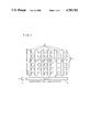
- FIG. 1 is a plane view showing a first embodiment of a solid state image sensing device of the present invention.
- FIGS. 2 is a timings chart showing timing of signals in the first embodiment of FIG. 1, wherein FIG. 2(a) is a composite blanking signal, FIG. 2(b) is a transferring signal for transferring signal charge photoelectrically converted in plural photoelectric conversion devices to vertical transferring means, FIG. 2(c) is a vertical transferring signal, FIG. 2(d) is a horizontal transferring signal, and FIG. 2(e) is an output signal.
- FIG. 3 is a plane view showing a second embodiment of the solid state image sensing device of the present invention.
- FIG. 4 is a timings chart showing timing of signals in the second embodiment of FIG. 3, wherein FIG. 4(a) is a composite blanking signal, FIG. 4(b) is a transferring signal for transferring signal charge photoelectrically converted in plural photoelectric conversion devices to vertical transferring means, FIG. 4(c) is a vertical transferring signal, FIG. 4(d) is a horizontal transferring signal, and FIG. 4(e) is an output signal.
- FIG. 5 is a plane view showing a third embodiment of the solid state image sensing device of the present invention.
- FIG. 6 is a timing chart showing timings of signals in the third embodiment of FIG. 5, wherein FIG. 6(a) is a composite blanking signal, FIG. 6(b) is a transferring signal for transferring signal charge photoelectrically converted in plural photoelectric conversion devices to vertical transferring means, FIGS. 6(c) is a vertical transferring signal, FIG. 6(d) is a horizontal transferring signal, and FIG. 6(e) is an output signal.
- the present invention is described as follows based on an NTSC type television signal, but the present invention is also suitable for a PAL or SECAM type television signal as well.
- the present invention is based on the concept that the blur of an image of a video camera using a solid state image sensing device can be prevented by decreasing the photoelectric conversion period, which effectively corresponds to the control of the shutter speed of the silver salt photography type camera with respect to blurring so that it is shorter than the conventional 1/60 sec.
- electronic shutter is used for representing the above-mentioned electronic controlling.
- a first embodiment of the solid state image sensing device and the method for driving the device of the present invention is described as follows referring to the figures.
- the fundamental constitution of the solid state image sensing device of the first embodiment comprises photoelectric conversion devices 1, vertical transferring means 2 connected to the photoelectric conversion devices 1, a horizontal transferring means 3 connected to the vertical transferring means 2, and signal detecting means 4 connected to the horizontal transferring means 3.
- the arrow marks represent the direction of normal transferring of signal charges.
- FIG. 2 is a timing chart showing typical driving pulses and output signals of the solid state image sensing device of FIG. 1 when the electronic shutter operates.
- FIG. 2(a) shows a composite blanking signal
- FIG. 2(b) shows transferring pulses (hereinafter abbreviated as charge pulses) for transferring signal charges of the photoelectric conversion device 1 to the vertical transferring means 2.
- FIG. 2(c) shows transferring pulses (hereinafter abbreviated as vertical transferring pulses) for transferring signal charges of the vertical transferring means 2 to the horizontal transferring means 3, and FIG.
- FIG. 2(d) shows transferring pulses (hereinafter abbreviated as horizontal transferring pulses and illustrated in a manner such that the illustrated pulse number is less than the real pulse number since the horizontal transferring pulses are extremely high frequency pulses) for transferring signal charges of the horizontal transferring means 3 to the signal detecting means 4.
- FIG. 2(e) shows the output signal from the signal detecting means 4.
- signals which are charged at a photoelectric conversion device 1 in a period 14 and are not to be used for video signals (hereinafter abbreviated as unnecessary signal charge) are transferred to the vertical transferring means 2 by a first charge pulse 11.
- the vertical transferring means 2 transfers the unnecessary signal charges in the vertical transferring means 2 to the horizontal transferring means 3 within a period 13. Therefore, the vertical transferring pulses in a period 15 for transferring the unnecessary signal charges can be generated at a higher speed than normal speed.
- the transferred unnecessary signal charges in the horizontal transferring means 3 are issued by the horizontal transferring means 3 through the signal detecting means 4.
- signal charges which are charged at the photoelectric conversion device 1 in a period 13 after the first charge pulse 11 and which are to be used for the video signal are transferred to the vertical transferring means 2 by a second charge pulse 12.
- signal charges for 1 horizontal line are sequentially transferred to the horizontal transferring means 3 from the vertical transferring means 2 by the vertical transferring pulse in every 1 horizontal period as in the conventional case which does not use the electronic shutter.
- video signals are issued in series from the horizontal transferring means 3 by the horozontal transferring pulse through the signal detecting means 4.
- the signals issued from the solid state image sensing device during the vertical scanning period are only the signal charges which are photoelectrically-converted in the period 13 of FIG. 2. That is, the period 13 is 1/10 to 1/20 in comparison with one field period (1/60 sec). This period thus corresponds to 1/600 to 1/1200 sec shutter speed of the silver salt photography type camera.
- the electronic shutter in this manner, the blur of the image of the moving object can be reduced in the still picture mode, the frame sending mode and the slow picture mode in VTR reproducing.
- the second embodiment intends to resolve the disadvantages mentioned below of the first embodiment. That is, the unnecessary signal charges which are photoelectrically-converted in the period 14 are transferred to the vertical transferring means 2 at the reception of the first charge pulse 11, and are transferred to the horizontal transferring means 3 at the reception of the high-speed vertical transferring pulses, before being further transferred to the signal detecting means 4 and thereby issued as shown in FIG. 2(e). Therefore, in a period 16 when the unnecessary signal charges are issued (FIG. 2(e)) from the signal detecting means 4, the signal charges which have been charged at the photoelectric conversion device 1 in the period 14 are concentratively issued. That is, in the conventional image sensing device, the signal charges charged at the photoelectric conversion device 1 in the period 14 are transferred to the horizontal transferring means 3 in the next vertical scanning period together with the signal charges charged at the photoelectric conversion device 1 in the period 13.
- the signal charges charged at the photoelectric conversion device 1 in the period 14 are concentratively transferred to the horizontal transferring means 3 by the electronic shutter in the next period 15. That is, contrary to conventional transferring of the signal charges which are transferred to the horizontal transferring means 3 in about 250 horizontal periods in the conventional device, the transferring to the horizontal transferring means 3 of the first embodiment of the present device is made within only several horizontal periods. Therefore, the amount of the signal charges is likely to exceed a limit of signal charge amount which can be dealt with by the horizontal transferring means 3 and the signal detecting means 4. Thus, in a period 16 (FIG.
- the second embodiment is described as follows.
- FIG. 3 shows the constitution of the solid state image sensing device of the second embodiment of the present invention.
- the parts 1 to 4 in FIG. 3 correspond to the parts 1-4 in FIG. 1, respectively.
- throw-away means 5 is connected to an end part opposite the horizontal transferring means side of the vertical transferring part 2.
- the arrow indications represent the transferring direction of the normal signal charges (necessary signal charges).
- An interline transfer CCD having 420 (horizontal) ⁇ 490 (vertical) elements is used as the solid state image sensing device.
- FIG. 4 shows the driving pulses and the output signals in the second embodiment.
- FIG. 4(a) shows the composite blanking signal
- FIG. 4(b) shows the charge pulses
- FIG. 4(c) shows the vertical transferring pulses
- FIG. 4(d) shows the horizontal transferring pulses (the illustrated pulse numbers are illustrated as in FIG. 2).
- FIG. 4(e) shows the output signal from the solid state image sensing device of FIG. 3.
- the unnecessary signal charges which have been accumulated in the period 14 are transferred to the vertical transferring means 2 by the first charge pulse 11. Then, in the period 13, the vertical transferring means 2 is driven in a direction contrary to the illustrated arrow direction of FIG. 3 at the issuance of pulses for inverse direction, and thereby all signal charges in the vertical transferring means 2 are transferred to the throw-away means 5. The transferred signal charges are thrown away in the throw-away means 5.
- the throw-away means 5 comprises, for example, an FET and an electric source.
- the signal charges charged in the photoelectric conversion device 1 in the period 13 after the first charge pulse 11 are transferred to the vertical transferring means 2 at issuance of a second charge pulse 12.
- signal charges for 1 horizontal line are sequentially transferred to the horizontal transferring means 3 from the vertical transferring means 2 at issuance of the vertical transferring pulses in every 1 horizontal period, as in the conventional case not using the electronic shutter.
- the signal charges are transferred to the signal detecting means 4 by the horizontal transferring pulses and are issued.
- the unnecessary signal is not issued from the signal detecting means 4.
- FIG. 5 is a third embodiment of the present invention.
- the parts 1 to 4 in FIG. 5 correspond to the parts 1 to 4 in FIG. 1, respectively.
- throw-away means 6 is connected to an end part, opposite the signal detecting means side, of the horizontal transferring means 3.
- the arrow indications represent a normal transferring direction of the signal charges.
- An interline transfer CCD having 420 (horizontal) ⁇ 490 (vertical) elements is used as the solid state image sensing device.
- FIG. 6 shows the driving pulses and the outputs.
- FIG. 6(a) shows the composite blanking signal
- FIG. 6(b) shows the charge pulses.
- FIG. 6(c) shows the vertical transferring pulses
- FIG. 6(d) shows the horizontal transferring pulses (the illustrated pulse number is illustrated as in FIG. 4).
- FIG. 6(e) shows the signal output from the solid state image sensing device.
- the unnecessary signal charges charged till then at the photoelectric conversion device 1 in the period 14 are transferred at issuance of the first charge pulse 11 to the vertical transferring means 2.
- all signal charges in the vertical transferring means 2 are transferred to the horizontal transferring means 3 in the period 13.
- the signal charges are transferred to the throw-away means 6 in a contrary direction (namely, an inverse direction to the illustrated arrow in FIG. 5) to the signal detecting means side by the horizontal transferring means 3 at issuance of pulses for inverse direction.
- the throw-away means 6 throws away all signal charges.
- the throw-away means comprises, for example, an FET and an electric source.
- the signal charges charged at the photoelectric conversion device 1 in the period 13 after the first charge pulse 11 are transferred to the vertical transferring means 2 by a second charge pulse 12.
- signal charges for 1 horizontal line are sequentially transferred to the horizontal transferring means 3 from the vertical transferring means 2 by the vertical transferring pulse in every 1 horizontal period as in the conventional case not using the electronic shutter.
- the signal charges are transferred to the signal detecting means 4 by the horizontal transferring pulses, thereby to be issued.
- the unnecessary signal charges are not issued in the period 19 of FIG. 6(e) from the solid state image sensing device.
- a voltage which is thirty times as large as the normal voltage, caused by the unnecessary signal charges, is not produced at the signal detecting means 4. Further, the large voltage is not produced at a beginning part of the vertical transferring period.
- the second and third embodiments can be combined.
- a frame transfer CCD can be used as the solid state image sensing device.
- the period of the electronic shutter can be freely adjusted by varying the period between the first charge pulse and the second charge pulse.
Abstract
Description
Claims (8)
Applications Claiming Priority (2)
| Application Number | Priority Date | Filing Date | Title |
|---|---|---|---|
| JP60-236062 | 1985-10-22 | ||
| JP60236062A JP2526205B2 (en) | 1985-10-22 | 1985-10-22 | Driving method for solid-state imaging device |
Publications (1)
| Publication Number | Publication Date |
|---|---|
| US4783702A true US4783702A (en) | 1988-11-08 |
Family
ID=16995162
Family Applications (1)
| Application Number | Title | Priority Date | Filing Date |
|---|---|---|---|
| US06/921,493 Expired - Lifetime US4783702A (en) | 1985-10-22 | 1986-10-22 | Method of throwing away unnecessary signal charges in solid state image sensing device |
Country Status (2)
| Country | Link |
|---|---|
| US (1) | US4783702A (en) |
| JP (1) | JP2526205B2 (en) |
Cited By (20)
| Publication number | Priority date | Publication date | Assignee | Title |
|---|---|---|---|---|
| US4856033A (en) * | 1987-03-06 | 1989-08-08 | Sony Corporation | Solid state imager device with exposure control with noise reduction |
| US4858020A (en) * | 1987-01-28 | 1989-08-15 | Canon Kabushiki Kaisha | Image sensing device |
| US4860326A (en) * | 1987-11-10 | 1989-08-22 | Fuji Photo Film Co., Ltd. | Solid-state image pickup device |
| US4862487A (en) * | 1987-04-08 | 1989-08-29 | Hitachi, Ltd. | Solid-state imaging device |
| EP0356034A2 (en) * | 1988-08-24 | 1990-02-28 | Rosemount Limited | Optical sensor |
| US4908709A (en) * | 1987-12-11 | 1990-03-13 | Fuji Photo Film Co., Ltd. | Solid-state electronic imaging device with a photometry function responsive to discarded charge packets |
| GB2226735A (en) * | 1988-12-15 | 1990-07-04 | Asahi Optical Co Ltd | Variable exposure image CCD sensor |
| US4980769A (en) * | 1987-12-25 | 1990-12-25 | Fuji Photo Film Co., Ltd. | Solid-state electronic imaging device having a high speed reverse transfer |
| US4989095A (en) * | 1988-06-15 | 1991-01-29 | Nec Corporation | Controlling method for two dimensional charge-coupled device improved in anti-blooming capability |
| US5001556A (en) * | 1987-09-30 | 1991-03-19 | Olympus Optical Co., Ltd. | Endoscope apparatus for processing a picture image of an object based on a selected wavelength range |
| US5053873A (en) * | 1988-10-11 | 1991-10-01 | Nec Corporation | Solid state image pickup device capable of picking up an image with a long time exposure at a low noise |
| US5113245A (en) * | 1989-10-06 | 1992-05-12 | Fuji Photo Film Co., Ltd. | Image pickup apparatus and method for reducing smear |
| US5121214A (en) * | 1990-06-29 | 1992-06-09 | The United States Of America As Represented By The United States Department Of Energy | Method for eliminating artifacts in CCD imagers |
| US5140426A (en) * | 1989-10-04 | 1992-08-18 | Fuji Photo Film Co., Ltd. | Image pickup device with mechanical shutter for preventing smear |
| US5282041A (en) * | 1988-12-15 | 1994-01-25 | Asahi Kogaku Kogyo Kabushiki Kaisha | Apparatus for driving image pick-up device |
| US5339162A (en) * | 1989-08-08 | 1994-08-16 | Asahi Kogaku Kogyo Kabushiki Kaisha | Driving apparatus of image pick-up device for preventing leakage of accumulated electrical charges |
| US5396286A (en) * | 1992-06-09 | 1995-03-07 | Sony Corporation | Video signal processing apparatus |
| US6429898B1 (en) | 1997-02-26 | 2002-08-06 | Nikon Corporation | Solid state imaging devices and driving methods that produce image signals having wide dynamic range and multiple grey scales |
| US6686962B1 (en) * | 1998-09-28 | 2004-02-03 | Victor Company Of Japan, Limited | Imaging apparatus that reads out an electrical charge from a part of its plurality of photoelectrical conversion elements |
| US20050099512A1 (en) * | 1998-05-28 | 2005-05-12 | Sanyo Electric Co., Ltd. | Digital camera |
Families Citing this family (3)
| Publication number | Priority date | Publication date | Assignee | Title |
|---|---|---|---|---|
| JP2592272B2 (en) * | 1987-12-09 | 1997-03-19 | 富士写真フイルム株式会社 | Color solid-state imaging device |
| JP3141997B2 (en) * | 1988-05-31 | 2001-03-07 | オリンパス光学工業株式会社 | Exposure control method |
| JPH0316478A (en) * | 1989-06-14 | 1991-01-24 | Matsushita Electron Corp | Driving method for solid-state image pickup device |
Citations (4)
| Publication number | Priority date | Publication date | Assignee | Title |
|---|---|---|---|---|
| US3931463A (en) * | 1974-07-23 | 1976-01-06 | Rca Corporation | Scene brightness compensation system with charge transfer imager |
| US4322753A (en) * | 1979-06-08 | 1982-03-30 | Nippon Electric Co., Ltd. | Smear and/or blooming in a solid state charge transfer image pickup device |
| US4584609A (en) * | 1985-04-15 | 1986-04-22 | Rca Corporation | Parallel-input/serial output CCD register with clocking noise cancellation, as for use in solid-state imagers |
| US4651215A (en) * | 1983-05-24 | 1987-03-17 | The General Electric Company, P.L.C. | Image sensors |
Family Cites Families (4)
| Publication number | Priority date | Publication date | Assignee | Title |
|---|---|---|---|---|
| JPS55163882A (en) * | 1979-06-06 | 1980-12-20 | Nec Corp | System for driving charge transfer element |
| JPS5772473A (en) * | 1980-10-22 | 1982-05-06 | Nec Corp | Driving method for charge transfer image pickup device |
| JPS5933979A (en) * | 1982-08-20 | 1984-02-24 | Nippon Kogaku Kk <Nikon> | Driving method of inter-line transfer ccd |
| JPS5980069A (en) * | 1982-10-29 | 1984-05-09 | Toshiba Corp | Image pickup system using solid state image pickup element |
-
1985
- 1985-10-22 JP JP60236062A patent/JP2526205B2/en not_active Expired - Lifetime
-
1986
- 1986-10-22 US US06/921,493 patent/US4783702A/en not_active Expired - Lifetime
Patent Citations (4)
| Publication number | Priority date | Publication date | Assignee | Title |
|---|---|---|---|---|
| US3931463A (en) * | 1974-07-23 | 1976-01-06 | Rca Corporation | Scene brightness compensation system with charge transfer imager |
| US4322753A (en) * | 1979-06-08 | 1982-03-30 | Nippon Electric Co., Ltd. | Smear and/or blooming in a solid state charge transfer image pickup device |
| US4651215A (en) * | 1983-05-24 | 1987-03-17 | The General Electric Company, P.L.C. | Image sensors |
| US4584609A (en) * | 1985-04-15 | 1986-04-22 | Rca Corporation | Parallel-input/serial output CCD register with clocking noise cancellation, as for use in solid-state imagers |
Cited By (27)
| Publication number | Priority date | Publication date | Assignee | Title |
|---|---|---|---|---|
| US4858020A (en) * | 1987-01-28 | 1989-08-15 | Canon Kabushiki Kaisha | Image sensing device |
| US4856033A (en) * | 1987-03-06 | 1989-08-08 | Sony Corporation | Solid state imager device with exposure control with noise reduction |
| US4862487A (en) * | 1987-04-08 | 1989-08-29 | Hitachi, Ltd. | Solid-state imaging device |
| US5001556A (en) * | 1987-09-30 | 1991-03-19 | Olympus Optical Co., Ltd. | Endoscope apparatus for processing a picture image of an object based on a selected wavelength range |
| US4860326A (en) * | 1987-11-10 | 1989-08-22 | Fuji Photo Film Co., Ltd. | Solid-state image pickup device |
| US4908709A (en) * | 1987-12-11 | 1990-03-13 | Fuji Photo Film Co., Ltd. | Solid-state electronic imaging device with a photometry function responsive to discarded charge packets |
| US4980769A (en) * | 1987-12-25 | 1990-12-25 | Fuji Photo Film Co., Ltd. | Solid-state electronic imaging device having a high speed reverse transfer |
| US4989095A (en) * | 1988-06-15 | 1991-01-29 | Nec Corporation | Controlling method for two dimensional charge-coupled device improved in anti-blooming capability |
| EP0356034A2 (en) * | 1988-08-24 | 1990-02-28 | Rosemount Limited | Optical sensor |
| EP0356034A3 (en) * | 1988-08-24 | 1990-07-25 | Rosemount Limited | Optical sensor |
| US4987294A (en) * | 1988-08-24 | 1991-01-22 | Rosemount Limited | Optical sensor with plual detectors and pulse sandwiching |
| US5053873A (en) * | 1988-10-11 | 1991-10-01 | Nec Corporation | Solid state image pickup device capable of picking up an image with a long time exposure at a low noise |
| GB2226735A (en) * | 1988-12-15 | 1990-07-04 | Asahi Optical Co Ltd | Variable exposure image CCD sensor |
| GB2226735B (en) * | 1988-12-15 | 1993-12-15 | Asahi Optical Co Ltd | Apparatus for driving image pick-up device |
| US5282041A (en) * | 1988-12-15 | 1994-01-25 | Asahi Kogaku Kogyo Kabushiki Kaisha | Apparatus for driving image pick-up device |
| US5416517A (en) * | 1988-12-15 | 1995-05-16 | Tani; Nobuhiro | Apparatus for driving image pick-up device including smear prevention |
| USRE36812E (en) * | 1989-08-08 | 2000-08-08 | Asahi Kogaku Kogyo Kabushiki Kaisha | Driving apparatus of image pick-up device for preventing leakage of accumulated electrical charges |
| US5339162A (en) * | 1989-08-08 | 1994-08-16 | Asahi Kogaku Kogyo Kabushiki Kaisha | Driving apparatus of image pick-up device for preventing leakage of accumulated electrical charges |
| US5140426A (en) * | 1989-10-04 | 1992-08-18 | Fuji Photo Film Co., Ltd. | Image pickup device with mechanical shutter for preventing smear |
| US5113245A (en) * | 1989-10-06 | 1992-05-12 | Fuji Photo Film Co., Ltd. | Image pickup apparatus and method for reducing smear |
| US5121214A (en) * | 1990-06-29 | 1992-06-09 | The United States Of America As Represented By The United States Department Of Energy | Method for eliminating artifacts in CCD imagers |
| US5396286A (en) * | 1992-06-09 | 1995-03-07 | Sony Corporation | Video signal processing apparatus |
| US6429898B1 (en) | 1997-02-26 | 2002-08-06 | Nikon Corporation | Solid state imaging devices and driving methods that produce image signals having wide dynamic range and multiple grey scales |
| US20050099512A1 (en) * | 1998-05-28 | 2005-05-12 | Sanyo Electric Co., Ltd. | Digital camera |
| US6897895B1 (en) * | 1998-05-28 | 2005-05-24 | Sanyo Electric Co., Ltd. | Digital camera |
| US7573511B2 (en) | 1998-05-28 | 2009-08-11 | Sanyo Electric Co., Ltd. | Digital camera |
| US6686962B1 (en) * | 1998-09-28 | 2004-02-03 | Victor Company Of Japan, Limited | Imaging apparatus that reads out an electrical charge from a part of its plurality of photoelectrical conversion elements |
Also Published As
| Publication number | Publication date |
|---|---|
| JPS6295077A (en) | 1987-05-01 |
| JP2526205B2 (en) | 1996-08-21 |
Similar Documents
| Publication | Publication Date | Title |
|---|---|---|
| US4783702A (en) | Method of throwing away unnecessary signal charges in solid state image sensing device | |
| US5438365A (en) | Solid-state imaging apparatus employing independently variable odd and even lines of photodiodes | |
| EP1921841B1 (en) | Monitoring method with a CCD imaging device and digital still camera using the same | |
| US5047858A (en) | Multiple image processing and display system | |
| EP0120678B1 (en) | Color solid-state image sensor | |
| US5018006A (en) | Multi-plate type image pickup apparatus having picture elements for producing color and luminance signals | |
| CA1191942A (en) | Solid state image pick-up devices | |
| US4980771A (en) | Imaging device and imaging apparatus including the imaging device | |
| CA2062631A1 (en) | Image sensing apparatus having plurality of optical systems and method of operating such apparatus | |
| US4651227A (en) | Video signal recording apparatus with A/D conversion | |
| EP0596748A2 (en) | CCD imager for obtaining a plurality of aspect ratios, making effective use of the photosensible area | |
| US5006928A (en) | Image processing method in an electronic video endoscopy system | |
| EP0243977B1 (en) | Still image pickup camera | |
| CA2052148A1 (en) | Method of driving a solid-state imaging device | |
| US5576762A (en) | Solid-state image pickup device | |
| EP0087296B1 (en) | Apparatus and method for generating high quality pictures under low light conditions | |
| EP0161752B1 (en) | Image signal reproduction circuit for swing image sensor | |
| GB2151105A (en) | Ccd imager | |
| US4244003A (en) | Charge proportional opto-electronic converter providing enhanced blue color signal | |
| EP0740475B1 (en) | Image pick-up apparatus | |
| KR930009102B1 (en) | Record auto-exchange circuit | |
| JPS58115980A (en) | Driving method for solid-state image pickup element | |
| JP2692219B2 (en) | Solid-state imaging device | |
| KR0174947B1 (en) | Still image recording apparatus using variable speed shutter of camcorder | |
| JPS57164667A (en) | Solid image pickup device |
Legal Events
| Date | Code | Title | Description |
|---|---|---|---|
| AS | Assignment |
Owner name: MATSUSHITA ELECTRONICS CORPORATION, 1006, OAZA-KAD Free format text: ASSIGNMENT OF ASSIGNORS INTEREST.;ASSIGNORS:SONE, YOSHIAKI;KURODA, TAKAO;REEL/FRAME:004652/0121 Effective date: 19861017 Owner name: MATSUSHITA ELECTRONICS CORPORATION, JAPAN Free format text: ASSIGNMENT OF ASSIGNORS INTEREST;ASSIGNORS:SONE, YOSHIAKI;KURODA, TAKAO;REEL/FRAME:004652/0121 Effective date: 19861017 |
|
| STCF | Information on status: patent grant |
Free format text: PATENTED CASE |
|
| FEPP | Fee payment procedure |
Free format text: PAYOR NUMBER ASSIGNED (ORIGINAL EVENT CODE: ASPN); ENTITY STATUS OF PATENT OWNER: LARGE ENTITY |
|
| FPAY | Fee payment |
Year of fee payment: 4 |
|
| FEPP | Fee payment procedure |
Free format text: PAYER NUMBER DE-ASSIGNED (ORIGINAL EVENT CODE: RMPN); ENTITY STATUS OF PATENT OWNER: LARGE ENTITY Free format text: PAYOR NUMBER ASSIGNED (ORIGINAL EVENT CODE: ASPN); ENTITY STATUS OF PATENT OWNER: LARGE ENTITY |
|
| FPAY | Fee payment |
Year of fee payment: 8 |
|
| FPAY | Fee payment |
Year of fee payment: 12 |
|
| AS | Assignment |
Owner name: MATSUSHITA ELECTRIC INDUSTRIAL CO., LTD., JAPAN Free format text: CHANGE OF NAME;ASSIGNOR:MATSUSHITA ELECTRONICS CORPORATION;REEL/FRAME:012495/0898 Effective date: 20010404 |