US4792793A - Converting numbers between binary and another base - Google Patents
Converting numbers between binary and another base Download PDFInfo
- Publication number
- US4792793A US4792793A US07/055,184 US5518487A US4792793A US 4792793 A US4792793 A US 4792793A US 5518487 A US5518487 A US 5518487A US 4792793 A US4792793 A US 4792793A
- Authority
- US
- United States
- Prior art keywords
- register
- convert
- product
- bits
- digits
- Prior art date
- Legal status (The legal status is an assumption and is not a legal conclusion. Google has not performed a legal analysis and makes no representation as to the accuracy of the status listed.)
- Expired - Lifetime
Links
Images
Classifications
-
- H—ELECTRICITY
- H03—ELECTRONIC CIRCUITRY
- H03M—CODING; DECODING; CODE CONVERSION IN GENERAL
- H03M7/00—Conversion of a code where information is represented by a given sequence or number of digits to a code where the same, similar or subset of information is represented by a different sequence or number of digits
- H03M7/02—Conversion to or from weighted codes, i.e. the weight given to a digit depending on the position of the digit within the block or code word
- H03M7/06—Conversion to or from weighted codes, i.e. the weight given to a digit depending on the position of the digit within the block or code word the radix thereof being a positive integer different from two
Definitions
- the invention relates to apparatus for converting numbers bidirectionally between binary and another base, such as binary-coded decimal.
- a number coded according to an arbitrary radix b may be stored in a data processing system as a sequence of nibbles (distinct groups of bits), each nibble containing one radix-b digit.
- each nibble is four bits wide and contains a decimal digit ranging in value between zero and nine.
- a typical algorithm for converting a radix-b number to binary operates by first initializing a binary accumulator to zero and then going into a loop in which the leading digit is peeled off the radix-b number and added into the binary accumulator while the previous contents of the accumulator are concurrently multiplied by b.
- One problem with using this algorithm is that multiplication is usually a two-step process, requiring two cycles to complete. The sum and carrying bits from a carry/save adder (CSA) are generated on the first cycle, and they are added together (and with the leading radix-b digit) on the second cycle. The approach therefore requires two clock cycles for each radix-b digit to complete.
- CSA carry/save adder
- the conversion may be improved to perform in one clock cycle per radix-b digit if two multiply-and-add algorithms are interleaved in the same multiplier. For example, a first accumulation may be made by multiplying the first digit by b 2 and adding the third digit, then multiplying the result by b 2 and adding the fifth digit, etc. The second accumulation may be obtained by multiplying the second digit by b 2 and adding the fourth digit, multiplying the result by b 2 and adding the sixth digit, etc. While one accumulation is in the multiply stage, the other accumulation is in the adding stage. After both accumulations are complete, the appropriate one is multiplied by b and added to the other to obtain the binary result. This technique converts one digit to binary for each clock cycle, but as can be seen, adds significant complexity in control logic.
- the conversion may be performed in two stages.
- the initial multiplication is by 10 -4 to obtain a first product.
- the integer portion of the first product is stored, and the fractional part is used to generate the low-order four digits of the result.
- the high-order six digits are obtained by multiplying the integer portion of the first product by 10 -5 .
- the high-order six digits are then generated as above. This variation speeds up conversion of binary numbers less than 10,000 at the slight expense of conversion of numbers greater than or equal to 10,000.
- both the one-stage version and the two-stage version of this algorithm require the services of a multiplier. Since the result of each multiplication is needed before the next one begins, two clock cycles are required to generate each radix-b digit.
- the above objects and others are accomplished according to the invention by providing dedicated convert hardware as a separate functional unit operating independently from any general purpose multiplier.
- the dedicated convert hardware comprises a special purpose multiply-and-add unit and a convert register.
- the output of the multiply-and-add unit is coupled to the input of the convert register, and the output of the convert register is recycled to the inputs of the multiply-and-add unit.
- the multiply-and-add unit is hardwired to multiply the input by b and concurrently add the value at a separate digit input. Means are also provided for initializing the convert register with zero or with any desired number.
- the convert hardware is operated to convert a number from radix-b to binary by first initializing the convert register to zero and then iteratively clocking the multiply-and-add unit output into the convert register while presenting to the digit input of the multiply-and-add unit successively high- to low-order digits of the radix-b number.
- the convert hardware is operated to convert a binary number to radix-b by first initializing the convert register with the fractional part of a product N*b -m , where N is the binary number and m is an integer greater than zero as described above, and then repetitively clocking the output of the multiply-and-add unit into the convert register while the digit input of the multiply-and-add unit is held at zero.
- the integer part of each successive multiplication constitutes the successive radix-b digits. These may be shifted into a result register immediately, or stored temporarily in unused high-order bits of the convert register. Only the fractional part of each product is recirculated to the multiply-and-add unit, effectively clearing the integer part each cycle.
- the multiply-and-add unit may be a combinational 3-input adder having first, second and third inputs.
- the first input is supplied with a version of the convert register output shifted left by one bit and the second input is supplied with a version of the convert register output shifted left by three bits. Since a one-bit left shift of a binary number is effectively a multiplication by two, and a 3-bit left shift of a binary number is effectively a multiplication by eight, the addition of the first and second input values is effectively a multiplication by 10.
- the connection between the convert register output and the first and second inputs of the adder therefore effectively converts the adder into a dedicated unit for performing high speed multiplication by 10.
- the dedicated multiply-and-add unit of the present invention requires a minimal number of logic levels to implement, and may therefore be made fast enough to operate in one clock cycle. Additionally, it will now be apparent that conversions of numbers between binary and another radix b ⁇ 10 may be performed using similar hardwired connections between the convert register output and inputs of a combinational adder (or subtractor, if appropriate), with left shifts appropriate for the value of b.
- the dedicated convert hardware of the present invention requires only a minimal amount of additional logic, because the same logic is used for conversions in both directions. Algorithms have been chosen for performing the conversions which both employ iterative multiplication by b. For conversions from radix b to binary, the third input of the dedicated multiply-and-add unit is supplied with successive high- to low-order digits of the radix-b number and the absolute value of the resulting binary number is iteratively calculated in the low-order bits of the convert register.
- the fractional part of the b -m product is initialized into the very same convert register, and recycled through the very same multiply-and-add unit to iteratively generate digits of the radix-b number. It can be seen that the dedicated hardware of the present invention and the use of such hardware to perform high speed radix conversions in both directions is a significant advance over the prior art.
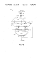
- FIGS. 1-3 show various functional units of a data processing unit in which the invention may be used
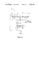
- FIG. 4 shows apparatus which may be used with the apparatus of FIGS. 1-3 to implement the invention for bidirectional conversion between binary and decimal.
- Computer systems based on the IBM System/370 include a CVB instruction to convert a decimal number into binary and a CVD instruction to convert a binary number into decimal.
- the binary numbers for both instructions are 32 bits wide in twos-complement form. They can represent values in the range of -2,147,483,648 to +2,147,483,647.
- the leftmost bit of the binary number is the sign bit. If it is zero, then the binary number is zero or positive and the rightmost 31 bits represent the absolute value of the number. If the sign bit is set, then the number is negative and its asolute value may be obtained by complementing all 32 bits and adding one.
- decimal numbers are stored in 64-bit double words, the high order 60 bits of which contain 15 decimal digits of the absolute value of the number and the low order four bits of which contain a sign code to indicate whether the number is positive or negative.
- a sign code of 1100 indicates that the number is positive and a sign code of 1101 indicates that the number is negative.
- any 32-bit binary number may be converted to the decimal form described above, but a decimal number must be within the range of -2,147,483,648 to +2,147,483,647 to be converted into a 32-bit binary number. Additionally, no 4-bit numeric digit of the decimal number may contain a value greater than 9. If CVB encounters a decimal number with valid digits and sign codes, but with an absolute value larger than that which can be represented by a 32-bit binary number, then a fixed-point divide exception is recognized and only the low-order 32 bits of the binary result are generated. If CVB encounters a decimal number with an invalid digit or sign code, then a data exception is recognized and the execution of the instruction is terminated or suppressed.
- specialized convert hardware which operates as part of a large and powerful computing system, relevant parts of which are shown in FIGS. 1-3.
- the implementation herein described is that used in a fixed point processing unit (FXU).
- FXU fixed point processing unit
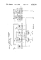
- FIG. 1 six 32-bit registers are shown, labelled OWRH, OWRX, OWRY, OWRL, RRH and RRL.
- Registers OWRH and OWRL receive data from other parts of the computing system for processing by the FXU.
- Registers RRH and RRL hold results from the various functional units in the FXU.
- Registers OWRX and OWRY hold data temporarily; they are not directly connected outside the FXU.
- FIG. 1 Also shown in FIG. 1 are two 32-bit buses labelled OWRHSEL and OWRLSEL.
- Two data selectors 20 and 22 are used to select data onto OWRHSEL and OWRLSEL, respectively. Reading from left to right, the data selector 20 may select any one of the following: a word of all zeros; the output of OWRH; the logical complement of OWRH; the output of OWRX; the output of OWRY; the output of OWRL; or the output of RRH.
- Data selector 22 may select a word of all ones; the output of OWRH; the output of OWRX; the output of OWRY; the output of OWRL; the output of RRL; or a word of all zeros.
- control unit 24 The selection performed by data selectors 20 and 22, as well as that performed by other data selectors to be described, is accomplished according to control signals generated by a control unit 24.
- the control unit 24 may be microcoded or hardwired, and it updates the control signals once every clock cycle.
- Programmed signals may be presented to the control unit 24 from an Instruction Unit, for example, which tells the FXU to perform a given machine level instruction, such as CVB or CVD.
- the frequency at which the control unit 24 updates its control signals output is referred to as the clock cycle time of the FXU.
- the cycle time can be no faster than the longest data path between two latch points in the computer system. Otherwise, the usual practice is either to slow the clock frequency, which degrades the throughput of the entire computer system as previously described, or divide the longest data paths into two or more segments by inserting additional intermediate latch points. For data paths passing through multipliers the latter solution is most often used, with the consequent disadvantages described above.
- Data selector 30 can select any of several inputs, including the output of RRH; the output of RRL; the output of data selector 40; or the output of data selector 38.
- Data selector 32 can select a word of all ones; the true or complement of the output of RRH; the complement of another FXU bus called the L Bus (described below); the output of OWRX; or the true or complement output of OWRL.
- Data selector 34 can select the output of OWRX; the output of OWRY; the output of RRL; or the true or complement of the output of OWRH.
- Data selector 36 can select from several inputs, including RRH; RRL; the output of data selector 40 or the output of data selector 38.
- Data selector 38 can select a 32-bit word from any of the following: a word of all zeros, the output of a general purpose carry propagate adder (CPA) 50 shown in FIG. 2, the L Bus, the high-order 32 bits of the 40-bit output of a general purpose multiplier (MCPA) described below, a 32-bit SHH signal described below, the output of OWRH, the output of RRH, or a composite formed by bits 0-23 of SHH in the high-order 24 bits and bits 24-31 of L Bus in the low-order 8 bits.
- CPA general purpose carry propagate adder
- MCPA general purpose multiplier
- Data selector 40 may select a 32-bit word from any of the following: a word of all zeros, CPA, L Bus, the output of an SHL register described below, OWRL, RRL or a composite formed by bits 32-39 of the 40-bit MCPA signal in the high-order 8 bits and bits 8-31 of SHL in the low-order 24 bits.
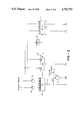
- FIG. 2 several of the functional units of the FXU which are used in the radix conversion algorithms are shown. They include a 64-bit divide register (DR) 52, the previously mentioned carry propagate adder 50 and a 64-bit shifter 54.
- the divide register 52 is part of a fixed-point division functional unit, not shown, which is not otherwise important to the present invention.
- the inputs to DR 52 are selected in two 32-bit portions, the high-order 32 bits being selected by a data selector 56 and the low-order portion being selected by data selector 58. Both data selectors 56 and 58 are controlled by the same set of control signals (not shown).
- the data selector 56 selects data from either the OWRHSEL bus or another source (not shown).
- the data selector 58 selects data from either the OWRLSEL bus or another source (not shown).
- the other sources (not shown) for data selectors 56 and 58 are not used with the present invention.
- CPA 50 is a 32-bit adder, capable of adding two 32-bit numbers CPA1 and CPA2.
- CPA1 is connected to OWRHSEL and CPA2 is connected to OWRLSEL.
- the output of CPA 50 is connected to the data selectors 38 and 40 (FIG. 1) as previously described.
- CPA 50 also has a carry input CI and carry output CO.
- the shifter 54 shifts 64 bits of data from OWRHSEL and OWRLSEL by up to 63 bits in either direction.
- the shift amount and direction is loaded in the previous cycle into a Shift Amount Register (SAR) 60.
- SAR Shift Amount Register
- the high-order 32 bits of the output of shifter 54 go to SHH, and the low-order 32 bits of shifter 54 go to SHL.
- SHH may be selected into RRH and SHL may be selected into RRL.
- Shifts may be logical or arithmetic, but only logical shifts are used in the present embodiment.
- a data selector 70 which selects a 32-bit word for the L Bus.
- the data may be selected from the high-order 32 bits of DR register 52; the low-order 32 bits of of a 39-bit CVR convert register 110 (shown in FIG. 4) described below; or a word made up of the high-order 8 bits of CVR register 110 in the low-order 8 bits and zeros in the high-order 24 bits.
- Other sources may also be selected onto the L Bus.
- FIG. 3 there is shown a general purpose binary multiplier 80 which forms another functional unit of the FXU.
- the multiplier 80 is capable of multiplying a 32-bit binary number by an 8-bit multiplicand, but contains data paths such that larger multiplicands may be used if iterative multiplication is acceptable.
- the multiplier 80 consists of an 8-bit IER register 82 for holding the smaller multiplicand, into which may be selected (by a data selector 84) the low-order 8 bits of SHL, the hex numbers 4C or 37, or another number supplied as a literal from the control means 24.
- the output of IER register 82 is connected to one input of a carry save adder (CSA) 86, the other input of which is connected to the high-order 32 bits of DR.
- CSA carry save adder
- the CSA 86 generates a partial sum (PS) and a partial carry (PC), each 40 bits wide, which are coupled respectively to first and second inputs of another CSA 88.
- CSA 88 also has a third 40-bit input, the high-order eight bits of which are supplied with all zeros, and the low-order 32 bits of which are connected as described below.
- CSA 88 generates a 40-bit MULT SUM and a 40-bit MULT CARRY signal. These are coupled to respective data selectors 90 and 92, the outputs of which are connected to the inputs of, respectively, a sum register (SR) 94 and a carry register (CR) 96.
- the data selectors 90 and 92 can also each select a 40-bit word of all zeros.
- SR register 94 and CR register 96 are added together by a multiplier carry propagate adder (MCPA) 98.
- MCPA multiplier carry propagate adder
- the high-order 32 bits of the output of MCPA 98 recirculate and supply the low-order 32 bits of the third input of CSA 88.
- the high-order 32 bits of the 40-bit MCPA output is selectable into RRH, and the low-order 8 bits of the 40-bit MCPA output is selectable into RRL.
- the first operand is loaded into the leftmost 32 bits of DR and the low-order eight bits of the other operand are loaded into IER register 82. Zeros are loaded into SR register 94 and CR register 96.
- the output of CSA 88 is loaded into SR register 94 and CR register 96; the next eight bits of the second operand are loaded into IER register 82; whatever was previously in RRL is shifted right by eight bits; and bits 32-39 of MCPA are loaded into bits 0-7 of RRL.
- RRL is shifted right by 8 bits; bits 32-39 of MCPA are loaded into bits 0-7 of RRL; and bits 0-31 of MCPA are loaded into RRH.
- FIG. 4 there is shown specialized convert hardware 102 according to the invention for bidirectionally converting numbers between binary and decimal. It consists of a three-input carry propagate adder (CVCPA) 104, a convert register (CVR) 110, and two data selectors 112 and 114.
- the three inputs of CVCPA 104 (CVCPA1, CVCPA2 and CVCPA3) are each 35 bits wide. The first and second of these are connected as described below.
- the third input of CVCPA 104 has its low-order four bits connected to the high-order four bits of RRH. The high-order 31 bits of the input are provided with all zeros.
- the 35-bit output of CVCPA 104 is coupled to the data selector 114, the output of which is connected to the low-order 35 bits of CVR register 110.
- Data selector 114 may also select a 35-bit word consisting of zeros in bits 0-3 (appearing in bits 4-7 of CVR), the low-order 28 bits of RRH in bits 4-31 (appearing in bits 8-35 of CVR) and zeros in bits 32-34 (appearing in bits 36-38 of CVR).
- CVR register 110 is a 39-bit register, the output of which may be coupled to the L Bus as previously described by data selector 70 (FIG. 2). Additionally, the low-order 31 bits of CVR are recirculated and connected to the first and second inputs of CVCPA 104. The connection to CVCPA1 is shifted left by one bit, such that CVR bit 38 is connected to CVCPA1 bit 33; CVR bit 37 is connected to CVCPA1 bit 32; and so on until CVR bit 8 is connected to CVCPA1 bit 3. CVCPA1 bits 34 and 0-2 are held at 0. In effect, therefore, the value at the CVCPA1 input is equal to two times the value in CVR bits 8-38.
- CVCPA2 is equal to 8 times the value in CVR bits 8-38. Since CVCPA adds twice the value in CVR(8:38) to 8 times the value in CVR(8:38), CVCPA 104 effectively generates 10 times CVR(8:38) (plus the value at CVCPA3) in a fast, hardwired, combinational manner. It can be seen that if b is different from 10, another hardwired configuration such as this may be used to generate b times CVR(8:38).
- CVR bits 4-7 are connected through a four-bit data selector 112 to the CVR inputs for bits 0-3.
- Data selector 112 can also select four bits of zeros to present to the inputs for CVR bits 0-3. It will be shown below that CVR register 110 is wider than absolutely necessary to perform conversions, since only the low-order 32 bits are used in conversions to binary, and though all of the 32 low-order bits are used to perform conversions to decimal, only bits 8-29 are necessary.
- the high-order eight bits of CVR register 110 are used only for temporarily storing pairs of BCD digits as they are generated by the convert hardware 102.
- the decimal result would consist of five leading zero digits followed by one digit obtained from the integer part of the product, followed by nine digits obtained from computations on the fractional part of the product.
- the computations on the fractional part consist of a loop in which each iteration multiplies the fraction by 10.
- the integer part of the product from each of these iterative multiplications forms another digit of the decimal number, and the fractional part is used by the next iteration of the loop.
- the conversion process is divided into two stages in the belief that most numbers which are converted are relatively small.
- This procedure speeds up the conversion for numbers with an absolute value of less than 1000, but it makes the conversion of larger numbers a little slower.
- the binary number is multiplied by 10 -3 to obtain a first product. If the integer part of the first product is zero, then the procedure for numbers less than 1000 is followed: three decimal digits are generated from the fractional part by iterative multiplication by 10; twelve leading zero digits are appended to the left; and the sign code is appended to the right. If the integer part of the first product is not zero, then the procedure for numbers greater than or equal to 1000 is followed.
- Three decimal digits are generated from the fractional part of the first product by iterative multiplication by 10, and the sign is appended to the right; these three digits and sign are saved left justified in OWRX.
- the integer part of the first product is then multiplied by 10 -6 producing a second product with a second integer part and a second fractional part.
- the new integer part has a value of at most two.
- Six decimal digits are generated from the second fractional part by iterative multiplication by 10.
- the final result consists of 5 leading zero digits, followed by the second integer part (1 digit), followed by the 6 digits generated from the second fractional part, followed by the 3 digits generated from the fraction part of the first product, followed by the sign code.
- the number used to represent 10 -3 in base 16 notation is ⁇ 0.004189374C ⁇ . Actually, this number is slightly larger than 10 -3 (and ⁇ 0.004189374B ⁇ is slightly smaller than 10 -3 ).
- the number used to represent 10 -6 in base 16 notation is ⁇ 0.000010C6F8 ⁇ . Actually this number is slightly larger than 10 -6 (and ⁇ 0.000010C6F7 ⁇ is slightly smaller than 10 -6 ). Since both of the numbers used are slightly larger than the values that they represent, small errors are introduced into the calculation. Furthermore, the fractional parts of the products so computed are rounded up to the next value that fits into 28 bits, thereby introducing additional small errors. Appendix III shows, however, that these errors have no effect on the accuracy of the result.
- CVR register 100 On the high-order end of CVR register 100, the low-order four bits of the integer part of the multiplication by 10 -6 and of the iterative multiplications are placed in CVR(4:7). That information is shifted over to CVR(0:3) each cycle to make room for the integer portion of a new product.
- CVR(0:7) actually be part of the same register as CVR(8:38): the low-order four bits of the integer portion of the 10 -6 multiplication result contain the first decimal digit, which may instead be stored elsewhere since no further processing of such digit is required; and the low-order four bits of the integer portion of each iteration multiplication contains a different decimal digit which also needs no further processing and which may likewise be stored elsewhere or immediately shifted into a result register.
- CVR(4:7) is also used to detect data overflow in CVB, but this function may be performed at the output of CVCPA 104.
- the use of temporary storage means appended to the high-order end of CVR register 110 is merely a convenient way, given the architecture and data paths of the FXU, for temporarily storing the above information.
Abstract
Description
APPENDIX I ______________________________________ CONVERSION FROM DECIMAL TO BINARY COPYRIGHT 1986 AMDAHL CORPORATION ______________________________________ Setup Load decimal operand into OWRH and OWRL with the most significant digits in OWRH First Cycle OWRH → OWRY OWRL → OWRX OWRH → OWRHSEL OWRL → OWRLSEL Number of leading zero digits in OWRSEL → COUNTER1 "LEFT (4 times number of leading zero digits)" →SAR 0 → RRH (will be used to clear CVR on next cycle) 0 →RRL 0 → OVERFLOW --TRIGGER If all digits (except sign digit) in OWRSEL are zero, then set ZERO --TRIGGER (operand is zero) otherwise, reset ZERO --TRIGGER (operand is nonzero) Second Cycle OWRY → OWRHSEL OWRX → OWRLSEL Execute logical shift to eliminate leading zero digits SHH → RRH SHL → RRL (Significant digits are now left justified in RRH/RRL) COUNTER1 -15 → COUNTER1 (to put number of significant digits into COUNTER1) 0 → CVR<0:7>; RRH<4:31> → CVR<8:35>; 0 → CVR<36:38> (Clear CVR. ZERO was put in RRH in previous cycle) "LEFT 4" → SAR (for moving next decimal digit into place in the next cycle) Hold OVERFLOW --TRIGGER Decode decimal sign code from OWRLSEL<28:31> If sign code is negative, then set SIGN1 --TRIGGER If sign code is positive, then reset SIGN1 --TRIGGER If ZERO --TRIGGER is set, then branch to "Next to Last Cycle (Zero Result)" Loopinq Cycle CVR shifted left 1 bit → CVCPA1 CVR shifted left 3 bits → CVCPA2 RRH<0:3> → CVCPA3 (right justified) CVCPA → CVR<4:31> (CVCPA is 10*CVR<8:38> + RRH<0:3>) CVR<4:7> → CVR<0:3> (happens automatically each clock cycle but makes no difference for conversion to binary) RRH → OWRHSEL RRL → OWRLSEL Execute logical shift to move next decimal digit into place "LEFT 4" → SAR (to prepare for logical shift on next repetition of this cycle) If CVR<4:7> = 0 then set OVERFLOW --TRIGGER else hold OVERFLOW -- TRIGGER (CVR<4:7> will be nonzero only if original decimal number was too large) Hold SIGN1 --TRIGGER Decrement COUNTER1 If COUNTER1 (before the decrement) > 1, repeat this cycle Next to Last Cycle (Nonzero Result) CVR<7:38> → L --BUS (through data selector 70 (FIG. 2)) L --BUS → RRH L --BUS → OWRX (prepare to complement and add 1 if result was negative) If CVR<4:6> = 0, then set OVERFLOW --TRIGGER If (CVR<7> = 0 and CVR<8:38> =0), then set OVERFLOW --TRIGGER If (CVR<7> = 0) and SIGN1 --TRIGGER is not set) then set OVERFLOW --TRIGGER If OVERFLOW --TRIGGER is already set, then leave it set If SIGN1 --TRIGGER is set, then branch to "Last Cycle (Negative Result)" else branch to "Last Cycle (Positive Result)" Notify other units of computer that execution of this instruction is almost finished Last Cycle (Positive Result) Hold RRH OVERFLOW --TRIGGER → FIXED --POINT --DIVIDE --INTERRUPT Last Cycle (Negative Result) OWRX → OWRHSEL 0 → OWRLSEL 1 → CPA --CARRY --IN CPA → RRH OVERFLOW --TRIGGER → FIXED --POINT --DIVIDE --INTERRUPT Next to Last Cycle (Zero Result) Notify other units of computer that execution of this instruction is almost finished Last Cycle (Zero Result) 0 → RRH ______________________________________
APPENDIX II ______________________________________ CONVERSION FROM BINARY TO DECIMAL COPYRIGHT 1986 AMDAHL CORPORATION ______________________________________ Setup Load binary operand into OWRL Cycle 1 OWRL → OWRX (Need this if operand negative) OWRL → OWRHSEL OWRHSEL → DR<0:31> (DR<0:31> contains one operand for binary multiplier 80) `4C`X → IER (Low-order byte of 10.sup.-3 becomes other operand for binary multiplier 80) 0 →SR 0 → CR If OWRHSEL=0 then set ZERO --TRIGGER else reset ZERO --TRIGGER If OWRHSEL<0> is set, then branch to Cycle 50 (operand is negative) Note: Cycles 2-6 do setup work for positive operands, including multiplication by 10.sup.-3 and building the positive sign code. Cycles 50-56 do setup work for negative operands, including calculating the absolute value of the operand, multiplication by 10.sup.-3 and building the negative sign code.
Cycle 2
ONES → OWRX (Need this if operand zero)
MULTIPLY --SUM → SR
MULTIPLY --CARRY → CR
`37`X →  IER (Next byte of 10.sup.-3)
DR → DR
"LEFT 30" → SAR
If ZERO --TRIGGER is set, then branch to Cycle 90
 (operand was zero)
Cycle 3
OWRX → OWRHSEL
Shift left 30 bits (to build positive sign code)
SHH → RRH (Positive sign code → RRH<0:3>)
MCPA<32:39> → RRL<0:7> (Low-order 8 bits of product)
MULTIPLY --SUM → SR
MULTIPLY --CARRY → CR
`89`X → IER (next byte of 10.sup.-3)
DR → DR
"RIGHT 8" → SAR
Cycle 4
RRH → OWRX (Positive sign code → OWRX<0:3>)
RRL → OWRLSEL
Shift completed part of product right 8 bits
SHL<8:31> → RRL<8:31>
MCPA<32:39> → RRL<0:7>
MULTIPLY --SUM → SR
MULTIPLY --CARRY → CR
`41`X → IER (next byte of 10.sup.-3)
DR → DR
"RIGHT 8" → SAR
Cycle 5
OWRX →  OWRX (Positive sign code in OWRX<0:3>)
RRL → OWRLSEL
Shift completed part of product right 8 bits
SHL<8:31> → RRL<8:31>
MCPA<32:39> → RRL<0:7>
MULTIPLY --SUM → SR
MULTIPLY --CARRY → CR
`41`X → IER (next byte of 10.sup.-3)
"RIGHT 8" → SAR
Cycle 6
OWRX → OWRX (Positive sign code in OWRX<0:3>)
RRL → OWRLSEL
Shift completed part of product right 8 bits
SHL<8:31> → RRL<8:31>
MCPA<32:39> → RRL<0:7>
MCPA<0:31> → RRH
"LEFT 20" → SAR
 (Integer part of product is in RRH<0:23>)
 (Fractional part of product is in RRH<24:31> and
  RRL, but only RRH<24:31> and RRL<0:19> will
  be used)
 Note:
 Cycles 7-11 are shared by the <1000 case and the ≧ 1000 case.
Cycle 7
OWRX → OWRY (Sign code → OWRY<0:3>)
RRH → OWRX (Integer part of 10.sup. -3 Product →
 OWRX<0:23> for safekeeping)
RRH → OWRHSEL
RRL → OWRLSEL
Shift left 20 bits (puts fractional part in RRH<4:31>)
SHH → RRH
Cycle 8
RRH → OWRHSEL
0 → OWRLSEL
1 → CPA --CARRY --IN
CPA → RRH (Increment fractional part to make up for
 truncation)
OWRX → OWRX (holding integer part of 10.sup.-3 product)
OWRY → OWRY (Sign code in OWRY<0:3>)
"RIGHT 8" → SAR
Cycle 9
0 → CVR<0:7,36:38>
RRH<4:31> → CVR<8:35>
OWRY → OWRY (Sign code in OWRY<0:3>)
OWRX → OWRHSEL
Shift integer part right 8 bits to right justify it in
 RRH
SHH → RRH (Also ensures that RRH<0:3> are zero for
 next cycle)
If SHH = 0, then set ZERO --TRIGGER else reset
 ZERO --TRIGGER (ZERO --TRIGGER indicates that integer
 part is zero)
Cycle 10 (Generates 1st of 3 decimal digits)
OWRY → OWRY (Sign code in OWRY<0:3> )
RRH → OWRHSEL
OWRHSEL → DR<0:31> (preparation for 10.sup.-6
 multiplication)
CVR shifted left 1 bit → CVCPA1
CVR shifted left 3 bits → CVCPA2
RRH<0:3> → CVCPA3 (right justified; holds CVCPA3 at
 0)
CVR<4:7> → CVR<0:3> (happens each cycle)
CVCPA → CVR<4:38> (1st of 3 decimal digits →
 CVR<4:7>)
0 → RRH
"LEFT 4" → SAR
Hold to ZERO --TRIGGER
Cycle 11 (Generates 2nd of 3 decimal digits)
OWRY → OWRY (Sign code in OWRY<0:3>)
DR → DR (holding integer part of 10.sup.-3 product for
 future 10.sup.-6 multiplication)
RRH → OWRHSEL
SHH<0:23> → RRH<0:23> (zero → RRH<0:23>)
CVR<0:7> → L --BUS<24:31>
L --BUS<24:31> → RRH<24:31> (1st of 3 digits →
 RRH<28:31>; zero → RRH<24:27>)
CVR shifted left 1 bit → CVCPA1
CVR shifted left 3 bits → CVCPA2
RRH< 0:3> → CVCPA3 (right justified) (still being held
 at zero)
CVR<4:7> → CVR<0:3> (moves 1st digit over; will soon
 be overwritten since already in RRH)
CVCPA → CVR<4:38> (2nd of 3 decimal digits →
 CVR<4:7>)
"LEFT 4" → SAR
If ZERO --TRIGGER, then branch to Cycle 80 (<1000 case)
Cycle 12 (generates 3rd of 3 decimal digits)
OWRY → OWRY (Sign code in OWRY<0:3>)
RRH → OWRHSEL
Shift left 4 bits
SHH → RRH (1st of 3 decimal digits → RRH<24:27>)
CVR shifted left 1 bit → CVCPA1
CVR shifted left 3 bits → CVCPA2
RRH<0:3> → CVCPA3 (right justified) (still zero from
 cycle 10)
CVR<4:7> → CVR<0:3> (2nd of 3 decimal digits →
 CVR<0:3>; overwrites copy of 1st of 3 digits)
CVCPA → CVR<4:38> (3rd of 3 decimal digits →
 CVR<4:7>)
"LEFT 4" → SAR
DR → DR (holding integer part of 10.sup.-3 product)
` F8`X → IER (Low-order part of 10.sup.-6)
0 → SR
0 → CR
Cycle 13 (collects 3 decimal digits in RRH<20:31>)
OWRY → OWRY (Sign code in OWRY<0:3>)
RRH → OWRHSEL
Shift left 4 bits
SHH<0:23> → RRH<0:23> (shifts 1st decimal digit left
 to RRH<20:23>)
CVR<0:7> → L --BUS<24:31>
L --BUS<24:31> → RRH<24:31> (2nd and 3rd of 3 decimal
 digits → RRH<24:31>)
MULTIPLY --SUM → SR (begin multiplication by 10.sup.-6)
MULTIPLY --CARRY → CR (..)
`C6`X → IER (next byte of 10.sup.-6)
DR → DR
"LEFT 20" → SAR
Cycle 14
RRH → OWRHSEL (low-order 3 digits of result to
 shifter <20:31>)
OWRY → OWRLSEL (sign code to shifter <32:35>)
Shift left 20 bits
SHH → RRH (3 decimal digits and sign left-justified
 → RRH)
MCPA<32:39> → RRL<0:7> (Low-order 8 bits of 2nd
 product)
MULTIPLY --SUM → SR
MULTIPLY --CARRY → CR
`10`X → IER (next byte of 10.sup.-6)
DR → DR
"RIGHT 8" → SAR
Cycle 15
RRH → OWRX (3 decimal digits and sign left-justified
 → OWRX for temporary storage)
RRL → OWRLSEL
Shift right 8 bits
SHL<8:31> → RRL<8:31>
MCPA<32:39> → RRL<0:7> (next 8 bits of 2nd product)
MULTIPLY --SUM → SR
MULTIPLY --CARRY → CR
"RIGHT 8" → SAR
Cycle 16
OWRX → OWRX (holding 3 decimal digits and sign code)
RRL → OWRLSEL
Shift right 8 bits
MCPA<32:39> → RRL<0:7> (next 8 bits of 2nd product)
SHL<8:31> → RRL<8:31>
MCPA<0:31> → RRH
"LEFT 12" → SAR
 (Zero is in RRH<0:11>, integer part is in
  RRH<12:15>, fractional part to be used is in
  RRH<16:31>, RRL<0:11>)
Cycle 17
OWRX → OWRX (holding 3 decimal digits and sign code)
RRH → OWRHSEL
RRL → OWRLSEL
Shift left 12 bits
SHH → RRH (Integer part of 10.sup.-6 product → RRH<0:3>,
 fractional part → RRH<4:31>)
Cycle 18
OWRX → OWRX
RRH → OWRHSEL
0 → OWRLSEL
1 → CPA --CARRY IN,
CPA → RRH (Increment to make up for truncation)
"RIGHT 28" → SAR
Cycle 19 (1st of 7 decimal digits)
OWRX → OWRX
0 → CVR<0:7,36:38>
RRH<4:31> → CVR<8:35> (fractional part of second
 product)
RRH → OWRHSEL (integer part of second product)
Shift right 28 bits
SHH → RRH (1st of 7 decimal digits → RRH<28:31>)
 (also ensures RRH<0:27> are zeros for CVCPA3,
 below)
 Note:
 Cycles 20-25 generate one of the remaining 6 decimal digits each cycle in
 CVR<4:7>. They are peeled off in pairs every second cycle.
Cycle 20 (generates 2nd of 7 decimal digits)
OWRX → OWRX
CVR shifted left 1 bit → CVCPA1
CVR shifted left 3 bits → CVCPA2
RRH<0:3> → CVCPA3 (right justified) (held at zero)
CVR<4:7> → CVR<0:3>
CVCPA → CVR<4:38> (2nd of 7 decimal digits →
 CVR<4:7>)
RRH → RRH
"LEFT 4" → SAR
Cycle 21 (generates 3rd of 7 decimal digits)
OWRX → OWRX
CVR shifted left 1 bit → CVCPA1
CVR shifted left 3 bits → CVCPA2
RRH<0:3> → CVCPA3 (right justified) (still zero)
CVR<4:7> → CVR<0:3> (2nd of 7 decimal digits →
 CVR<0:3>)
CVCPA → CVR<4:38> (3rd of 7 decimal digits →
 CVR<4:7>)
RRH → OWRHSEL
Shift left 4 bits
SHH → RRH (1st of 7 decimal digits → RRH<24:27>)
"LEFT 4" → SAR
Cycle 22 (generates 4th of 7 decimal digits)
OWRX → OWRX
CVR shifted left 1 bit → CVCPA1
CVR shifted left 3 bits → CVCPA2
RRH<0:3> → CVCPA3 (right justified) (still zero)
CVR<4:7> → CVR<0:3>
CVCPA → CVR<4:38> (4th of 7 decimal digits →
 CVR<4:7>)
RRH → OWRHSEL
Shift left 4 bits
SHH<0:23> → RRH<0:23>
CVR<0:7> → L --BUS<24:31>
L --BUS<24:31> → RRH<24:31>
 (1st 3 of 7 decimal digits now in RRH<20:31>)
"LEFT 4" → SAR
Cycle 23 (generates 5th of 7 decimal digits)
OWRX → OWRX
CVR shifted left 1 bit → CVCPA1
CVR shifted left 3 bits → CVCPA2
RRH<0:3> → CVCPA3 (right justified) (still zero)
CVR<4:7> → CVR<0:3> (4th of 7 decimal digits →
 CVR<0:3>)
CVCPA → CVR<4:38> (5th of 7 decimal digits →
 CVR<4:7>)
RRH → OWRHSEL
Shift left 4 bits
SHH → RRH (1st 3 of 7 decimal digits now in
 RRH<16:27>)
"LEFT 4" → SAR
Cycle 24 (generates 6th of 7 decimal digits)
OWRX → OWRX
CVR shifted left 1 bit → CVCPA1
CVR shifted left 3 bits → CVCPA2
RRH<0:3> → CVCPA3 (right justified) (still zero)
CVR<4:7> → CVR<0:3>
CVCPA → CVR<4:38> (6th of 7 decimal digits →
 CVR<4:7>)
RRH → OWRHSEL
Shift left 4 bits
SHH<0:23> → RRH<0:23>
CVR<0:7> → L --BUS<24:31>
L --BUS<24:31> → RRH<24:31> (1st 5 of 7 decimal digits
 now in RRH<12:31>)
"LEFT 4" → SAR
Cycle 25 (generates 7th of 7 decimal digits)
OWRX → OWRX
CVR shifted left 1 bit → CVCPA1
CVR shifted left 3 bits → CVCPA2
RRH<0:3> → CVCPA3 (right justified) (still zero)
CVR<4:7> → CVR<0:3> (6th of 7 decimal digits →
 CVR<0:3>)
CVCPA → CVR<4:38> (7th of 7 decimal digits →
 CVR<4:7>)
RRH → OWRHSEL
Shift left 4 bits
SHH → RRH (1st 5 of 7 decimal digits now in
 RRH<8:27>)
"LEFT 4" → SAR
Cycle 26
OWRX → OWRX (still holding 3 decimal digits and sign
 code)
RRH → OWRHSEL
Shift left 4 bits
SHH<0:23> → RRH<0:23>
CVR<0:7> → L --BUS<24:31>
L --BUS<24:31> → RRH<24:31> (All 7 decimal digits now
in RRH<4:31>)
"RIGHT 16" → SAR
Notify other units of computer that execution of this
instruction is almost finished.
Cycle 27 (collects all 10 decimal digits and sign
code)
RRH → OWRHSEL (High-order 7 digits right justified)
OWRX → OWRLSEL (Low-order 3 digits and sign left
 justified.)
Shift right 16 bits
SHH → RRH
SHL → RRL (decimal result now in RRH<20:31> and
 RRL<0:31>)
(End of algorithm if operand ≧ 1000)
 Note:
 Cycles 50-56 negate a negative operand, multiply by 10.sup.-3 and build
 the negative sign code.
Cycle 50
OWRX → OWRHSEL (complement of operand)
0 → OWRLSEL
1 → CPA --CARRY --IN
CPA → RRH (Two's complement of operand (absolute
 value of negative operand))
ONES → OWRX (for building negative sign code)
"LEFT 34" → SAR
Cycle 51
RRH → OWRHSEL
OWRX → OWRLSEL
OWRHSEL → DR<0:31> (set up absolute value of operand
 for multiplication by 10.sup.-3)
Shift left 34 bits
SHH → RRH (`FFFFFFFC` → RRH) (part of building sign
 code)
`4C`X → IER (low-order byte of 10.sup.-3)
0 → SR
0 → CR
Cycle 52
RRH → OWRHSEL
0 → OWRLSEL
1 → CPA --CARRY IN
CPA → RRH (Negative sign code → RRH<28:31>)
MULTIPLY --SUM → SR
MULTIPLY --CARRY → CR
`37`X → IER (next byte of 10.sup.-3)
DR → DR
"LEFT 28" → SAR
Cycle 53
RRH → OWRHSEL
Shift left 28 bits
SHH → RRH (Negative sign code → RRH<0:3>)
MCPA<32:39> → RRL<0:7> (Low-order 8 bits of 1st
 product)
MULTIPLY --SUM → SR
MULTIPLY --CARRY → CR
`89`X → IER (next byte of 10.sup.-3)
DR → DR
"RIGHT 8" → SAR
Cycle 54
RRH → OWRX (Negative sign code → OWRX<0:3>)
RRL → OWRLSEL
Shift completed part of product right 8 bits
SHL<8:31> → RRL<8:31>
MCPA<32:39> → RRL<0:7> (next 8 bits of 1st product)
MULTIPLY --SUM → SR
MULTIPLY --CARRY → CR
`41`X → IER (next byte of 10.sup.-3)
DR → DR
"RIGHT 8" → SAR
Cycle 55
OWRX → OWRX (Negative sign code in OWRX<0:3>)
RRL → OWRLSEL
Shift completed part of product right 8 bits
SHL<8:31> → RRL<8:31>
MCPA<32:39> → RRL<0:7> (next 8 bits of 1st product)
MULTIPLY --SUM → SR
MULTIPLY --CARRY → CR
`41`X → IER (next byte of 10.sup.- 3)
"RIGHT 8" → SAR
Cycle 56
OWRX → OWRX (Negative sign code in OWRX<0:3>)
RRL → OWRLSEL
Shift completed part of product right 8 bits
SHL<8:31> → RRL<8:31>
MCPA<32:39> → RRL<0:7>
MCPA<0:31> → RRH
"LEFT 20" → SAR
 (Integer part of product is in RRH<0:23>)
 (Fractional part of product is in RRH<24:31> and
  RRL; only RRH<24:31> and RRL<0:19> will be
  used)
Branch to Cycle 7
(Cycles 80-82: case of 0 < operand < 1000)
Cycle 80 (generates 3rd of 3 decimal digits)
OWRY → OWRY (sign code in OWRY<0:3>)
RRH → OWRHSEL
Shift left 4 bits
SHH → RRH (1st of 3 decimal digits → RRH<24:27>)
CVR shifted left 1 bit → CVCPA1
CVR shifted left 3 bits → CVCPA2
RRH<0:3> → CVCPA3 (right justified) (still zero)
CVR<4:7> → CVR<0:3> (2nd of 3 decimal digits →
 CVR<0:3>
CVCPA → CVR< 4:38> (3rd of 3 decimal digits →
 CVR<4:7>)
"LEFT 4" → SAR
Cycle 81
OWRY → OWRY (sign code in OWRY<0:3>)
RRH → OWRHSEL
Shift left 4 bits
SHH<0:23> → RRH<0:23>
CVR<0:7> → L --BUS<24:31>
L --BUS<24:31> → RRH<24:31> (All 3 digits →
 RRH<20:31>)
"RIGHT 28" → SAR
Notify other units of computer that execution of this
 instruction is almost finished
Cycle 82
RRH → OWRHSEL (low-order 3 digits of result to
shifter<20:31>)
OWRY → OWRLSEL (sign code to shifter <32:35>)
Shift right 28 bits (to right justify the result,
 pulling in zeros to the left)
SHH → RRH (64-bit result)
SHL → RRL
(End of algorithm if 0 < operand < 1000)
Cycle 90 (operand is 0)
OWRX → OWRHSEL
0 → OWRLSEL
Shift left 30 bits to form a left-justified positive
 sign → RRH
"RIGHT 60" → SAR
Notify other units of computer that execution of this
 instruction is almost finished
Cycle 91
RRH → OWRHSEL
Shift right 60 bits (to form a zero result with
positive sign code)
SHH → RRH
SHL → RRL
(End of algorithm if operand = 0)
______________________________________
              APPENDIX III
______________________________________
ERROR ANALYSIS
During the process of converting binary numbers
to decimal, small error factors are introduced which
increase intermediate values slightly. When the final
results are obtained from these intermediate values,
the errors are truncated. The discussion which
follows explains how the errors are introduced and
then truncated so that the final result is correct.
______________________________________
Let N = D0*(10.sup.9) + D1*(10.sup.8) + D2*(10.sup.7) + D3*(10.sup.6) +
 D4*(10.sup.5) + D5*(10.sup.4) + D6*1000 + D7*100 +
 D8*10 + D9,
Where Dj (0 ≦ j ≦ 9) are integers,
 and 0 ≦ D0 ≦ 2, and 0 ≦ Dj ≦ 9 for 1
≦ j ≦ 9,
 and 0 ≦ N ≦ 2,147,483,648
Let N1 = D0*(10.sup.6) + D1*(10.sup.5) + D2*(10.sup.4) + D3*1000 +
 D4*100 + D5*10 + D6
Let N2 = D7*100 +  D8*10 + D9
From the above definitions, N = 1000*N1 + N2
Let E1, E2, and E3 be errors which will be discussed
below.
The first step is to multiply N by (10.sup.-3 + E1) and
then add E3, where E1 and E3 are error factors. Using
'0.004189374C'X to represent 10.sup.-3, it turns out that
E1 is less than 2.04 * 10.sup.-13. Since E3 amounts to a
carry-in to bit 28 of the fraction, E3 is less than
3.8 * 10.sup.-9.
N*(10.sup.-3 + E1) + E3 = N1 + (10.sup.-3)*N2 + E1*N + E3
 E1 < 2.04 * 10.sup.-13
 N ≦ 2.147483648 * 10.sup.9
 E3 < 3.8 * 10.sup.-9
 E1*N + E3 < 4.4 *10.sup.-4
Since the error is strictly less than 10.sup.-3, the
computation for N1 is precise, and (10.sup.-3)*N2 + E1*N +
E3 < 1.
The second step is to compute the three low-order
decimal digits from the quantity (10.sup.-3)*N2 + E1*N +
E3. This process is to multiply this value by 10
three times to extract the values of D7, D8, and D9.
Note that (10.sup.-3)*N2 = (10.sup.-3)*(100*D7 + 10*D8 + D9) =
 D7*(10.sup.-1) + D8*(10.sup.-3) + D9(10.sup.-3)
  and
 E1*N + E3 < 4.4 * 10.sup.-4
Therefore, D7 ≦ 10*(10.sup.-3)*N2
 and 10*(10.sup.-3 *N2 + E1*N + E3) < D7 + D8*(10.sup.-1) +
 D9*(10.sup.-2) + 4.4*(10.sup.-3)
From this, it follows, that the integer part of
10*((10.sup.-3)*N2 + E1*N + E3) is precisely D7, and the
fraction part is at least
 D8*(10.sup.-1) + D9(10.sup.-2), but less than
 D8*(10.sup.-1) + D9*(10.sup.-2) + 4.4*(10.sup.-3)
Multiplying the new fraction by 10 produces a product
that is at least D8 + D9*(10.sup.-1), but less than
 D8 + D9*(10.sup.-1) + 4.4*(10.sup.-2)
The integer part of this new product is precisely D8,
and the fractional part is at least
 D9*(10.sup.-1), but less than
 D9*(10.sup.-1) + 4.4*(10.sup.-2)
Multiplying the latest fraction by 10 produces a
 product that is at least D9, but less than
  D9 + 0.44
The integer part of this product is precisely D9.
If N < 1000, then we are finished, and we have
generated the correct values for D7, D8, and D9. (In
this case, D0 = D1 = D2 = D3 = D4 = D5 = D6 = 0.) If
N ≧ 1000, then we have the correct values for D7, D8,
and D9, but we still need to compute the other digits
from N1.
The next step is to multiply N1 by (10.sup.-6 + E2) and
then add E3, where E2 and E3 are error factors. Using
''0.000010C6F8'X to represent 10.sup.-6, it turns out that
E2 is less than 3.4 * 10.sup.-13. Since E3 amounts to a
carry-in to bit 28 of the fraction, E3 is less than
3.8 * 10.sup.-9.
N1*(10.sup.-6 + E2) + E3 = (10.sup.-6)*N1 + E2*N1 + E3
 E2 < 3.4 * 10.sup.-13
 N1 ≦ 2.147483 * 10.sup.6
 E3 < 3.8 * 10.sup.-9
 E2*N1 + E3 < 7.4 * 10.sup.-7
Recall that N1 = D0*(10.sup.6) + D1*(10.sup.5) + D2*(10.sup.4) +
 D3*1000 + D4*100 + D5*10 + D6
Then D0 ≦ (10.sup.-6)*N1 + E2*N1 + E3
 < D0 + D1*(10.sup.-1) + D2*(10.sup.-2)
  + D3*(10.sup.-3) + D4*(10.sup.-4)
  + D5*(10.sup.-5) + D6*(10.sup.-6)
  + 7.4 * (10.sup.-7)
Since the error is strictly less than 10.sup. -6, the
computation for D0 is precise, and the rest of the
computation is strictly less than 1.
The final step is to compute the six digits D1, D2,
D3, D4, D5, and D6 from the fraction part of (10.sup.-6)*NI
+ E2*N1 + E3. This process is to multiply this value
by 10 six times to extract the values of D1, D2, D3,
D4, D5 and D6.
Start with a fraction whose value is:
 D1*(10.sup.-1) + D2*(10.sup.-2) + D3*(10.sup.-3) + D4*(10.sup.-4) +
 D5*(10.sup.-5) + D6*(10.sup.-6) + 7.4*(10.sup.-7)
Multiply this fraction by 10. The integer part will
be precisely D1. The fraction part will be:
 D2*(10.sup.-1) + D3*(10.sup.-2) + D4*(10.sup.-3) + D5*(10.sup.-4) +
 D6*(10.sup.-5) + 7.4*(10.sup.-6)
Multiply this fraction by 10. The integer part will
be precisely D2. The fraction part will be:
 D3*(10.sup.-1) + D4*(10.sup.-2) + D5*(10.sup.-3) + D6*(10.sup.-4) +
  7.4*(10.sup.-5)
Multiply this fraction by 10. The integer part will
be precisely D3. The fraction part will be:
 D4*(10.sup.-1) + D5*(10.sup.-2) + D6*(10.sup.-3) + 7.4*(10.sup.-4)
Multiply this fraction by 10. The integer part will
be precisely D4. The fraction part will be:
 D5*(10.sup.-1) + D6*(10.sup.-2) + 7.4*(10.sup.-3)
Multiply this fraction by 10. The integer part will
be precisely D5. The fraction part will be:
 D6*(10.sup.-1) + 7.4*(10.sup.-2)
Multiply this fraction by 10. The integer part will
be precisely D6. The fraction part will be:
 7.4*(10.sup.-1) which is strictly less than 1.
______________________________________
Claims (13)
Priority Applications (1)
| Application Number | Priority Date | Filing Date | Title |
|---|---|---|---|
| US07/055,184 US4792793A (en) | 1987-05-28 | 1987-05-28 | Converting numbers between binary and another base |
Applications Claiming Priority (1)
| Application Number | Priority Date | Filing Date | Title |
|---|---|---|---|
| US07/055,184 US4792793A (en) | 1987-05-28 | 1987-05-28 | Converting numbers between binary and another base |
Publications (1)
| Publication Number | Publication Date |
|---|---|
| US4792793A true US4792793A (en) | 1988-12-20 |
Family
ID=21996194
Family Applications (1)
| Application Number | Title | Priority Date | Filing Date |
|---|---|---|---|
| US07/055,184 Expired - Lifetime US4792793A (en) | 1987-05-28 | 1987-05-28 | Converting numbers between binary and another base |
Country Status (1)
| Country | Link |
|---|---|
| US (1) | US4792793A (en) |
Cited By (25)
| Publication number | Priority date | Publication date | Assignee | Title |
|---|---|---|---|---|
| US5038309A (en) * | 1989-09-15 | 1991-08-06 | Sun Microsystems, Inc. | Number conversion apparatus |
| WO1992010035A1 (en) * | 1990-11-30 | 1992-06-11 | Unisys Corporation | Binary data communication system |
| US5146422A (en) * | 1990-06-04 | 1992-09-08 | International Business Machines Corp. | Reduced execution time convert to binary circuit |
| US5191335A (en) * | 1990-11-13 | 1993-03-02 | International Business Machines Corporation | Method and apparatus for floating-point data conversion with anomaly handling facility |
| US5530663A (en) * | 1994-11-14 | 1996-06-25 | International Business Machines Corporation | Floating point unit for calculating a compound instruction A+B×C in two cycles |
| WO1996024194A1 (en) * | 1995-02-03 | 1996-08-08 | Philips Electronics N.V. | Encoding arrangement for encoding a sequence of (n-1)-bit information words into a sequence of n-bit channel words, and a decoding arrangement for decoding a sequence of n-bit channel words into a sequence of (n-1) bit information words |
| CN1034383C (en) * | 1994-07-22 | 1997-03-26 | 中国航空工业总公司第014中心 | Multibit decade-BCD code quick conversion circuit |
| US5668989A (en) * | 1996-09-18 | 1997-09-16 | Mao; Decao | Two-digit hybrid radix year numbers for year 2000 and beyond |
| WO1997036222A1 (en) * | 1996-03-26 | 1997-10-02 | Decao Mao | Two-digit hybrid radix year numbers for year 2000 and beyond |
| US5687106A (en) * | 1995-03-31 | 1997-11-11 | International Business Machines Corporation | Implementation of binary floating point using hexadecimal floating point unit |
| US5880984A (en) * | 1997-01-13 | 1999-03-09 | International Business Machines Corporation | Method and apparatus for performing high-precision multiply-add calculations using independent multiply and add instruments |
| US20020194176A1 (en) * | 1999-07-20 | 2002-12-19 | Gruenwald Bjorn J. | System and method for organizing data |
| US20060080300A1 (en) * | 2001-04-12 | 2006-04-13 | Primentia, Inc. | System and method for organizing data |
| US20060179091A1 (en) * | 2005-02-09 | 2006-08-10 | International Business Machines Corporation | System and method for performing decimal to binary conversion |
| US20060265443A1 (en) * | 2005-05-19 | 2006-11-23 | Cornea-Hasegan Marius A | Converting a number from a first base to a second base |
| US20090016452A1 (en) * | 2007-07-12 | 2009-01-15 | Monro Donald M | Blocking for combinatorial coding/decoding for electrical computers and digital data processing systems |
| US20090019071A1 (en) * | 2007-07-12 | 2009-01-15 | Donald Martin Monro | Blocking for combinatorial coding/decoding for electrical computers and digital data processing systems |
| US20090016453A1 (en) * | 2007-07-12 | 2009-01-15 | Monro Donald M | Combinatorial coding/decoding for electrical computers and digital data processing systems |
| US20090019128A1 (en) * | 2007-07-12 | 2009-01-15 | Donald Martin Monro | Lifo radix coder for electrical computers and digital data processing systems |
| US20090195420A1 (en) * | 2007-07-12 | 2009-08-06 | Donald Martin Monro | Fifo radix coder for electrical computers and digital data processing systems |
| US20090219180A1 (en) * | 2007-07-12 | 2009-09-03 | Donald Martin Monro | Data coding buffer for electrical computers and digital data processing systems |
| US20090295606A1 (en) * | 2003-09-16 | 2009-12-03 | Lucent Technologies Inc. | Apparatus for enhancing packet communication |
| US9134958B2 (en) | 2012-10-22 | 2015-09-15 | Silminds, Inc. | Bid to BCD/DPD converters |
| US9143159B2 (en) | 2012-10-04 | 2015-09-22 | Silminds, Inc. | DPD/BCD to BID converters |
| CN116540975A (en) * | 2023-07-06 | 2023-08-04 | 福建福大北斗通信科技有限公司 | Self-adaptive symbol multiplier based on hardware and implementation method thereof |
Citations (3)
| Publication number | Priority date | Publication date | Assignee | Title |
|---|---|---|---|---|
| US3803392A (en) * | 1972-10-30 | 1974-04-09 | Amdahl Corp | Code converter and method for a data processing system |
| US3845290A (en) * | 1972-05-04 | 1974-10-29 | Philips Corp | Decimal-to-binary converter |
| US4342026A (en) * | 1980-06-03 | 1982-07-27 | Burroughs Corporation | Number conversion apparatus |
-
1987
- 1987-05-28 US US07/055,184 patent/US4792793A/en not_active Expired - Lifetime
Patent Citations (3)
| Publication number | Priority date | Publication date | Assignee | Title |
|---|---|---|---|---|
| US3845290A (en) * | 1972-05-04 | 1974-10-29 | Philips Corp | Decimal-to-binary converter |
| US3803392A (en) * | 1972-10-30 | 1974-04-09 | Amdahl Corp | Code converter and method for a data processing system |
| US4342026A (en) * | 1980-06-03 | 1982-07-27 | Burroughs Corporation | Number conversion apparatus |
Cited By (39)
| Publication number | Priority date | Publication date | Assignee | Title |
|---|---|---|---|---|
| US5038309A (en) * | 1989-09-15 | 1991-08-06 | Sun Microsystems, Inc. | Number conversion apparatus |
| US5146422A (en) * | 1990-06-04 | 1992-09-08 | International Business Machines Corp. | Reduced execution time convert to binary circuit |
| US5191335A (en) * | 1990-11-13 | 1993-03-02 | International Business Machines Corporation | Method and apparatus for floating-point data conversion with anomaly handling facility |
| WO1992010035A1 (en) * | 1990-11-30 | 1992-06-11 | Unisys Corporation | Binary data communication system |
| CN1034383C (en) * | 1994-07-22 | 1997-03-26 | 中国航空工业总公司第014中心 | Multibit decade-BCD code quick conversion circuit |
| US5530663A (en) * | 1994-11-14 | 1996-06-25 | International Business Machines Corporation | Floating point unit for calculating a compound instruction A+B×C in two cycles |
| WO1996024194A1 (en) * | 1995-02-03 | 1996-08-08 | Philips Electronics N.V. | Encoding arrangement for encoding a sequence of (n-1)-bit information words into a sequence of n-bit channel words, and a decoding arrangement for decoding a sequence of n-bit channel words into a sequence of (n-1) bit information words |
| CN1110903C (en) * | 1995-02-03 | 2003-06-04 | 皇家菲利浦电子有限公司 | Arrangement for encoding sequence of (N-1)-bit information words into sequence of N-bit channel words, and a like arrangement for that of N-bit into (N-1)-bit |
| US5760718A (en) * | 1995-02-03 | 1998-06-02 | U.S. Philips Corporation | Encoding arrangement for encoding a sequence of (N-1)-bit information words into a sequence of N-bit channel words, and a deciding arrangement for decoding a sequence of N-bit channel words in a sequence of (N-1)-bit information words |
| US5687106A (en) * | 1995-03-31 | 1997-11-11 | International Business Machines Corporation | Implementation of binary floating point using hexadecimal floating point unit |
| WO1997036222A1 (en) * | 1996-03-26 | 1997-10-02 | Decao Mao | Two-digit hybrid radix year numbers for year 2000 and beyond |
| US5668989A (en) * | 1996-09-18 | 1997-09-16 | Mao; Decao | Two-digit hybrid radix year numbers for year 2000 and beyond |
| US5880984A (en) * | 1997-01-13 | 1999-03-09 | International Business Machines Corporation | Method and apparatus for performing high-precision multiply-add calculations using independent multiply and add instruments |
| US7698283B2 (en) * | 1999-07-20 | 2010-04-13 | Primentia, Inc. | System and method for organizing data |
| US20030037051A1 (en) * | 1999-07-20 | 2003-02-20 | Gruenwald Bjorn J. | System and method for organizing data |
| US20020194176A1 (en) * | 1999-07-20 | 2002-12-19 | Gruenwald Bjorn J. | System and method for organizing data |
| US20060080300A1 (en) * | 2001-04-12 | 2006-04-13 | Primentia, Inc. | System and method for organizing data |
| US7870113B2 (en) | 2001-04-12 | 2011-01-11 | Primentia, Inc. | System and method for organizing data |
| US20090295606A1 (en) * | 2003-09-16 | 2009-12-03 | Lucent Technologies Inc. | Apparatus for enhancing packet communication |
| US7928866B2 (en) * | 2003-09-16 | 2011-04-19 | Alcatel-Lucent Usa Inc. | Apparatus for enhancing packet communication |
| US20060179091A1 (en) * | 2005-02-09 | 2006-08-10 | International Business Machines Corporation | System and method for performing decimal to binary conversion |
| US7660838B2 (en) | 2005-02-09 | 2010-02-09 | International Business Machines Corporation | System and method for performing decimal to binary conversion |
| US20060265443A1 (en) * | 2005-05-19 | 2006-11-23 | Cornea-Hasegan Marius A | Converting a number from a first base to a second base |
| US7707233B2 (en) * | 2005-05-19 | 2010-04-27 | Intel Corporation | Coverting a number from a first base to a second base |
| US20090016453A1 (en) * | 2007-07-12 | 2009-01-15 | Monro Donald M | Combinatorial coding/decoding for electrical computers and digital data processing systems |
| US7907068B2 (en) | 2007-07-12 | 2011-03-15 | Intellectual Ventures Fund 44 Llc | FIFO radix coder for electrical computers and digital data processing systems |
| US7671767B2 (en) * | 2007-07-12 | 2010-03-02 | Donald Martin Monro | LIFO radix coder for electrical computers and digital data processing systems |
| US20090195420A1 (en) * | 2007-07-12 | 2009-08-06 | Donald Martin Monro | Fifo radix coder for electrical computers and digital data processing systems |
| US20090019128A1 (en) * | 2007-07-12 | 2009-01-15 | Donald Martin Monro | Lifo radix coder for electrical computers and digital data processing systems |
| US7843367B2 (en) | 2007-07-12 | 2010-11-30 | Monro Donald Martin | Data coding buffer for electrical computers and digital data processing systems |
| US20090019071A1 (en) * | 2007-07-12 | 2009-01-15 | Donald Martin Monro | Blocking for combinatorial coding/decoding for electrical computers and digital data processing systems |
| US20090219180A1 (en) * | 2007-07-12 | 2009-09-03 | Donald Martin Monro | Data coding buffer for electrical computers and digital data processing systems |
| US20090016452A1 (en) * | 2007-07-12 | 2009-01-15 | Monro Donald M | Blocking for combinatorial coding/decoding for electrical computers and digital data processing systems |
| US7990289B2 (en) | 2007-07-12 | 2011-08-02 | Intellectual Ventures Fund 44 Llc | Combinatorial coding/decoding for electrical computers and digital data processing systems |
| US8055085B2 (en) | 2007-07-12 | 2011-11-08 | Intellectual Ventures Fund 44 Llc | Blocking for combinatorial coding/decoding for electrical computers and digital data processing systems |
| US8144037B2 (en) | 2007-07-12 | 2012-03-27 | Intellectual Ventures Fund 44 Llc | Blocking for combinatorial coding/decoding for electrical computers and digital data processing systems |
| US9143159B2 (en) | 2012-10-04 | 2015-09-22 | Silminds, Inc. | DPD/BCD to BID converters |
| US9134958B2 (en) | 2012-10-22 | 2015-09-15 | Silminds, Inc. | Bid to BCD/DPD converters |
| CN116540975A (en) * | 2023-07-06 | 2023-08-04 | 福建福大北斗通信科技有限公司 | Self-adaptive symbol multiplier based on hardware and implementation method thereof |
Similar Documents
| Publication | Publication Date | Title |
|---|---|---|
| US4792793A (en) | Converting numbers between binary and another base | |
| US4707798A (en) | Method and apparatus for division using interpolation approximation | |
| US5046038A (en) | Method and apparatus for performing division using a rectangular aspect ratio multiplier | |
| US5042001A (en) | Method and apparatus for performing mathematical functions using polynomial approximation and a rectangular aspect ratio multiplier | |
| US4893268A (en) | Circuit and method for accumulating partial products of a single, double or mixed precision multiplication | |
| US3828175A (en) | Method and apparatus for division employing table-lookup and functional iteration | |
| US5184318A (en) | Rectangular array signed digit multiplier | |
| US5222037A (en) | Floating-point processor for performing an arithmetic operation on fixed-point part data with high speed rounding of a result | |
| US5016210A (en) | Binary division of signed operands | |
| US5426600A (en) | Double precision division circuit and method for digital signal processor | |
| US8229993B2 (en) | Method for performing decimal division | |
| US5132925A (en) | Radix-16 divider using overlapped quotient bit selection and concurrent quotient rounding and correction | |
| US5023827A (en) | Radix-16 divider using overlapped quotient bit selection and concurrent quotient rounding and correction | |
| Ienne et al. | Bit-serial multipliers and squarers | |
| US5144576A (en) | Signed digit multiplier | |
| US5357455A (en) | Floating point remainder generator for a math processor | |
| EP0297588B1 (en) | Trigonometric function arithmetic processor using pseudo-division | |
| US3878985A (en) | Serial-parallel multiplier using booth{3 s algorithm with combined carry-borrow feature | |
| CA1244140A (en) | Method and apparatus for numerical division | |
| US4899302A (en) | Arithmetic unit for inverse trigonometric function | |
| US5138570A (en) | Multiplier signed and unsigned overflow flags | |
| US4677583A (en) | Apparatus for decimal multiplication | |
| JP2508784B2 (en) | Exponential function calculator | |
| US5825681A (en) | Divider/multiplier circuit having high precision mode | |
| Srinivasan et al. | Constant-division algorithms |
Legal Events
| Date | Code | Title | Description |
|---|---|---|---|
| AS | Assignment |
Owner name: AMDAHL CORPORATION, 1250 EAST ARQUES AVENUE, SUNNY Free format text: ASSIGNMENT OF ASSIGNORS INTEREST.;ASSIGNORS:RAWLINSON, STEPHEN J.;CHIOU, JONGWEN;REEL/FRAME:004755/0381 Effective date: 19870714 |
|
| STCF | Information on status: patent grant |
Free format text: PATENTED CASE |
|
| FPAY | Fee payment |
Year of fee payment: 4 |
|
| FEPP | Fee payment procedure |
Free format text: PAYOR NUMBER ASSIGNED (ORIGINAL EVENT CODE: ASPN); ENTITY STATUS OF PATENT OWNER: LARGE ENTITY |
|
| FPAY | Fee payment |
Year of fee payment: 8 |
|
| FEPP | Fee payment procedure |
Free format text: PAYER NUMBER DE-ASSIGNED (ORIGINAL EVENT CODE: RMPN); ENTITY STATUS OF PATENT OWNER: LARGE ENTITY Free format text: PAYOR NUMBER ASSIGNED (ORIGINAL EVENT CODE: ASPN); ENTITY STATUS OF PATENT OWNER: LARGE ENTITY |
|
| REMI | Maintenance fee reminder mailed | ||
| FPAY | Fee payment |
Year of fee payment: 12 |
|
| SULP | Surcharge for late payment |
Year of fee payment: 11 |