US4794451A - Signal generator generating character data having contour - Google Patents
Signal generator generating character data having contour Download PDFInfo
- Publication number
- US4794451A US4794451A US07/057,146 US5714687A US4794451A US 4794451 A US4794451 A US 4794451A US 5714687 A US5714687 A US 5714687A US 4794451 A US4794451 A US 4794451A
- Authority
- US
- United States
- Prior art keywords
- data
- character
- signal
- contour
- generator
- Prior art date
- Legal status (The legal status is an assumption and is not a legal conclusion. Google has not performed a legal analysis and makes no representation as to the accuracy of the status listed.)
- Expired - Lifetime
Links
Images


Classifications
-
- G—PHYSICS
- G09—EDUCATION; CRYPTOGRAPHY; DISPLAY; ADVERTISING; SEALS
- G09G—ARRANGEMENTS OR CIRCUITS FOR CONTROL OF INDICATING DEVICES USING STATIC MEANS TO PRESENT VARIABLE INFORMATION
- G09G5/00—Control arrangements or circuits for visual indicators common to cathode-ray tube indicators and other visual indicators
- G09G5/22—Control arrangements or circuits for visual indicators common to cathode-ray tube indicators and other visual indicators characterised by the display of characters or indicia using display control signals derived from coded signals representing the characters or indicia, e.g. with a character-code memory
- G09G5/24—Generation of individual character patterns
Definitions
- the present invention relates to a signal generator for generating data signals which are used for displaying numerals, letters, symbols, etc. (hereinafter collectively called "characters") on a raster scan display (hereinafter called simply "display”), such as a television receiver, by superimposing them on a video picture. More particularly, the invention concerns a character generator for generating a character data signal with a contour data signal to display a character with an emphasizing contour.
- Some television receivers have a function of superimposing a selected channel number or other letters on a video picture to display it on a display along with video picture.
- a character display if the character is displayed on such an area of the video picture that has brightness and/or color near the character to be displayed, is drowned by the surrounding video area.
- the character is emphasized with a contour of a different color. For example, the character is displayed along with black contour, so that the displayed character is clearly visible.
- the contour data signal is generated from the character data by use of a great number of various gate circuits.
- an object of the present invention is to provide a character generator generating a data signal for a character and a contour with a novel and simplified circuit construction.
- Another object of the present invention is to provide a character generator for a character and an emphasizing contour, in which a microcomputer provided for performing another digital data processing is used.
- a generator includes a memory storing data of a character and contour to be displayed.
- the data comprises a contour data representative of a contour of the character and a compressed character data representative of an inside portion of the contour.
- the contour data is read out of the memory and temporarily stored in a first shift register and shifted by a first shift clock.
- the compressed character data is read out simultaneously with the contour data and temporarily stored in a second shift register and shifted by a second shift clock having a frequency smaller than that of the first shift clock.
- the output of the first shift register is utilized as a contour signal to be displayed.
- An expanded character signal to be displayed is outputted from the second shift register and modified by the output of the first shift register.
- the contour data are constructed with a first number of bits and the compressed character data are constructed with a second number of bits.
- the first number is larger than the second number. The memory capacity is thereby reduced.
- both of the contour data and the compressed character data to be displayed are stored in the memory and addressed simultaneously, and therefore the character having an emphasizing contour is superimposed on a video picture without complicated logic circuits.
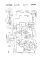
- FIG. 1 is a block diagram representing an embodiment of the present invention
- FIG. 2 is a data map representing a part of a read only memory (ROM) 11 shown in FIG. 1;
- FIG. 3 is a circuit diagram denoting a clock generator 19 shown in FIG. 1;
- FIG. 4 is a timing chart representing a circuit operation of the clock generator shown in FIG. 3;
- FIG. 5 is a timing chart representing a circuit operation of the circuit shown in FIG. 1;
- FIG. 6 is a pattern diagram showing a displayed character
- FIG. 7 is another diagram showing displayed characters.
- FIG. 8 is a circuit diagram representing a part of another embodiment of the present invention.
- a circuit diagram according to an embodiment of the present invention is shown.
- a television signal processing circuit 3 carries out a tuning function to a broadcasting signal received by an antenna 2 and detects the broadcasting signal.
- the circuit 3 further separates the detected signal into a sound information signal and a video information signal.
- the sound information signal is sound-detected, and a sound volume control is carried out to supply a sound signal S I to a loudspeaker 4.
- a vertical synchronizing pulse V S and a horizontal synchronizing pulse H S are picked out from the video information signal to produce vertical and horizontal deflection signals V D and H D .
- These signals V D and H D are supplied to a display 7.
- three primary color signal R, G and B having controlled brightness and contrast information are generated, and these signals R, G and B are supplied via a blanking control circuit 5 and an adder circuit 6 to the display 7.
- these signals R, G and B are supplied via a blanking control circuit 5 and an adder circuit 6 to the display 7.
- video pictures transmitted from a broadcasting station are reproduced on the display 7.
- the above-mentioned tuning operation in the television signal processing circuit 3 is carried out by the frequency synthesizer method using the PLL circuit under the control of a controller (microcomputer) 8 in response to an operated key or keys among channel selection keys provided in an input device 9.
- the input device 9 may be installed on a front panel of a television receiver set or may be represented as a remote control signal transmitter.
- the control of sound volume, brightness and contrast is performed digitally by the controller 8 in response to the operation of the associated key provided in the input device 9.
- the data for these controls are transmitted via data lines DL between the controller 8 and the circuit 3. The detailed description for those controls are omitted, because it is well-known by those skilled in the art and further does not directly relate to the present invention.
- the controller 8 is provided with a character generator for superimposing characters having an emphasizing contour on a video picture to display them on the display 7.
- the character generator is fabricated on one semiconductor substrate along with a processor 10, a read only memory (ROM) 11 and a random access memory (RAM) 12.
- the ROM 11 stores programs for instructing data processing of the processor 10.
- the RAM 12 is used as a data memory for program execution.
- the ROM 11 further stores character data to be displayed in accordance with the present invention.
- each character data are divided into contour data and character data.
- each contour data for each character has a size of ten picture elements on a horizontal line by sixteen picture elements on a vertical line.
- One picture element is made to correspond to one bit of the ROM 11. If the character data has a size of 10 ⁇ 16 bits like the contour data, the combined data of contour data and character data for each character has a size of 20 ⁇ 16 bits. Since each address of the ROM 11 is constructed with 16 bits, the data per one scan line for one character cannot be memorized in one address of the ROM 11. Two addresses are required. A great increase of memory capacity is thereby required. In this embodiment, therefore, the character data is compressed such that each character data consists of 5 ⁇ 10 bits. In other words, the data per one scan line of the character is compressed to 1/2, and the overall data for each character has a size of 15 ⁇ 16 bits. Thus, the data on one scan line can be stored in one address.
- the character data for the numbers "2" are stored in an area from “1120" (hexadecimal) address to "112F” address of the ROM 11 as shown in FIG. 2 and the contour data are stored from 0th bit (LBS) to 9th bit and the character data from 10th bit to 14th bit.
- LBS 0th bit
- the memory locations corresponding to the contour store bits "1", and the remaining locations store "0".
- the memory locations corresponding to horizonally-compressed character store "1", and the remaining locations store "0". Since the MSB is not used, its data may take “1” or "0” and is represented by mark "X" in the drawing.
- Memory locations for other characters "0", “1", “3” to “9” are also divided into the contour data part and the compressed character data part and their addresses are from "1100” to "110F”, “1110” to “111F”, “1130” to “113F”, . . . , and "1190” to "119F” of the ROM 11, respectively.
- the processor 10 when the controller 8 does not operate the character display, the processor 10 does not generate a character-on signal CON (this signal taking the low level).
- Multiplexers 13 and 14 select a ROM address counter 15 and a RAM address counter 16, respectively. Therefore, the processor 10 executes the instruction from the ROM 11 accessed by the ROM address counter 15. At this time, the RAM 12 is used as a data memory.
- the controller 8 When at least one of channel selection keys provided in the input device 9 is operated to receive a broadcasting wave signal at other than a non-receiving station, the controller 8 supplies data for switching a receiving-channel to the TV signal processing circuit 3. The controller 8 further generates data signals for displaying a number of the receiving-channel on the display 7. The circuit operation thereof will be described below for the case where the number of the receiving-channel is "2".
- the processor 10 writes the current starting address "1120" of the area of the ROM 11 wherein the character data "2" are stored into the address of the RAM 12 accessed by the RAM address counter 16.
- the count value of the counter 16 is incremented by one after a data-write operation, so that a next address of the RAM 12 is written.
- the fact that the data "FFFF" is written twice without a break means the end of the character display within one picture.
- a first stack register S 1 of a return address stack register 17 is thereafter written with data that represents the address of the RAM 12 in which the data "1120" is stored.
- the data written into the first stack register S 1 is "F000", for example, and is also stored in a RAM pointer 18. Since only one character display is carried out within one picture, a second stack register S 2 is not stored with any data.
- the processor 10 supplies via a data bus 117 to a clock generator 19 data for representing a display location of the character on the display 7.
- a high level character-on signal CON is thereafter generated by the processor 10.
- the multiplexer 14 selects the RAM pointer 18.
- the data stored in the RAM pointer 18 is supplied to the RAM 12.
- ROM pointer 20 which comprises an address latch part 20-1 and a counter part 20-2.
- the upper 12 bits data from the RAM 12 are latched in the address latch part 20-1.
- the value of the counter part 20-2 is 0. Since the multiplexer 13 selects the ROM pointer 20, the "1120" address of the ROM 11 is accessed and the data stored in the access address, i.e. "X000000001111000", are read out.
- the processor 10 carries out the above-mentioned operations during a high level period of the vertical synchronizing pulse Vs.
- the data from 0th bit to 9th bit i.e. the counter data
- the data from the 10th bit to 14th bit i.e. compressed character data
- the processor 10 generates a set pulse Sp in synchronism with the change from the high level to the low level of the horizontal synchronizing pulse Hs.
- This pulse Sp is supplied via an OR gate 23 to set terminals ⁇ of the shift registers 21 and 22.
- the contour data and the compressed character data are set into the shift registers 21 and 22, respectively.
- the clock generator 19 generates a shift clock CL to superimpose the character data on a video signal.
- the circuit construction of the clock generator 19 is shown in FIG. 3.
- Vertical direction character size data, horizontal direction character size data, vertical location data and horizontal location data produced by the processor 10 are stored into a counter 51, a counter 52, a latch circuit 53 and a latch circuit 56, respectively.
- the character size data are used to determine the vertical and horizontal direction sizes of one character.
- the counter 51 is set with, for example, "2”
- the counter 51 produces one pulse after receiving two horizontal synchronizing pulses Hs. Accordingly, the character size is expanded twice in a vertical direction.
- the data stored into the counters 51 and 52 are set to be "1", respectively.
- the outputs of the counters 51 and 52 are the same as the horizontal synchronizing pulse Hs and the clock pulse of an oscillator 50.
- One clock pulse from the oscillator 50 corresponds to one picture element of the display 7.
- the oscillator 50 is of a well-known synchronizing type that holds its output at the high level during a high level period of the pulse Hs.
- Clock pulses are generated after a predetermined time passes from the falling edge of the pulse Hs, as shown in FIG. 4.
- the outputs of the counters 51 and 52 are supplied respectively to clock terminals ⁇ of a line counter 54 and a dot counter 55.
- the counter receives the vertical synchronizing pulse Vs at its inverted preset control terminal P and introduces the data of the latch 53 in synchronism with the falling edge of the pulse Vs.
- the counter 55 receives the horizontal synchronizing pulse Hs at its preset control terminal P and introduces the data of the latch 56 in synchronism with the leading edge of the pulse Hs.
- the data stored in the latch circuits have starting location information of the character display. Assuming that the character display starting position is 6th horizontal scan line in a vertical direction and is 101th picture elements in a horizontal direction, the counters 54 and 55 are preset with "6" and "101", respectively. As shown in FIG.
- the counter 54 holds its output at the high level when it receives six horizontal synchronizing pulses Hs, and changes its output to the low level in synchronism with the falling edge of a next vertical synchronizing pulse Vs.
- the counter 55 holds its output at the high level when supplied with the clock pulses of 101 from the oscillator 50 and changes its output to the low level at the leading edge of a next horizontal synchronizing pulse Hs.
- the outputs of the counters 51 and 54 are supplied to an AND gate 57, and the outputs of the counter 52, 54 and 54 are supplied to an AND gate 58. Therefore, unless six horizontal synchronizing pulses Hs are supplied after the falling edge of the vertical synchronizing pulse Vs, any of output pulses LP, RE, CL, 1CE is not generated.
- the gate 51 take an open state.
- a shift clock pulses CL are generated as shown in FIG. 4.
- the shift clock CL is supplied to a one character counter 60. Since the number of bits in a horizontal direction of one character is ten, the counter 60 is preset with "11". Accordingly, the counter 60 generates a one character end pulse CE in synchronism with the eleventh shift clock CL.
- the gate takes an open state when six horizontal synchronizing pulses Hs are supplied, and produces pulses each time that the horizontal synchronizing pulses Hs are supplied until the vertical synchronizing pulse Vs is applied. These pulses are delayed by a delay circuit 61 to make line pulses LP.
- the pulses from the gate 57 are also supplied to a one row counter 59.
- the size in a vertical direction of one character is 16 bits. In other words, the character on one row corresponds to sixteen horizontal scan lines. Therefore, the counter 59 is present with "16", and generates a one row end pulse RE when the gate 57 produces sixteen output pulses, i.e. when twenty-one horizontal synchronizing pulses Hs are supplied.
- the leading edge of the pulse RE is approximately equal to that of the pulse LP.
- the clock generator 19 generates pulses CL, 1CE, LP and CE required for character display.
- the processor 10 since the processor 10 produces the set pulse Sp at the falling edge of the horizontal synchronizing pulse Hs, the data from 0th bit to 9th bit, "0001111000”, and the data from 10th bit to 14th bit, "0000", of the read out data from the ROM 11 are stored, respectively, into the shift registers 21 and 22 when the sixth horizontal synchronizing pulse Hs(6) is supplied after the falling edge of the vertical synchronizing pulse Vs.
- the line pulse LP generated from the clock generator 19 is supplied to the clock terminal ⁇ of the counter part 20-2 in the ROM pointer 20 to increment the value of the counter part 20-2 by one.
- the data stored in "1121" address of the ROM 11 is thereby read out.
- the shift register 22 receives shift clock pulses via a 1/2 divider 24. This is because one bit data stored in the register 22 corresponds to two picture elements. Since the data of the register 22 are "0000", its output continues to take the low level, as shown in FIG. 5. As S-R type flip-flop 32 is reset by the horizontal synchronizing pulse Hs, its inverted output Q produces a low level signal P1.
- each of AND gates 35 and 36 takes an open state, so that the signals from the registers 21 and 22 are outputted.
- the output of the AND gate 35 is supplied to the blanking control circuit 5.
- the circuit 5 changes its outputs to the low level during a high level output period of the AND gate 35 irrespective of the R, G and B signals from the TV circuit 3.
- the display 7 thereby takes a blanking condition during that period, so that the color "black” is displayed.
- the output of the AND gate 36 is supplied to the respective first input terminals of AND gates 38 and 40 whose second input terminals are supplied with a high level or a low level from a color data set circuit 37, respectively. Since the AND gate 36 produces the low level output, the outputs of the AND gates 38 to 40 take the low level irrespective of the level from the circuit 37. Accordingly, the adder circuit 6 produces only video picture information or blanking information.
- the clock generator 19 generates the one character end pulse 1CE in synchronism with the eleventh shift clock CL. Since the AND gate 29 is in an open state, the pulse 1CE is supplied to a clock terminal ⁇ of the RAM pointer 18 to increment the content thereof by one. The next address of the RAM 12 is thereby accessed. Since this address stored "FFFF", an all "F” detector 41 detects that data and produces a trigger pulse which is in turn supplied to a set terminal S of the flip-flop 32. A low signal P 1 is thus produced from the inverted output Q of the flip-flop 32, so that the AND gates 35 and 36 takes a closed state.
- the trigger signal from the detector 41 is also supplied to a first input terminal of an AND gate 27 whose second input terminal is supplied with the high level from an inverted output Q of a a flip-flop 26 taking a reset state. Since the one row end pulse RE is not generated, a stack pointer 25 points to the first stack register S1. Therefore, the data stored in the first register S1 is written as a return address into the RAM pointer 19 in synchronism with the trigger signal. The RAM pointer 18 thus takes its content representing the address of the RAM 12 in which the data "1120" is stored. The trigger signal from the detector 41 disappears before the flip-flop 32 produces the high level at its output Q, so that the AND gate 28 continues to take the closed state. Thus, the character data processing on one horizontal scan line is completed.
- the set pulse Sp is generated to set output data from 0th bit to 9th bit (0010000100) and the output data from 10th bit to 14th bit (01110) which are read out from "1121" address of the ROM 11 into the shift registers 21 and 22, respectively.
- the flip-flop 32 is changed to the reset state, and the flip-flop 26 holds the reset state.
- the above-mentioned operations occur, so that the shift registers 21 and 22 produce the output signal shown in FIG. 5, respectively. Since the shift register receives a 1/2 frequency clock from the divider 24 as a shift clock, the high level period of the output of the register 22 corresponds to six cycle periods of the shift clock CL.
- the compressed data "01110” is expanded to "0011111100".
- the output of the shift register 22 is inverted by an inverter 33, and the inverter signal "1100000011” is supplied to a NOR gate together with the output of the shift register 21 "0010000100". Accordingly, the output of the AND gate 36 takes the high level during a period intervening between two high levels in the output of the AND gate 35. In the above-mentioned examples, its output is "0001111000".
- the error data contained in expanded character data is corrected. That is, the error data "1" of the location where character overlaps with the contour is converted into "0".
- the circuit 37 supplies the high level to each of the AND gates 38 to 40.
- the data of "112F" address of the ROM 11 are set into the shift register 21 and 22, and the data shift operation is carried out.
- the clock generator 19 generates the one row end pulse RE.
- This pulse RE is supplied to a reset terminal R of the ROM pointer 20 to reset it.
- the pulse RE is also supplied to a set terminal S of the flip-flop 26, so that an inverted output Q thereof takes the low level.
- the gate 27 thereby takes the closed state, and the gate 42 takes the open state.
- the content of the RAM pointer 18 is incremented by one to access the next address of the RAM 11.
- the detector 41 Since that address stores the data of "FFFF", the detector 41 produces the trigger signal to set the flip-flop 32. Since the gate 27 is in the closed state, the trigger signal is not supplied to the stack pointer 25. When eleven shift clocks are further generated as shown in FIG. 5, the pulse CE is supplied via the gate 42 to the RAM pointer 18. A further next address of the RAM 12 is thereby accessed. Since that address stores the data of "FFFF”, the detector 41 produces again the trigger pulse. This pulse is supplied via the gate 28 to a reset terminal R of the RAM pointer 18 and further to the processor 10 as a character display end pulse CEND. The RAM pointer 18 is thereby reset. As a result, the character display on one video picture is completed. When the vertical synchronizing pulse Vs is thereafter supplied, the data write operation is carried out during the high level period of the pulse Vs and the above-mentioned operation is performed.
- the character having an emphasizing contour is displayed in the display 7, as shown in FIG. 6.
- the portions denoted in hatching represent the blanking state of the display 7 as the contour portion, and are thus displayed in black.
- the inside portion of the contour portion, that is, the character portion (dotted area) is displayed in green color, and the video picture is displayed on the outside of the contour.
- the second stack register S2 is stored with a return address of a second row character.
- more than two stack registers are provided, and return addresses of the respective rows are stored in the associated stack register. The operation of character display of two rows will be described below.
- the data of "1130" appears on the output of the ROM pointer 20. Since the stack pointer 25 points the second stack register S 2 in response to the pulse RE which is generated at the end of character display of the first row, the RAM pointer 18 is stored with the data of "F002" as a return address when the display one horizontal scan line in the second row is completed. As a result, the characters shown in FIG. 7 are displayed on the display 7.
- FIG. 8 shows a part of another embodiment of the present invention, in which the same constituents as those shown in FIG. 1 are denoted the same reference numerals to omit the further explanation thereof.
- the 15th bit (MSB) of the ROM 11 is also utilized to control the character display. More particularly, the 15th bit (MSB) of the ROM 11 is stored into a latch circuit 99 in response to the set pulse to the shift registers 21 and 22. The output of the latch 99 is supplied to a first input terminal of an AND gate 100 whose second input terminal is supplied with the output of the shift register 22. When the MSB of the ROM 11 is written with "1", the gate takes an open state. In this case, the circuit operation is the same as that of the circuit shown in FIG. 1.
- the gate 100 may be provided on the side of the output of the inverter 33, NOR gate 34, and AND gate 36.
- Characters other than a numeral can be displayed, and one character can be displayed over a plurality of rows.
- contour data can be compressed in place of the compression of the character data.
Abstract
Description
Claims (7)
Applications Claiming Priority (2)
| Application Number | Priority Date | Filing Date | Title |
|---|---|---|---|
| JP61129582A JPS6323189A (en) | 1986-06-03 | 1986-06-03 | Symbol generation circuit |
| JP61-129582 | 1986-06-03 |
Publications (1)
| Publication Number | Publication Date |
|---|---|
| US4794451A true US4794451A (en) | 1988-12-27 |
Family
ID=15013019
Family Applications (1)
| Application Number | Title | Priority Date | Filing Date |
|---|---|---|---|
| US07/057,146 Expired - Lifetime US4794451A (en) | 1986-06-03 | 1987-06-03 | Signal generator generating character data having contour |
Country Status (4)
| Country | Link |
|---|---|
| US (1) | US4794451A (en) |
| EP (1) | EP0250906B1 (en) |
| JP (1) | JPS6323189A (en) |
| DE (1) | DE3750442T2 (en) |
Cited By (8)
| Publication number | Priority date | Publication date | Assignee | Title |
|---|---|---|---|---|
| US4962465A (en) * | 1987-12-28 | 1990-10-09 | Sharp Kabushiki Kaisha | Character processor provided with dot pattern correcting function |
| US5200739A (en) * | 1989-04-20 | 1993-04-06 | U.S. Philips Corporation | Character generator for displaying characters with a shadow on a display screen |
| US5201032A (en) * | 1988-06-02 | 1993-04-06 | Ricoh Company, Ltd. | Method and apparatus for generating multi-level character |
| US5225819A (en) * | 1989-05-12 | 1993-07-06 | Mitsubishi Denki Kabushiki Kaisha | Screen display device |
| US5479184A (en) * | 1988-09-06 | 1995-12-26 | Kabushiki Kaisha Toshiba | Videotex terminal system using CRT display and binary-type LCD display |
| US6126342A (en) * | 1988-08-31 | 2000-10-03 | Canon Kabushiki Kaisha | Output device capable of high quality output of characters over a large range of sizes |
| US6128409A (en) * | 1991-11-12 | 2000-10-03 | Texas Instruments Incorporated | Systems and methods for handprint recognition acceleration |
| US6249273B1 (en) * | 1992-11-14 | 2001-06-19 | U.S. Philips Corp. | Method of and device for displaying characters with a border |
Citations (4)
| Publication number | Priority date | Publication date | Assignee | Title |
|---|---|---|---|---|
| US3984828A (en) * | 1975-05-23 | 1976-10-05 | Rca Corporation | Character generator for television channel number display with edging provisions |
| US4020462A (en) * | 1975-12-08 | 1977-04-26 | International Business Machines Corporation | Method and apparatus for form removal from contour compressed image data |
| US4437092A (en) * | 1981-08-12 | 1984-03-13 | International Business Machines Corporation | Color video display system having programmable border color |
| US4466123A (en) * | 1981-07-10 | 1984-08-14 | Fuji Xerox Co., Ltd. | Apparatus and method for correcting contour line pattern images |
Family Cites Families (3)
| Publication number | Priority date | Publication date | Assignee | Title |
|---|---|---|---|---|
| DE2819286C3 (en) * | 1978-05-02 | 1981-01-22 | Siemens Ag, 1000 Berlin Und 8000 Muenchen | Circuit arrangement for improving the display quality when displaying characters on screens of display devices operating on the grid principle |
| US4408198A (en) * | 1981-09-14 | 1983-10-04 | Shintron Company, Inc. | Video character generator |
| JPS6075968A (en) * | 1983-10-03 | 1985-04-30 | Photo Composing Mach Mfg Co Ltd | Revolution processing method of character picture data |
-
1986
- 1986-06-03 JP JP61129582A patent/JPS6323189A/en active Pending
-
1987
- 1987-06-03 US US07/057,146 patent/US4794451A/en not_active Expired - Lifetime
- 1987-06-03 DE DE3750442T patent/DE3750442T2/en not_active Expired - Fee Related
- 1987-06-03 EP EP87108027A patent/EP0250906B1/en not_active Expired - Lifetime
Patent Citations (4)
| Publication number | Priority date | Publication date | Assignee | Title |
|---|---|---|---|---|
| US3984828A (en) * | 1975-05-23 | 1976-10-05 | Rca Corporation | Character generator for television channel number display with edging provisions |
| US4020462A (en) * | 1975-12-08 | 1977-04-26 | International Business Machines Corporation | Method and apparatus for form removal from contour compressed image data |
| US4466123A (en) * | 1981-07-10 | 1984-08-14 | Fuji Xerox Co., Ltd. | Apparatus and method for correcting contour line pattern images |
| US4437092A (en) * | 1981-08-12 | 1984-03-13 | International Business Machines Corporation | Color video display system having programmable border color |
Cited By (8)
| Publication number | Priority date | Publication date | Assignee | Title |
|---|---|---|---|---|
| US4962465A (en) * | 1987-12-28 | 1990-10-09 | Sharp Kabushiki Kaisha | Character processor provided with dot pattern correcting function |
| US5201032A (en) * | 1988-06-02 | 1993-04-06 | Ricoh Company, Ltd. | Method and apparatus for generating multi-level character |
| US6126342A (en) * | 1988-08-31 | 2000-10-03 | Canon Kabushiki Kaisha | Output device capable of high quality output of characters over a large range of sizes |
| US5479184A (en) * | 1988-09-06 | 1995-12-26 | Kabushiki Kaisha Toshiba | Videotex terminal system using CRT display and binary-type LCD display |
| US5200739A (en) * | 1989-04-20 | 1993-04-06 | U.S. Philips Corporation | Character generator for displaying characters with a shadow on a display screen |
| US5225819A (en) * | 1989-05-12 | 1993-07-06 | Mitsubishi Denki Kabushiki Kaisha | Screen display device |
| US6128409A (en) * | 1991-11-12 | 2000-10-03 | Texas Instruments Incorporated | Systems and methods for handprint recognition acceleration |
| US6249273B1 (en) * | 1992-11-14 | 2001-06-19 | U.S. Philips Corp. | Method of and device for displaying characters with a border |
Also Published As
| Publication number | Publication date |
|---|---|
| JPS6323189A (en) | 1988-01-30 |
| DE3750442T2 (en) | 1995-03-30 |
| DE3750442D1 (en) | 1994-10-06 |
| EP0250906B1 (en) | 1994-08-31 |
| EP0250906A3 (en) | 1990-09-19 |
| EP0250906A2 (en) | 1988-01-07 |
Similar Documents
| Publication | Publication Date | Title |
|---|---|---|
| CA1229908A (en) | Crt display control device | |
| EP0301488B1 (en) | Television receiver having a memorandum function | |
| JPS646477B2 (en) | ||
| US5479184A (en) | Videotex terminal system using CRT display and binary-type LCD display | |
| US5206714A (en) | Circuit for controlling the time interval between rotational movements of a plurality of subordinate pictures in a picture-in-picture-type television or VTR system and method therefor | |
| US4794451A (en) | Signal generator generating character data having contour | |
| US4811099A (en) | Video signal memories | |
| US5202669A (en) | Display control device for superimposing data with a broadcast signal on a television screen | |
| KR0174536B1 (en) | Receiver for television signals | |
| KR100275188B1 (en) | Character display apparatus | |
| US4471377A (en) | Color information display apparatus | |
| US5339160A (en) | Character display device for synchronizing operation of video ram to operation of CPU | |
| US5200739A (en) | Character generator for displaying characters with a shadow on a display screen | |
| US4959793A (en) | Microcomputer having function of generating data signals used for displaying characters | |
| US4766496A (en) | Video signal memories | |
| KR0182809B1 (en) | Character generator | |
| JP2562727B2 (en) | Display microcomputer | |
| JP2822668B2 (en) | Display control device | |
| JP2591064B2 (en) | Teletext broadcast receiver | |
| JPH06268908A (en) | Frame signal generating circuit for multiscreen | |
| JP2597983B2 (en) | Multi-screen TV receiver | |
| JP2781924B2 (en) | Superimpose device | |
| JPS62192794A (en) | Image synthetic display unit | |
| KR890007597A (en) | Video signal generator | |
| JPH04366995A (en) | Video display device |
Legal Events
| Date | Code | Title | Description |
|---|---|---|---|
| AS | Assignment |
Owner name: NEC CORPORATION, 33-1, SHIBA 5-CHOME, MINATO-KU, T Free format text: ASSIGNMENT OF ASSIGNORS INTEREST.;ASSIGNORS:SUZUKI, HIROYUKI;KAWATA, KAZUHIDE;REEL/FRAME:004943/0498 Effective date: 19870603 Owner name: NEC CORPORATION,JAPAN Free format text: ASSIGNMENT OF ASSIGNORS INTEREST;ASSIGNORS:SUZUKI, HIROYUKI;KAWATA, KAZUHIDE;REEL/FRAME:004943/0498 Effective date: 19870603 |
|
| STCF | Information on status: patent grant |
Free format text: PATENTED CASE |
|
| FEPP | Fee payment procedure |
Free format text: PAYOR NUMBER ASSIGNED (ORIGINAL EVENT CODE: ASPN); ENTITY STATUS OF PATENT OWNER: LARGE ENTITY |
|
| FPAY | Fee payment |
Year of fee payment: 4 |
|
| FPAY | Fee payment |
Year of fee payment: 8 |
|
| FEPP | Fee payment procedure |
Free format text: PAYER NUMBER DE-ASSIGNED (ORIGINAL EVENT CODE: RMPN); ENTITY STATUS OF PATENT OWNER: LARGE ENTITY |
|
| FEPP | Fee payment procedure |
Free format text: PAYOR NUMBER ASSIGNED (ORIGINAL EVENT CODE: ASPN); ENTITY STATUS OF PATENT OWNER: LARGE ENTITY |
|
| FPAY | Fee payment |
Year of fee payment: 12 |
|
| AS | Assignment |
Owner name: NEC ELECTRONICS CORPORATION, JAPAN Free format text: ASSIGNMENT OF ASSIGNORS INTEREST;ASSIGNOR:NEC CORPORATION;REEL/FRAME:013758/0440 Effective date: 20021101 |