US4841167A - Clock recovering device - Google Patents
Clock recovering device Download PDFInfo
- Publication number
- US4841167A US4841167A US07/089,794 US8979487A US4841167A US 4841167 A US4841167 A US 4841167A US 8979487 A US8979487 A US 8979487A US 4841167 A US4841167 A US 4841167A
- Authority
- US
- United States
- Prior art keywords
- clock
- counter
- output
- recovering device
- received data
- Prior art date
- Legal status (The legal status is an assumption and is not a legal conclusion. Google has not performed a legal analysis and makes no representation as to the accuracy of the status listed.)
- Expired - Fee Related
Links
Images


Classifications
-
- G—PHYSICS
- G06—COMPUTING; CALCULATING OR COUNTING
- G06F—ELECTRIC DIGITAL DATA PROCESSING
- G06F1/00—Details not covered by groups G06F3/00 - G06F13/00 and G06F21/00
- G06F1/04—Generating or distributing clock signals or signals derived directly therefrom
-
- H—ELECTRICITY
- H04—ELECTRIC COMMUNICATION TECHNIQUE
- H04L—TRANSMISSION OF DIGITAL INFORMATION, e.g. TELEGRAPHIC COMMUNICATION
- H04L7/00—Arrangements for synchronising receiver with transmitter
- H04L7/02—Speed or phase control by the received code signals, the signals containing no special synchronisation information
- H04L7/033—Speed or phase control by the received code signals, the signals containing no special synchronisation information using the transitions of the received signal to control the phase of the synchronising-signal-generating means, e.g. using a phase-locked loop
- H04L7/0331—Speed or phase control by the received code signals, the signals containing no special synchronisation information using the transitions of the received signal to control the phase of the synchronising-signal-generating means, e.g. using a phase-locked loop with a digital phase-locked loop [PLL] processing binary samples, e.g. add/subtract logic for correction of receiver clock
Definitions
- the present invention relates to a clock recovering device and, more particularly, to a device for accurately recovering a clock from received data which has a different duty ratio of logical ONEs and logical ZEROs.
- a prior art clock recovering device corrects the phase of a recovered clock timed to transitions of received data.
- a problem with such a device is that when the duty ratio of ONEs and ZEROs of received data is different, even if the phase of a recovered clock is greatly deviated, the phase is decided as being advanced and retarded alternately every time a transition is detected. This indefinitely prevents a clock from being correctly recovered.
- an object of the present invention to provide a clock recovering device capable of accurately recovering a clock from received data despite a difference of duty ratio.
- a clock recovering device of the present invention comprises an edge detector for producing a pulse when received data changes, a first counter for counting a high-speed clock which is an integral multiple times higher than a transmission rate of the received data, and reset by the pulse output by the edge detector, a logic unit for processing an output of the first counter, a second counter for receiving an output of the logic unit and reset by the pulse for counting the high-speed clock, a phase comparator for deciding a phase of recovered clock timed to a carry which is output by the second counter, and a variable frequency divider controlled in frequency division number by an output of the phase comparator for producing the recovered clock from the high-speed clock.
- a device for recovering a clock from received data which has a different duty ratio determines the optimum timing of a recovered clock based on the pulse width of the received data.
- a clock is accurately recovered so long as the duty ratio of received data is not greater than ⁇ 50%.
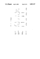
- FIGS. 1 and 2 are timing charts demonstrating the operation of a prior art clock recovering device
- FIG. 3 is a block diagram showing a clock recovering device embodying the present invention.
- FIG. 4 is a timing chart representative of the operation of the clock recovering device in accordance with the present invention.
- FIG. 5 is a block diagram showing another embodiment of the present invention.
- FIG. 6 is a chart showing data stored in a ROM (Read Only Memory) which is included in the device of FIG. 5.
- ROM Read Only Memory
- FIG. 1 it is a common practice to correct the phase of recovered clock by detecting a transition of received data and, if the recovered clock is low level at the instant of detection of a transition, retarding the phase deciding that the phase is advanced and, if it is high level, advancing the phase deciding that the phase is retarded.
- a prior art implementation indefinitely fails to correctly recover a clock if the duty ratio is not greater than ⁇ 50%, because, as shown in FIG. 2, the phase is decided as being advanced and retarded alternately timed to the transitions of received data even if the phase of the recovered clock is greatly deviated.
- the clock recovering device comprises an edge detector 12 to which received data 13 is applied, a first n-bit binary counter 14 which is supplied with an output 12a of the edge detector 12, a second n-bit binary counter 16 which is also supplied with the output 12a of the edge detector 12, an inverter 18 connected to the first n-bit binary counter 14, a phase comparator 20 to which an output 16a of the second n-bit binary counter 16 is coupled, and a variable frequency divider 22 which receives an output 20a of the phase comparator 20 and, in turn, feeds its output 22a to the phase comparator 20.
- the width of a logical high or a logical low pulse of the received data 13 is T p
- the period of the received data 13 is T o
- the deviation of duty is greater than -50% and smaller than +50%.
- the data length is 1, the timing of recovered clock is 0.5T p before because T p is equal to or greater than 0.5T o and smaller than 1.5T o ; if the data length is 2, the timing of recovered clock is 0.5 (T p -T o ) before because T p is equal to or greater than 1.5T o and smaller than 2.5T o ; if the data length is 3, the timing of recovered clock is 0.5 (T p -2T o ) before because T p is equal to or greater than 2.5T o and smaller than 3.5T o ; and if the data length is m, the timing of recovered clock is 0.5[T p -(m-1)T o ] before because T p is equal to or greater than (m-
- the edge detector 12 Upon transition of the received data 13 from high to or low or vice versa, the edge detector 12 produces a pulse 12a.
- the first n-bit binary counter 14 counts a high-speed clock 24 which is 2 n times higher than the transmission rate of received data.
- the counter 14 is reset by each pulse 12a to reach the same count at every period T, so that the count ⁇ immediately before resetting is produced by: ##EQU1##
- the "n-1" to “1" bit outputs of the first n-bit binary counter 14 are connected to, respectively, the “n-2" to “0” bit inputs of the second n-bit binary counter 16. Further, the "n-1" bit output of the first counter 14 is connected to the "n-1” bit input of the second counter 16 by way of the inverter 18. Assuming that the value read in response to the pulse 12a is K, there holds an equation: ##EQU3## Hence, what is stored in the second n-bit binary counter 16 is a time interval between the optimum timing of recovered clock and a transition of received data.
- the second n-bit binary counter 16 continuously counts the high-speed clock 24, its carry 16a coincides in timing with the optimum timing of recovered clock.
- the carry 16a and the recovered clock 22a are fed to the phase comparator 20 which then decides the phase of the recovered clock 22a and produces a phase correct signal 20a.
- the variable frequency divider 22 changes the frequency division number to thereby correct the phase of the recovered clock 22a.
- FIG. 5 another embodiment of the present invention is shown.
- This embodiment is essentially the same in construction as the embodiment of FIG. 3 except for the provision of a first and a second modulo N counter 26 and 28 and a ROM 30 which serves as a decoder.
- the clock recovering device of FIG. 5 recovers a clock in the same manner as the device of FIG. 3, when N is 8.
- the edge detector 12 produces a pulse 12a.
- the high-speed clock 24 which is N times higher than the received data transmission rate
- the first N modulo counter 26 is reset by each pulse 12a to reach the same count at each period T.
- the count M immediately before resetting is produced by: ##EQU4##
- the "0", “1”, . . . , “n-1” bit outputs of the first modulo N counter 26 are fed to, respectively, the "A 0 ", “A 1 ", . . . , “A n-1 " bits of the ROM 30.
- the second modulo N counter 28, therefore, is loaded with a time interval between the optimum timing of recovered clock and a transition of received data.
- the second modulo N counter 28 Since the second modulo N counter 28, too, has a period of T o , its carry 28a coincides in timing with the optimum timing of recovered clock. Subsequently, as in the first embodiment, the carry 28a and the recovered clock 22a are applied to the phase comparator 20. In response, the phase comparator 20 decides the phase of the recovered clock 22a and, then, produces a phase correct signal 20a. The variable frequency divider 22 changes the frequency division number by using the phase correct signal 20a, thereby correcting the phase of the recovered clock 22a.
- the present invention provides a clock recovering device which accurately recovers a clock if the duty ratio of received data is not greater than ⁇ 50%, because it determines the optimum timing of recovered clock based on the pulse width of received data.
Abstract
A device for recovering a clock from received data which has a different duty ratio is disclosed. The optimum timing of a recovered clock is determined based on the pulse width of received data. A clock is accurately recovered so long as the duty ratio of received data is not greater than ±50%.
Description
The present invention relates to a clock recovering device and, more particularly, to a device for accurately recovering a clock from received data which has a different duty ratio of logical ONEs and logical ZEROs.
For the recovery of a clock from received data, it has been customary to detect a transition of the incoming data and, if the recovered clock is low level (or high level) at the instant of detection of a transition, retard (or advance) the phase of the recovered clock deciding that the phase is advanced (or retarded). In this manner, a prior art clock recovering device corrects the phase of a recovered clock timed to transitions of received data. However, a problem with such a device is that when the duty ratio of ONEs and ZEROs of received data is different, even if the phase of a recovered clock is greatly deviated, the phase is decided as being advanced and retarded alternately every time a transition is detected. This indefinitely prevents a clock from being correctly recovered.
It is, therefore, an object of the present invention to provide a clock recovering device capable of accurately recovering a clock from received data despite a difference of duty ratio.
It is another object of the present invention to provide a generally improved clock recovering device.
A clock recovering device of the present invention comprises an edge detector for producing a pulse when received data changes, a first counter for counting a high-speed clock which is an integral multiple times higher than a transmission rate of the received data, and reset by the pulse output by the edge detector, a logic unit for processing an output of the first counter, a second counter for receiving an output of the logic unit and reset by the pulse for counting the high-speed clock, a phase comparator for deciding a phase of recovered clock timed to a carry which is output by the second counter, and a variable frequency divider controlled in frequency division number by an output of the phase comparator for producing the recovered clock from the high-speed clock.
In accordance with the present invention, a device for recovering a clock from received data which has a different duty ratio determines the optimum timing of a recovered clock based on the pulse width of the received data. A clock is accurately recovered so long as the duty ratio of received data is not greater than ±50%.
FIGS. 1 and 2 are timing charts demonstrating the operation of a prior art clock recovering device;
FIG. 3 is a block diagram showing a clock recovering device embodying the present invention;
FIG. 4 is a timing chart representative of the operation of the clock recovering device in accordance with the present invention;
FIG. 5 is a block diagram showing another embodiment of the present invention; and
FIG. 6 is a chart showing data stored in a ROM (Read Only Memory) which is included in the device of FIG. 5.
To better understand the present invention, the operation of a prior art clock recovering device will be outlined with reference to FIGS. 1 and 2. As shown in FIG. 1, it is a common practice to correct the phase of recovered clock by detecting a transition of received data and, if the recovered clock is low level at the instant of detection of a transition, retarding the phase deciding that the phase is advanced and, if it is high level, advancing the phase deciding that the phase is retarded. As previously stated, such a prior art implementation indefinitely fails to correctly recover a clock if the duty ratio is not greater than ±50%, because, as shown in FIG. 2, the phase is decided as being advanced and retarded alternately timed to the transitions of received data even if the phase of the recovered clock is greatly deviated.
Referring to FIG. 3, a clock recovering device embodying the present invention and which is free from the drawback discussed above is shown. The clock recovering device, generally 10, comprises an edge detector 12 to which received data 13 is applied, a first n-bit binary counter 14 which is supplied with an output 12a of the edge detector 12, a second n-bit binary counter 16 which is also supplied with the output 12a of the edge detector 12, an inverter 18 connected to the first n-bit binary counter 14, a phase comparator 20 to which an output 16a of the second n-bit binary counter 16 is coupled, and a variable frequency divider 22 which receives an output 20a of the phase comparator 20 and, in turn, feeds its output 22a to the phase comparator 20.
The operation of the clock recovering device 10 will be described with reference to FIG. 4. In the figure, "n" is assumed to be 3.
Assume that the width of a logical high or a logical low pulse of the received data 13 is Tp, the period of the received data 13 is To, and the deviation of duty is greater than -50% and smaller than +50%. Then, if the data length is 1, the timing of recovered clock is 0.5Tp before because Tp is equal to or greater than 0.5To and smaller than 1.5To ; if the data length is 2, the timing of recovered clock is 0.5 (Tp -To) before because Tp is equal to or greater than 1.5To and smaller than 2.5To ; if the data length is 3, the timing of recovered clock is 0.5 (Tp -2To) before because Tp is equal to or greater than 2.5To and smaller than 3.5To ; and if the data length is m, the timing of recovered clock is 0.5[Tp -(m-1)To ] before because Tp is equal to or greater than (m-0.5)To and smaller than (m+0.5)To.
Upon transition of the received data 13 from high to or low or vice versa, the edge detector 12 produces a pulse 12a. The first n-bit binary counter 14 counts a high-speed clock 24 which is 2n times higher than the transmission rate of received data. The counter 14 is reset by each pulse 12a to reach the same count at every period T, so that the count ι immediately before resetting is produced by: ##EQU1##
Since a relation 2n-1 ≦1<2n -1 holds under a condition of (m-0.5)To <Tp <mTo and a relation 0≦1<2n-1 holds under a condition of mTo ≦Tp <(m+0.5)To, the timing of recovered clock is expressed as: ##EQU2##
As shown in FIG. 3, the "n-1" to "1" bit outputs of the first n-bit binary counter 14 are connected to, respectively, the "n-2" to "0" bit inputs of the second n-bit binary counter 16. Further, the "n-1" bit output of the first counter 14 is connected to the "n-1" bit input of the second counter 16 by way of the inverter 18. Assuming that the value read in response to the pulse 12a is K, there holds an equation: ##EQU3## Hence, what is stored in the second n-bit binary counter 16 is a time interval between the optimum timing of recovered clock and a transition of received data.
Since the second n-bit binary counter 16 continuously counts the high-speed clock 24, its carry 16a coincides in timing with the optimum timing of recovered clock. The carry 16a and the recovered clock 22a are fed to the phase comparator 20 which then decides the phase of the recovered clock 22a and produces a phase correct signal 20a. In response, the variable frequency divider 22 changes the frequency division number to thereby correct the phase of the recovered clock 22a.
Referring to FIG. 5, another embodiment of the present invention is shown. This embodiment is essentially the same in construction as the embodiment of FIG. 3 except for the provision of a first and a second modulo N counter 26 and 28 and a ROM 30 which serves as a decoder. By the operation which will be described, the clock recovering device of FIG. 5 recovers a clock in the same manner as the device of FIG. 3, when N is 8. The ROM 30 computes L=0.5N+0.5M (where M<0.5N) and L=0.5M (where M>0.5N) based on a count m of the first N-bit counter 26.
Turning back to FIG. 4, as the received data 13 changes from high to low or vice versa, the edge detector 12 produces a pulse 12a. Counting the high-speed clock 24 which is N times higher than the received data transmission rate, the first N modulo counter 26 is reset by each pulse 12a to reach the same count at each period T. Hence, the count M immediately before resetting is produced by: ##EQU4##
Since M is the count of the N-bit counter, relations M≧0.5N and M<0.5N hold under conditions of (m-0.5)To ≦Tp <mTo and mTo ≦Tp ≦(m+0.5)To, respectively. Further, there holds an equation: ##EQU5##
Therefore, the timing of recovered clock is produced by: ##EQU6##
The "0", "1", . . . , "n-1" bit outputs of the first modulo N counter 26 are fed to, respectively, the "A0 ", "A1 ", . . . , "An-1 " bits of the ROM 30. The ROM 30 computes L=0.5M (M≧0.5N) and L=0.5N+0.5M (M<0.5N) (data stored in the ROM 30 when N is 8 are shown in FIG. 6), the results appearing on the "O0 ", "O1 ", . . . , "On-1 " bits. The second modulo N counter 28, therefore, is loaded with a time interval between the optimum timing of recovered clock and a transition of received data.
Since the second modulo N counter 28, too, has a period of To, its carry 28a coincides in timing with the optimum timing of recovered clock. Subsequently, as in the first embodiment, the carry 28a and the recovered clock 22a are applied to the phase comparator 20. In response, the phase comparator 20 decides the phase of the recovered clock 22a and, then, produces a phase correct signal 20a. The variable frequency divider 22 changes the frequency division number by using the phase correct signal 20a, thereby correcting the phase of the recovered clock 22a.
In summary, it will be seen that the present invention provides a clock recovering device which accurately recovers a clock if the duty ratio of received data is not greater than ±50%, because it determines the optimum timing of recovered clock based on the pulse width of received data.
Various modifications will become possible for those skilled in the art after receiving the teachings of the present disclosure without departing from the scope thereof.
Claims (7)
1. A clock recovering device comprising:
an edge detector means for producing a pulse when received data changes;
a first counter means for counting a high-speed clock which is an integral multiple times higher than a transmission rate of the received data, and reset by the pulse output of said edge detector means;
a logic means for processing an output of said first counter means;
a second counter means for receiving an output of said logic means and reset by the pulse output for counting the high-speed clock;
a phase comparator means for deciding a phase of recovered clock by comparing the recovered clock with a carry which is output by said second counter means; and
a variable frequency divider means controlled in frequency division number by an output of said phase comparator means for producing the recovered clock from the high-speed clock.
2. A clock recovering device as claimed in claim 1, wherein said first counter means comprises a first n-bit binary counter for counting a high-speed clock which is 2n times higher than the transmission rate of the received data, and reset by the pulse.
3. A clock recovering device as claimed in claim 2, wherein said logic means comprises an inverter for inverting an "n-1" bit output of said first n-bit binary counter.
4. A clock recovering device as claimed in claim 3, wherein said second counter means comprises a second n-bit binary counter having an "n-1" bit input to which an output of said inverter is connected and an "n-2" to a "0" bit input to which an "n-1" to a "1" bit output of said first n-bit binary counter are respectively connected, so as to read data in response to the pulse, and counting the high-speed clock.
5. A clock recovering device as claimed in claim 1, wherein said first counter means comprises a first modulo N counter for counting a high-speed clock which is N times higher than the transmission rate of the received data, and reset by the pulse.
6. A clock recovering device as claimed in claim 5, wherein said logic means comprises a decoder for computing L=0.5N+0.5M (M<0.5N) and L=0.5M (M>0.5N) by using a count M of said first modulo N counter.
7. A clock recovering device as claimed in claim 6, wherein said second counter means comprises a second modulo N counter for counting the high-speed clock and set to an initial value L by the pulse.
Applications Claiming Priority (1)
| Application Number | Priority Date | Filing Date | Title |
|---|---|---|---|
| JP19903986 | 1986-08-27 |
Publications (1)
| Publication Number | Publication Date |
|---|---|
| US4841167A true US4841167A (en) | 1989-06-20 |
Family
ID=16401102
Family Applications (1)
| Application Number | Title | Priority Date | Filing Date |
|---|---|---|---|
| US07/089,794 Expired - Fee Related US4841167A (en) | 1986-08-27 | 1987-08-27 | Clock recovering device |
Country Status (7)
| Country | Link |
|---|---|
| US (1) | US4841167A (en) |
| EP (1) | EP0261428B1 (en) |
| JP (1) | JPH0770991B2 (en) |
| KR (1) | KR910001556B1 (en) |
| AU (1) | AU600871B2 (en) |
| CA (1) | CA1274883A (en) |
| DE (1) | DE3788030D1 (en) |
Cited By (16)
| Publication number | Priority date | Publication date | Assignee | Title |
|---|---|---|---|---|
| US5003562A (en) * | 1989-10-27 | 1991-03-26 | Ncr Corporation | Digital phase lock loop decoder |
| US5012198A (en) * | 1988-09-29 | 1991-04-30 | Mitsubishi Rayon Company, Ltd. | Digital PLL circuit having reduced lead-in time |
| US5134637A (en) * | 1991-03-22 | 1992-07-28 | Motorola, Inc. | Clock recovery enhancement circuit |
| US5319681A (en) * | 1991-07-30 | 1994-06-07 | Sgs-Thomson Microelectronics S.A. | Method and a device for synchronizing a signal |
| EP0715428A2 (en) * | 1994-11-30 | 1996-06-05 | Alcatel SEL Aktiengesellschaft | Synchronisation monitoring in a network element |
| US5694066A (en) * | 1995-11-28 | 1997-12-02 | Industrial Research Institute | Low-jitter, non-slip clock generator |
| US5784332A (en) * | 1996-12-12 | 1998-07-21 | Micron Technology Corporation | Clock frequency detector for a synchronous memory device |
| US5793821A (en) * | 1995-06-07 | 1998-08-11 | 3Com Corporation | Timing Recovery using group delay compensation |
| US6212111B1 (en) | 1997-04-25 | 2001-04-03 | Micron Technology, Inc. | Synchronous dynamic random access memory device |
| US6239635B1 (en) * | 1998-07-06 | 2001-05-29 | Fujitsu Limited | Self-timing control circuit |
| US20030099319A1 (en) * | 2001-11-20 | 2003-05-29 | Bailey Daniel William | Expanded comparator for control of digital delay lines in a delay locked loop or phase locked loop |
| US20040061540A1 (en) * | 2001-02-27 | 2004-04-01 | Ejima Ken?Apos;Ichi | Clock reproduction circuit |
| US20050185720A1 (en) * | 2004-02-24 | 2005-08-25 | Kwok Chung Y. | Pseudo-synchronous one wire bidirectional bus interface |
| US20080265961A1 (en) * | 2007-04-27 | 2008-10-30 | Semiconductor Energy Laboratory Co., Ltd. | Clock signal generation circuit and semiconductor device |
| US20090268845A1 (en) * | 2004-11-18 | 2009-10-29 | Broadcom Corporation | Radio transmitter incorporating digital modulator and circuitry to accommodate baseband processor with analog interface |
| US9712173B2 (en) * | 2015-08-03 | 2017-07-18 | Renesas Electronics Corporation | Clock signal stop detection circuit |
Families Citing this family (5)
| Publication number | Priority date | Publication date | Assignee | Title |
|---|---|---|---|---|
| US4845575A (en) * | 1987-10-06 | 1989-07-04 | Standard Microsystems Corporation | Analog floppy disk data separator |
| GB2225198B (en) * | 1988-09-20 | 1993-05-05 | Texas Instruments Ltd | Improvements in or relating to digital signal processors |
| US5138633A (en) * | 1990-11-19 | 1992-08-11 | At&T Bell Laboratories | Method and apparatus for adaptively retiming and regenerating digital pulse signals |
| DE4202016C1 (en) * | 1992-01-25 | 1993-01-21 | Ant Nachrichtentechnik Gmbh, 7150 Backnang, De | Channel clock generation for data transmission - setting data w.r.t. rising edge, and using pulse from counter to generate channel clock in second counter under control of evaluation unit |
| JP5515920B2 (en) * | 2010-03-24 | 2014-06-11 | 株式会社明電舎 | DPLL circuit |
Citations (4)
| Publication number | Priority date | Publication date | Assignee | Title |
|---|---|---|---|---|
| US3988696A (en) * | 1975-11-28 | 1976-10-26 | The Bendix Corporation | Phase lock detector for digital frequency synthesizer |
| US4538119A (en) * | 1981-04-17 | 1985-08-27 | Hitachi, Ltd. | Clock extraction circuit using an oscillator and phase-locked programmable divider |
| US4546486A (en) * | 1983-08-29 | 1985-10-08 | General Electric Company | Clock recovery arrangement |
| US4680780A (en) * | 1986-05-01 | 1987-07-14 | Tektronix, Inc. | Clock recovery digital phase-locked loop |
Family Cites Families (7)
| Publication number | Priority date | Publication date | Assignee | Title |
|---|---|---|---|---|
| FR2336833A1 (en) * | 1975-12-24 | 1977-07-22 | Sp K Bjur | Clock pulse synchronising cct. for transmitter and receivers - has counted pulses equal to phase shift of receiver clock pulses and start signal |
| US4231114A (en) * | 1978-02-27 | 1980-10-28 | Motorola, Inc. | Synchronizing means for a two-way communication system |
| JPS56160157A (en) * | 1980-04-22 | 1981-12-09 | Sony Corp | Bit clock reproducing circuit |
| JPS5768946A (en) * | 1980-10-17 | 1982-04-27 | Oki Electric Ind Co Ltd | Relay device |
| JPS5819056A (en) * | 1981-07-28 | 1983-02-03 | Nec Corp | Clock reproducing circuit |
| JPS60113367A (en) * | 1983-11-23 | 1985-06-19 | Sony Corp | Clock regenerating circuit of disk player |
| JPS6146642A (en) * | 1984-08-10 | 1986-03-06 | Toyo Commun Equip Co Ltd | Reception data sampling pulse generating circuit for serial data transmitter |
-
1987
- 1987-02-17 JP JP3255587A patent/JPH0770991B2/en not_active Expired - Lifetime
- 1987-08-24 CA CA000545196A patent/CA1274883A/en not_active Expired - Fee Related
- 1987-08-26 EP EP87112404A patent/EP0261428B1/en not_active Expired - Lifetime
- 1987-08-26 KR KR8709332A patent/KR910001556B1/en not_active IP Right Cessation
- 1987-08-26 DE DE87112404T patent/DE3788030D1/en not_active Expired - Lifetime
- 1987-08-26 AU AU77457/87A patent/AU600871B2/en not_active Ceased
- 1987-08-27 US US07/089,794 patent/US4841167A/en not_active Expired - Fee Related
Patent Citations (4)
| Publication number | Priority date | Publication date | Assignee | Title |
|---|---|---|---|---|
| US3988696A (en) * | 1975-11-28 | 1976-10-26 | The Bendix Corporation | Phase lock detector for digital frequency synthesizer |
| US4538119A (en) * | 1981-04-17 | 1985-08-27 | Hitachi, Ltd. | Clock extraction circuit using an oscillator and phase-locked programmable divider |
| US4546486A (en) * | 1983-08-29 | 1985-10-08 | General Electric Company | Clock recovery arrangement |
| US4680780A (en) * | 1986-05-01 | 1987-07-14 | Tektronix, Inc. | Clock recovery digital phase-locked loop |
Cited By (33)
| Publication number | Priority date | Publication date | Assignee | Title |
|---|---|---|---|---|
| US5012198A (en) * | 1988-09-29 | 1991-04-30 | Mitsubishi Rayon Company, Ltd. | Digital PLL circuit having reduced lead-in time |
| US5003562A (en) * | 1989-10-27 | 1991-03-26 | Ncr Corporation | Digital phase lock loop decoder |
| US5134637A (en) * | 1991-03-22 | 1992-07-28 | Motorola, Inc. | Clock recovery enhancement circuit |
| US5319681A (en) * | 1991-07-30 | 1994-06-07 | Sgs-Thomson Microelectronics S.A. | Method and a device for synchronizing a signal |
| USRE36090E (en) * | 1991-07-30 | 1999-02-09 | Sgs-Thomson Microelectronics S.A. | Method and a device for synchronizing a signal |
| EP0715428A2 (en) * | 1994-11-30 | 1996-06-05 | Alcatel SEL Aktiengesellschaft | Synchronisation monitoring in a network element |
| EP0715428A3 (en) * | 1994-11-30 | 1998-05-20 | Alcatel SEL Aktiengesellschaft | Synchronisation monitoring in a network element |
| US5917870A (en) * | 1994-11-30 | 1999-06-29 | Alcatel N.V. | Synchronization monitoring in a network element |
| US5793821A (en) * | 1995-06-07 | 1998-08-11 | 3Com Corporation | Timing Recovery using group delay compensation |
| US5694066A (en) * | 1995-11-28 | 1997-12-02 | Industrial Research Institute | Low-jitter, non-slip clock generator |
| US5784332A (en) * | 1996-12-12 | 1998-07-21 | Micron Technology Corporation | Clock frequency detector for a synchronous memory device |
| US5883853A (en) * | 1996-12-12 | 1999-03-16 | Micron Technology, Inc. | Clock frequency detector for a synchronous memory device |
| US6373752B1 (en) | 1997-04-25 | 2002-04-16 | Micron Technology, Inc. | Synchronous dynamic random access memory device |
| US6351404B1 (en) | 1997-04-25 | 2002-02-26 | Micron Technology, Inc. | Synchronous dynamic random access memory device |
| US6212111B1 (en) | 1997-04-25 | 2001-04-03 | Micron Technology, Inc. | Synchronous dynamic random access memory device |
| US6512711B1 (en) | 1997-04-25 | 2003-01-28 | Micron Technology, Inc. | Synchronous dynamic random access memory device |
| US6215709B1 (en) | 1997-04-25 | 2001-04-10 | Micron Technology, Inc. | Synchronous dynamic random access memory device |
| US6665222B2 (en) | 1997-04-25 | 2003-12-16 | Micron Technology, Inc. | Synchronous dynamic random access memory device |
| US6239635B1 (en) * | 1998-07-06 | 2001-05-29 | Fujitsu Limited | Self-timing control circuit |
| US6862332B2 (en) * | 2001-02-27 | 2005-03-01 | Toa Corporation | Clock reproduction circuit |
| US20040061540A1 (en) * | 2001-02-27 | 2004-04-01 | Ejima Ken?Apos;Ichi | Clock reproduction circuit |
| US7079615B2 (en) * | 2001-11-20 | 2006-07-18 | Hewlett-Packard Development Company, L.P. | Expanded comparator for control of digital delay lines in a delay locked loop or phase locked loop |
| US20030099319A1 (en) * | 2001-11-20 | 2003-05-29 | Bailey Daniel William | Expanded comparator for control of digital delay lines in a delay locked loop or phase locked loop |
| US20050185720A1 (en) * | 2004-02-24 | 2005-08-25 | Kwok Chung Y. | Pseudo-synchronous one wire bidirectional bus interface |
| US7729427B2 (en) * | 2004-02-24 | 2010-06-01 | Intersil Americas Inc. | Pseudo-synchronous one wire bidirectional bus interface |
| US20090268845A1 (en) * | 2004-11-18 | 2009-10-29 | Broadcom Corporation | Radio transmitter incorporating digital modulator and circuitry to accommodate baseband processor with analog interface |
| US20080265961A1 (en) * | 2007-04-27 | 2008-10-30 | Semiconductor Energy Laboratory Co., Ltd. | Clock signal generation circuit and semiconductor device |
| US7612598B2 (en) * | 2007-04-27 | 2009-11-03 | Semiconductor Energy Laboratory Co., Ltd. | Clock signal generation circuit and semiconductor device |
| US20100045355A1 (en) * | 2007-04-27 | 2010-02-25 | Semiconductor Energy Laboratory Co., Ltd. | Clock signal generation circuit and semiconductor device |
| US8416000B2 (en) | 2007-04-27 | 2013-04-09 | Semiconductor Energy Laboratory Co., Ltd. | Clock signal generation circuit and semiconductor device |
| US9712173B2 (en) * | 2015-08-03 | 2017-07-18 | Renesas Electronics Corporation | Clock signal stop detection circuit |
| US20170288677A1 (en) * | 2015-08-03 | 2017-10-05 | Renesas Electronics Corporation | Clock signal stop detection circuit |
| US10033389B2 (en) * | 2015-08-03 | 2018-07-24 | Renesas Electronics Corporation | Clock signal stop detection circuit |
Also Published As
| Publication number | Publication date |
|---|---|
| EP0261428A3 (en) | 1990-03-28 |
| KR880003238A (en) | 1988-05-14 |
| AU600871B2 (en) | 1990-08-23 |
| CA1274883A (en) | 1990-10-02 |
| EP0261428B1 (en) | 1993-11-03 |
| DE3788030D1 (en) | 1993-12-09 |
| AU7745787A (en) | 1988-03-03 |
| JPS63153920A (en) | 1988-06-27 |
| EP0261428A2 (en) | 1988-03-30 |
| KR910001556B1 (en) | 1991-03-15 |
| JPH0770991B2 (en) | 1995-07-31 |
Similar Documents
| Publication | Publication Date | Title |
|---|---|---|
| US4841167A (en) | Clock recovering device | |
| US5208833A (en) | Multi-level symbol synchronizer | |
| US4371974A (en) | NRZ Data phase detector | |
| EP0773653B1 (en) | Method and apparatus for decoding Manchester-encoded data | |
| US4380815A (en) | Simplified NRZ data phase detector with expanded measuring interval | |
| US4756010A (en) | Asynchronous/synchronous data receiver circuit | |
| US5056114A (en) | Method and apparatus for decoding Manchester encoded data | |
| US5058128A (en) | Spread spectrum communication receiver | |
| EP0265080B1 (en) | Device for detecting bit phase difference | |
| US4520408A (en) | Clock signal synchronization apparatus and method for decoding self-clocking encoded data | |
| US5717728A (en) | Data/clock recovery circuit | |
| US4964117A (en) | Timing synchronizing circuit for baseband data signals | |
| US4163946A (en) | Noise-immune master timing generator | |
| US4203003A (en) | Frame search control for digital transmission system | |
| US4628519A (en) | Digital phase-locked loop circuit | |
| WO1989006885A1 (en) | Data bit detector for fiber optic system | |
| US3996523A (en) | Data word start detector | |
| US7961832B2 (en) | All-digital symbol clock recovery loop for synchronous coherent receiver systems | |
| US5148450A (en) | Digital phase-locked loop | |
| WO1981002654A1 (en) | A method and apparatus for synchronizing a binary data signal | |
| US6307904B1 (en) | Clock recovery circuit | |
| JPH0157539B2 (en) | ||
| JPH0983354A (en) | Dpll circuit | |
| JPH0316054B2 (en) | ||
| JP2891535B2 (en) | Digital phase locked loop decoder |
Legal Events
| Date | Code | Title | Description |
|---|---|---|---|
| AS | Assignment |
Owner name: NEC CORPORATION, JAPAN Free format text: ASSIGNMENT OF ASSIGNORS INTEREST.;ASSIGNOR:SAEGUSA, NOBORU;REEL/FRAME:005018/0615 Effective date: 19870811 |
|
| CC | Certificate of correction | ||
| REMI | Maintenance fee reminder mailed | ||
| LAPS | Lapse for failure to pay maintenance fees | ||
| FP | Lapsed due to failure to pay maintenance fee |
Effective date: 19930620 |
|
| FEPP | Fee payment procedure |
Free format text: PAYOR NUMBER ASSIGNED (ORIGINAL EVENT CODE: ASPN); ENTITY STATUS OF PATENT OWNER: LARGE ENTITY |
|
| STCH | Information on status: patent discontinuation |
Free format text: PATENT EXPIRED DUE TO NONPAYMENT OF MAINTENANCE FEES UNDER 37 CFR 1.362 |