US4843540A - Parallel processing method - Google Patents
Parallel processing method Download PDFInfo
- Publication number
- US4843540A US4843540A US06/903,031 US90303186A US4843540A US 4843540 A US4843540 A US 4843540A US 90303186 A US90303186 A US 90303186A US 4843540 A US4843540 A US 4843540A
- Authority
- US
- United States
- Prior art keywords
- data processing
- processing elements
- data
- registers
- register
- Prior art date
- Legal status (The legal status is an assumption and is not a legal conclusion. Google has not performed a legal analysis and makes no representation as to the accuracy of the status listed.)
- Expired - Lifetime
Links
Images


Classifications
-
- G—PHYSICS
- G06—COMPUTING; CALCULATING OR COUNTING
- G06F—ELECTRIC DIGITAL DATA PROCESSING
- G06F13/00—Interconnection of, or transfer of information or other signals between, memories, input/output devices or central processing units
- G06F13/14—Handling requests for interconnection or transfer
- G06F13/16—Handling requests for interconnection or transfer for access to memory bus
-
- G—PHYSICS
- G06—COMPUTING; CALCULATING OR COUNTING
- G06F—ELECTRIC DIGITAL DATA PROCESSING
- G06F15/00—Digital computers in general; Data processing equipment in general
- G06F15/16—Combinations of two or more digital computers each having at least an arithmetic unit, a program unit and a register, e.g. for a simultaneous processing of several programs
- G06F15/163—Interprocessor communication
- G06F15/173—Interprocessor communication using an interconnection network, e.g. matrix, shuffle, pyramid, star, snowflake
- G06F15/17337—Direct connection machines, e.g. completely connected computers, point to point communication networks
- G06F15/17343—Direct connection machines, e.g. completely connected computers, point to point communication networks wherein the interconnection is dynamically configurable, e.g. having loosely coupled nearest neighbor architecture
-
- G—PHYSICS
- G06—COMPUTING; CALCULATING OR COUNTING
- G06F—ELECTRIC DIGITAL DATA PROCESSING
- G06F15/00—Digital computers in general; Data processing equipment in general
- G06F15/76—Architectures of general purpose stored program computers
- G06F15/80—Architectures of general purpose stored program computers comprising an array of processing units with common control, e.g. single instruction multiple data processors
- G06F15/8007—Architectures of general purpose stored program computers comprising an array of processing units with common control, e.g. single instruction multiple data processors single instruction multiple data [SIMD] multiprocessors
- G06F15/8023—Two dimensional arrays, e.g. mesh, torus
Definitions
- This invention relates to parallel processing systems, and particularly to such systems which use a binary tree of data processing elements for the parallel processing of data by computer techniques.
- a data processing system which comprises a binary tree of data processing elements.
- Each of the data processing elements includes a processing unit, such as a single chip computer, and an interface unit, which is coupled to the processing unit.
- the interface unit includes registers which are coupled to transmit and receive data from the interface units of adjacent data processing elements in the binary tree.
- the processing unit includes data communication ports which are also coupled to transmit and receive data from data communications ports on processing units of adjacent data processing elements.
- the method is for selecting one of the data processing units and comprises setting selected values in output registers of all the interface units, comparing, in the registers in each higher order data processing element, the selected values in output registers for the adjacent lower order data processing elements with the selected value in the output register of the higher order data processing element to select according to a selected logic order one of the processing units having a value with a desired characteristic.
- the method includes the further step of inactivating the non-selected data processing elements and substituting the selected output register value of the selected data processing element for the output register value of the higher order data processing element. The comparing, inactivating and substituting steps are repeated until all but one of the processing elements of the system are inactivated.
- a method for processing data in a series of operations wherein the results of earlier operations are used to vary the parameters of later operations.
- the method comprises the steps of providing a binary tree of data processing elements each data processing element including registers coupled to corresponding registers in adjoining processing units in the binary tree.
- Program instructions and data are supplied to the data processing elements as required for parallel processing according to a first operation.
- Data is processed simultaneously in the data processing elements according to the first operation and a resultant value is provided to the registers.
- the method further includes a step of comparing the resultant values in the registers to identify the data processing element having a most favorable resultant value, and providing further programs and/or data to the data processing elements for a second operation.
- the further programs and data are dependent on the most favorable resultant value.
- Data is then simultaneously processed in the data processing elements according to the second operation and a resultant value is provided to the registers.
- the resultant values are compared in the registers to identify the data processing element having the most favorable resultant value for the second operation.
- a method for providing signals representing instructions or data to the data processing elements in such a data processing system All of the data processing elements in the binary tree are initialized under control of kernel software in the data processing elements. Common signals are broadcast via the coupled registers to all of the data processing elements and stored in the memory of all of the data processing elements under control of the kernel software. Thereafter the data processing elements are selected in sequence in accordance with the state of one of the registers in each of the data processing elements and individual signals are broadcast to all of the data processing elements by the coupled registers. The individual signals are to be stored in the memory of the selected data processing element.
- a method for processing data in such a data processing system All of the data processing elements are initialized under control of kernel software. Common signals representative of instructions for a utility program are broadcast to all of the data processing elements by the coupled registers and stored in the memories of all of the data processing elements under control of the kernel software. The data processing elements are selected in sequence in accordance with the state of one of the coupled registers and individual signals are broadcast to all of the data processing elements by the coupled registers and stored in the selected element. The data processing elements are operated concurrently using the program instruction and data included in the common and individual signals and a resultant value is stored in the one register.
- FIG. 1 is a block diagram of a processing system comprising a binary tree of identical processing elements.
- FIG. 2 is a partial block diagram of the processing system of FIG. 1 showing the binary tree system of the present invention in greater detail.
- FIG. 3 is a block diagram illustrating in greater detail the arrangement of each of the data processing elements used in the FIG. 1 and FIG. 2 processing systems.
- FIG. 4 is a block diagram illustrating the arrangement of a portion of the data processing element of FIG. 3 used in connection with the broadcast operation of the data processing system of the present invention.
- FIG. 5 is a block diagram of a portion of the data processing element of FIG. 3 used in connection with the resolve operation in accordance with the present invention.
- FIG. 6 is a simplified diagram illustrating the resolve operation of the present invention.
- FIG. 7 is a simplified diagram illustrating the use of the resolve operation for enumeration of data processing elements.
- FIG. 8 is a simplified diagram illustrating the order of data processing element enumeration.
- FIG. 9 is a series of simplified diagrams 9A through 9L, illustrating the sequence of operations of the data processing system in accordance with the present invention.
- FIG. 10 is a flow diagram illustrating the data processing operation of the present invention.
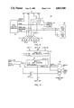
- FIG. 1 shows a parallel processing system 20 which consists of an arrangement of data processing elements 26 through 59 connected to a host computer 22.
- the data processing elements 26 through 59 are arranged in a binary tree and the processing system 20 of FIG. 1 includes 31 individual data processing elements.
- the root data processing element 26 is connected to host computer 22 through a host interface 24.
- the processing elements 26 through 59 are arranged in a binary tree with processing element 26 at what will be called the "root” or highest order position of the tree and processing elements 44 through 59 at the "leaves" or lowest order position of the tree.
- the data processing system may use any size binary tree, and a prototype system has been constructed with 1,023 identical processing elements arranged in such a binary tree.
- This prototype system uses a VAX 11/750 computer as a host.
- a typical element in the binary tree, such as data processing element 32 has a higher order parent data processing element in the tree i.e. data processing element 29 and two lower order child data processing elements 36, 37.
- the lower order data processing elements 36, 37 will be referred to herein respectively as the left child and right child data processing elements.
- data processing element 36 is the left child of data processing element 32
- data processing element 37 is the right child of data processing element 32.
- Data processing element 29 is the parent of data processing element 32.
- the binary tree 20 as illustrated in FIG. 1 includes sub-sets which are also binary trees. Accordingly, there is a binary tree with data processing element 32 as its root, which includes data processing elements 36, 37 and 44 through 47. Likewise a binary tree is formed with data processing element 33 as a root, and includes data processing elements 38, 39 and 48 through 51. This arrangement enables variations in the data processing operations wherein the sub-binary trees of binary tree 20 may act separately as separate processing systems acting in parallel.
- the present invention contemplates identical data processing elements, independent of their location within the binary tree. This facilitates easy construction, interconnection and replacement of the data processing elements.
- the system of the present invention provides significantly reduced “overhead” processing time for these functions.
- the method contemplated by the present invention provides for identical construction, wiring and programming of the data processing elements in the system, to render them interchangeable, and still provide the capability for unique programming of the individual data processing elements.
- FIG. 2 illustrates in greater detail the interconnection of data processing elements 26 and 29 through 35 of the processing system 20.
- Each of the data processing elements includes a central processing unit 60 and an interface unit 61.
- the central processing unit includes a one chip microcomputer and a selected amount of read only memory and random access memory.
- the read only memory includes a program, which shall be referred to as the "kernel" program, which provides for initialization and overall operation of the processing unit in each data processing element.
- the random access memory associated with each of the processing elements provides memory space for program instructions and program data required for the data processing operation to be performed.
- the interface unit 61 is of special design and is described in detail in commonly owned copending application Ser. No.
- Interface unit 61 includes a series of registers and logic elements for performing certain functions pertinent to the methods of this invention. Certain of the registers of interface unit 61 are memory mapped for transfer of instructions and/or data and control signals to and from central processing unit 60 and its associated memory.
- a significant feature of the processing system 20 is the fact that there are two independent connections between each of the data processing elements and its parent and child data processing elements. Accordingly as illustrated in FIG. 2 data processing element 29 has a connection from its interface unit 61 to the interface unit of its parent data processing element 26. Likewise interface unit 61 of data processing element 29 is connected to the interface unit 61 of its left child data processing element 32 and its right child data processing element 33.
- the interconnection between the interface units 61 is a register-to-register interconnection which provides for a rapid "broadcast” operation and a "resolve/report” operation in accordance with the present invention, both of which will be further described in detail.
- central processing units 60 of each of the data processing elements in the processing system 20 are interconnected with the central processing units in the parent and child data processing elements as illustrated in FIG. 2. Accordingly central processing unit 60 of data processing element 29 is connected to the identical central processing unit 60 of data processing element 26 and to the central processing unit 60 of its left child data processing element 32 and right child data processing element 33.
- FIG. 3 shows in somewhat greater detail a block diagram of a single data processing element 29 useful in the processing system 20 of the present invention.
- the data processing element 29 includes interface unit 61 which is an input/output chip of special design as described in the aforementioned copending application.
- a single chip computer 64 which in this case is an 8751 processor.
- a parity memory 66 comprising 64K1 S-RAM, is provided and 16K random access memory 68 consisting of two 8K ⁇ 8 S-RAM chips is also provided as a working memory for the single chip computer 64.
- Computer 64 with its associated memories forms central processing unit 60.
- terminals A, B, C, and D by which data processing element 29 is connected to its parent and child data processing elements. Accordingly there are shown four terminals A, B, C, and D at connection 70 for connection between data processing element 29 and its parent data processing element 26. Likewise, four terminals A, B, C, and D are provided at connection 72 for connection to left child data processing element 32 and four terminals A, B, C, and D are provided at connection 74 for connection to right child data processing element 33. It should be understood that the terminals A, B, C, and D may each include one or more pin interconnections.
- a parallel port, labeled "parent port” of 8751 computer 64 is connected through 8 pin terminal 70A to terminal 72A of the parent data processing element and thus to the address/data port of the single chip computer 64 in the parent data processing element.
- Terminals B at each connection is used to provide handshake status lines between the computers in the adjacent data processing elements.
- Terminals C of connections 70, 72 and 74 are used to provide data interconnection between the interface input/output chips 61 in the parent and child data processing elements and terminals D are used to provide by control connections between the input/output chip 61 in the parent and child data processing elements in the binary tree.
- FIGS. 2 and 3 under which data processing elements are coupled to their parent and child data processing elements by interconnections through the interface unit 61 and by direct connections of the central processing units 60 provides multiple capability for communications on the binary tree.
- the interface unit 61 are primarily used.
- the arrangement of the interface unit 61 for the downward communication from the host computer is by means of coupled registers and serial data streams which provide relatively rapid communications in the binary tree without operation of the central processing units 60 except for loading of data into memory.
- the process of downward communication in the binary tree is herein referred to as the "broadcast" operation.
- the broadcast operation can originate at the host computer, the root processing element 26 or one of the lower order data processing elements to provide multiple parallel operation using different parts of the binary tree. It is possible, for example, to simultaneously broadcast instructions or data from data processing elements 32, 33, 34 and 35 to the sub-binary trees formed of data processing elements connected respectively below these data processing elements for purposes, for example, of providing redundant calculations to assure accuracy or for purposes of doing parallel computations on different data sets simultaneously.
- each data processing element can function independent of its parent data processing element or in an operation which requires constant connection to its parent element.
- the data processing element can act as a root element for a sub-binary tree formed by the lower order data processing elements connected below it.
- One form of data processing operation contemplated for the processing system 20 is classified as a "membership" problem.
- This problem is a form of decomposable searching problems wherein the system must answer inquiries of whether an object X is included in a set of objects F.
- the system would provide each data processing element with a set of instructions and a set of program data which comprises an arbitrary subset of F.
- the system can then operate by providing the unknown operating data X to all the data processing elements to compare data X with its own subset of F.
- the results of these comparisons are then provided to the root data processing element and reported to the host.
- the system can provide a series of such operations on a set of unknown data X 1 , X 2 , . . . etc.
- a similar form of decomposable searching problem is to compare an unknown point to a set of points to find which point is the nearest neighbor.
- the data representing the set of points can be distributed to the data processing elements and for each unknown point X 1 , X 2 etc. the data processing elements compute the distance to the data points subset stored in the local memory.
- the data processing elements operate in a single instruction multiple data (SIMD) mode, wherein the data processing elements contain multiple subsets of the data set F and each operate on the same instruction (compare X to F).
- SIMD single instruction multiple data
- the data processing elements remain logically connected to the root data processing element to receive inquires (as simple instructions or unknown data) and to report the results of the data processing operation.
- MIMD multiple instruction, multiple data
- a data processing element operating in the MIMD mode can act as a root data processing element for its lower order descendants which will then operate in the SIMD mode.
- the broadcast operation originates in host interface 24 or in a higher order data processing element operating in the MIMD mode.
- the portions of the interface unit illustrated in FIG. 4 include, a broadcast output shift register 72, a broadcast multiplexer 74, AND gate 76, broadcast input shift register 78, flip-flop 80 and AND gate 82.
- clock signals are continually being supplied to broadcast out shift register 72.
- the serial input to this shift register is tied to a "one" condition so that the shift register is constantly providing an output of ones at its serial output port.
- the data is loaded into the broadcast out shift register as a parallel 8 bit byte.
- a parity bit and a start bit consisting of a "zero" are loaded with the data byte.
- the shift register then shifts out a data stream consisting of the start bit, 8 bits of data and the parity bit through the serial output port to multiplexer 74. Since the data processing element must be operated in the MIMD mode, multiplexer 74 is connected to provide the output of shift register 72 to the serial data output and thereafter to the lower order data processing elements.
- the signals supplied to the serial data in AND gate 76 are disconnected so that the data processing element does not respond to broadcast signals from its ancestors.
- the broadcast-out shift register 72 is not loaded with a data byte until the data processing element received "ready" signals from its left child and right child. As will be indicated below, these signals are not provided until all lower order data processing elements signal a "ready" condition.
- the serial data is supplied to the serial data input port of AND gate 76.
- These processing elements must be operating in the SIMD mode to receive broadcast data from their parent data processing element, and accordingly the upper input to AND gate 76 is in a "one" condition, and the serial input data stream is provided to broadcast-in shift register 78 in serial form.
- the input data stream Prior to a broadcast the input data stream is a series of "ones" originating in the serial input port of the broadcast-out shift register 72 originating the broadcast. Accordingly the last bit in the shift register 78 prior to reception of a data byte is in a "one" condition, and the shift enable of a broadcast-in shift register 78 is in an enabled condition.
- the shift enable signal goes to a zero condition and shift register 78 is fully loaded and shifting is stopped.
- the zero start bit is also supplied to AND gate 82 which disables the ready signal provided to the parent data processing element.
- the data processing element originating the broadcast will not transmit another stream of data until it receives a ready signal from AND gate 82 of its two child processing elements.
- serial data stream from the output of AND gate 76 is also provided to flip-flop 80 which provides a one clock pulse delay in the data stream prior to supplying the data stream to output multiplexer 74. Since the data processing elements receiving broadcast data are in the SIMD mode, the serial data stream from D flip-flop 80 will be provided to the output of multiplexer 74 for transmission to lower order data processing elements. The data stream therefore suffers a one clock pulse delay for each order of data processing elements through which it passes.
- the register contents may be transferred as data to the data processing element or its memory in parallel form.
- "ones” are loaded into the broadcast-in shift register 78 to change the start bit position to a "one”, thereby re-enabling the shift enable of register 78 and providing a ready signal to be transmitted upward to the parent data processing element through AND gate 82.
- the ready signal is not transmitted until ready signals are received from the child elements of each individual data processing element. Accordingly a ready signal is conveyed up to the MIMD root data processing element only after the data byte has been transmitted and shifted into all of the data processing elements in the binary tree.
- the arrangement of the broadcast registers as illustrated in FIG. 4 provides a relatively small, one clock pulse, delay between transfer of data for each stage of the binary tree. All of the data processing elements operate on the same clock at a rate of about 12 MHz.
- the arrangement enables changing of the data processing element from the SIMD to the MIMD mode, so that groups of data processing elements can be disconnected from their parent data processing elements for independent and simultaneous operation, individually or with their own lower order elements in sub-trees of multiple data processing elements.
- Another important functional aspect of the processing system of the present invention is the resolve and report operation.
- the host processor would provide data to be processed, in the broadcast mode, to all of the data processing elements for simultaneous processing.
- the data to be processed may be, for example, an unknown signal (such as voice) in digitized form which is to be compared to known signal samples (templates) which are stored as program data in the various data processing elements of the binary tree.
- templates known signal samples
- the results in the data processing elements are compared to each other while they are passed up to the root of the binary tree through the registers in the interface units.
- the interface units in the first higher order level of system 20, comprising data processing elements 36 through 43 would each compare the results reached in their respective central processing units with the results reached in their child data processing elements.
- the interface registers of data processing element 36 compares the result from its own central processing unit with the results reached in data processing elements 44 and 45.
- the interface unit of data processing element 37 compares the results reached by its own central processing unit with the results reached by data processing elements 46 and 47.
- the next step of resolve the interface units in data processing elements at the next higher level would again compare their own result with the results reached by the lower order data processing elements.
- the resolve function In this step the most favorable results reached in the lowest and second lowest level data processing elements are provided by data processing elements 36 and 37 to data processing element 32 for comparison with the result reached in that data processing element.
- the resolve continues until the best result in all of the data processing elements reached in the binary tree is reported to the host processor.
- the resolve function additionally provides signals to be generated for each data processing element, which indicates whether that data processing element is the one which has generated the most favorable value. This signal is called the "kill" signal for convenience and results in the killing or inactivation of all processing elements except the one processing element which has provided the winning value.
- the winning value may be a maximum value, a minimum value or any other criteria which can be easily determined in a register.
- the logic circuitry used for the resolve operation which is built into the interface unit, has a selected order for resolution of equal result values.
- the resolve operation is not only used for reporting the results of the calculation, but as will be further described, is also used for purposes of enumerating the processing elements and identifying processing elements which are to receive individual processing element instructions during a broadcast operation.
- FIG. 5 is a block diagram showing portions of the interface unit which are used in connection with the resolve operation.
- the block diagram of FIG. 5 shows input registers 84, 86 and 88.
- Input register 84 is connected to receive the result of a calculation or other data transferred from the central processing unit associated with the particular interface unit containing the illustrated registers.
- Register 86 and 88 are connected respectively to receive the output value from the left child and the right child data processing elements.
- a serial comparator and state controller 90 is provided to compare the values in registers 84, 86 and 88 in a bit-by-bit serial comparison with the most significant data bit being compared first.
- a typical comparison is to determine the maximum or minimum value of the three values in registers 84, 86 and 88.
- serial comparator additionally contains circuitry arrangements to resolve ties in the values as will be further described.
- Serial comparator and state controller 90 generates kill signals according to the comparison values and also controls multiplexer 92 to transfer the most favorable value to the output register 94 and the parent processing element.
- the most favorable value is a maximum value of a particular calculation which has been performed by all of the data processing elements using data stored in those data processing elements. For example, there might be a correlation calculation between supplied unknown data X and data F stored at each processing element. The value which results would be maximum for maximum correlation of the unknown data with the data stored in each data processing element. Assume that the processing element associated with the register shown in FIG. 5 has developed a value of 10, the left child has developed a value of 8 and the right child has developed a value of 5. In this situation the serial comparator 90, upon comparing these values would determine that the processing element associated with that interface unit has won the comparison, and it would generate signals to the left child and the right child to "kill" those processing elements for purposes of this resolve operation.
- KL and KR signals are indicated as the KL and KR signals.
- the KS (kill self) signal would not be generated in this case.
- Multiplexer 92 is then controlled to pass the winning value stored in register 84 to output register 94 and to transfer that value to one of the input fifo registers in the parent processing element for further comparison.
- a kill signal is generated by the parent and provided to serial comparator and state controller 90 as signal KP.
- serial comparator and state controller 90 must receive go ahead signals from its left child and right child data processing elements and its own central processing unit to indicate that computations have been completed and the values to be compared have been stored in input registers 84, 86 and 88.
- state controller 90 provides a go signal to its parent processing element to continue the resolve operation at a higher level.
- FIG. 6 illustrates a typical resolve operation which compares resulting numbers in various data processing elements of a small binary tree to determine the maximum value computed.
- the values generated for each of the data processing elements PE1 to PE7 are indicated in the processing element boxes.
- the illustration is for a relatively small binary tree of 7 processing elements, but illustrates the manner in which the resolve operation takes place.
- a first comparison takes place in processing element PE2 to compare the results reached in PE1, PE2 and PE3.
- the results of this comparison indicate that PE3 is the winning processing element and accordingly a KL signal is sent to PE1 to deactivate that processing element and a KS signal is generated to deactivate processing element PE2.
- Simultaneously PE6 does a comparison of the results reached in PE5, PE6 and PE7.
- a KL signal is generated to deactivate PE5 in a KS signal is generated to deactivate PE6.
- the maximum value results reached in PE2 and PE6 are forwarded to PE4 for a final comparison.
- a KS signal is generated to deactivate PE4 and a KL signal is generated and passed to PE2.
- the KL sent to PE2 is passed on by PE2 to deactivate PE3.
- PE7 which contains the winning value of 8
- the result of the computation, "8" which is the maximum value determined, is placed in the output register of PE4.
- FIG. 7 illustrates the manner in which the resolve operation handles ties in the output register values of the various processing elements.
- each of the processing elements has an output value of "one" in its output register thereby making a tie of all the processing elements.
- This type of resolve operation with identical values is used in connection with the processing system for purposes of enumerating the various identical processing elements.
- the first resolve operation takes place in PE2.
- the logic of PE2 causes it to favor its left child in the event in a three-way tie and to favor itself over its right child. Accordingly, PE2 generates KS and K signals to deactivate PE2 and PE3. Likewise, processing PE6 generates KS and KR signals to resolve the tie in favor of its left child PE5.
- PE4 viewing the equal results passed on by PE2 and PE6 generates a KS and a KR signal.
- the KS signal deactivates PE4 and the KR signal is passed down by PE6 to deactivate PE5. Accordingly, the result of the tie resolve operation illustrated causes deactivation of all processing elements except PE1.
- the tie resolution operation illustrated in FIG. 7 can be used in connection with supplying individual programs to the various data processing elements. Following the operation illustrated in FIG. 7 all data processing elements except PE1 have received a kill signal and are in an inactivated state. Signals representing program instructions and/or data which are intended to be provided only to PE1 may then be broadcast from the host interface. Since PE1 is the only active data processing element, only PE1 will operate to transfer these signals to its local memory. The individual instructions, once loaded, can be operated to cause PE1 to place its resolve out register in the zero condition. The resolve operation is then repeated and PE1 will be deactivated, since it has a zero condition output. On the second resolve operation all elements except PE2 will be deactivated. This process can be continued until the processing elements are supplied with individual program instructions and data in the order illustrated in FIG. 8. Set forth below are the logical equations used by each processing element in the resolve operation for maximum value:
- FIG. 9 is a series of diagrams 9A through 9L which illustrate the operation of the data processing system of the present invention to perform a computation which involves parallel processing. It is assumed that the operation is of a type wherein each of the processing elements is provided with program instructions which are identical for all elements and also provided with program instructions and/or program data which are different for each of the processing elements.
- a program of this sort may involve, for example, analyzing signal samples of voice, acoustic, X-ray or radar signals, to compare the signal sample to signal samples associated with known parameters. For example, it may be desired to examine the signal characteristics of digitized voice signals to compare those signals with the signal characteristics known to be representative of various words (called templates).
- each of the processing elements is provided with instructions for performing the comparison and each of the processing elements would be provided with a portion of the data bank (templates) which is to be used for comparison.
- data processing takes place as unknown signal information is provided from the host computer to the binary tree of data processing elements for simultaneous data processing on the unknown data in each of the data processing elements, using the individual program data resident in the data processing elements.
- the type of operation above described may be characterized as a "decomposable searching problem" wherein the known data can be decomposed into arbitrary subsets of known data, one or more of which is provided to each of the processing elements and therein compared against the unknown data.
- the system of the present invention is particularly adapted to such a decomposable searching problem, but more important is also adapted to perform what the inventor characterizes as a "almost decomposable searching problem" wherein a series of searching operations are used to compare the unknown data to known data, but the content or the approach to the comparison is changed in a subsequent data comparison operation. The change in the subsequent data comparison operation is dependent on the result of earlier operations.
- the letter C represents common program instructions (and possibly program data) which is identical in each of the data processing elements in the binary tree of data processing elements.
- the designation D i is used in connection with data or program instructions which are individual to each of the processing elements in the system.
- the combination of C and D i constitutes the program and program data for each processing element.
- the data D i may represent templates representative of words to be recognized by the system.
- the common program C would represent the algorithm by which unknown data is compared to the templates.
- a designation M is used in connection with unknown data, which must be compared to the known data D resident in each of the data processing elements.
- the letter K is used for the processing element kill signal, which has been discussed in connection with the resolve operation and the letter R is used to designate the output register value which is used in the resolve operation.
- each of the data processing elements Prior to operation of the system each of the data processing elements includes read only memory on which there is resident a set of kernel instructions, which are used for the initialization of the data processing element after power and clock pulses are supplied to the system and also used in connection with loading of the program instructions and data.
- the system causes the initialization of each of the data processing elements and the kernel element is run.
- the kernel program the data processing elements and their respective interface units are prepared to receive and execute program instructions which follow in the broadcast mode from the host computer.
- Step 2 shows the initial broadcast of common program instructions and common program data from the host computer into the binary tree of data processing elements. At this point all of the data processing elements are active and all of the processing elements receive and load this common program and common data. As a result of either the common program or the resident kernel software each of the data processing elements sets it output register for the resolve operation to a predetermined condition, for example, hexidecimal FF as illustrated in FIG. 9B.
- Step 3 shown in FIG. 9C is the first resolve operation. As previously discussed ties are resolved such that PE1 is the only data processing element not placed in the "kill" condition. The other data processing elements are thereby operating but not responsive to signals broadcast from the root, and they do not load these signals or change their condition. Accordingly after the resolve operation of step 3 only PE1 is in condition to receive and load additional program instructions and/or data.
- Step 4 illustrates the loading of additional program instructions and data into PE1.
- the program instructions and/or data D1 are broadcast as signals from the root in a manner identical to the broadcast of the common program instructions and data, except that only processing element PE1 is in a condition to load the signals.
- Step 5 illustrated in FIG. 9E shows a resolve operation which takes place following the loading of signals D1 in PE1. In this resolve operation all elements are killed except processing element PE2. Signals D2 to be loaded in PE2 are broadcast and loaded in PE2 as shown in step 6 in FIG. 9F.
- Step 7 in FIG. 9G shows the condition of the processing elements in the binary tree after the loading of data D2 in data processing element PE2.
- Step 8 shows the condition of the data processing system after all of the processing elements have been loaded with the common program instructions and data C and the individual program instructions and data D1 through D7. At this step each of the output registers of the data processing elements has been placed in the zero condition and the machine is ready to receive either instructions for operations to be performed on the data or data to be processed in accordance with the instructions contained in each of the elements.
- Step 9 shows further operation of the data processing system where actual data processing takes place.
- Unknown information to be processed indicated by M1 is broadcast from the host computer through the host interface to all of the data processing elements.
- each of the data processing elements compares unknown data M1 to the stored data in its individual memory. This comparison takes place simultaneously in the various processing elements, and therefore a large number of comparisons can take place at once.
- the broadcast arrangement of coupled registers by which the unknown signal M is supplied to the processing elements through registers eliminates significant "overhead" time delay in sending the unknown information to the data processing elements for processing.
- each of the processing elements places some indication of the results of the processing in its output register. As illustrated in FIG.
- each of the processing elements after comparing unknown data M1 to the contents of its data memories D1 through D7 reach a result of either "yes" or "no".
- a negative result in the illustrated example causes the output register R to be placed in a zero condition.
- An affirmative caused the output register R to be placed in the "one" condition.
- processing element PE5 has its output register placed in the one condition showing a match between unknown data M1 and stored data D5.
- the illustrated example shows an identical match between data, but it is also possible that the comparison instructions find the degree of match, for example, between samples of an unknown voice signal which is broadcast as a sequence of data M1, and templates of known signals representing words which are stored in memory as a sequence of samples comprising data D1 through D7.
- the results in this type of operation may be correlation value, wherein the correlation values vary according to the degree of correlation between the unknown signal and the various known signals.
- the value placed in each output register can represent the degree of correlation.
- the output register can be set to zero if there is no identical match between the unknown data M1 and the known data D1 to D7, and the output register would be set to an identifying number, which is not equal to zero, when the unknown data M1 matches some part of the known data.
- the identifying number identifies what portion of the data register, for example D4, correlates with the unknown data M1.
- a resolve operation is performed, as shown in FIG. 9J.
- all of the processing elements except element PE5 are caused to be killed by the resolve operation, since all have their output register set to zero, except element PE5, which is set to one.
- processing element PE5 which is provided to the root would be the "one", which originated in processing element PE 4 and is passed upward during the resolve operation.
- This "one" signal indicates to the host computer that there has been an identical match in at least one of the processing elements, but the host has no indication which data processing element corresponds to the match or what portion of the data the match represents.
- a further step is required. In the event none of the processing elements found a match in its data memory the resolve operation would result in a zero being reported to the host computer representing that none of the data in the data memory bank correlated with the unknown data.
- Step 11 in FIG. 9K shows a "report" operation being performed.
- the report may automatically take place by the relaying of the register value through the binary tree during the resolve operation. This register value may be sufficient for the operation being performed.
- it may be desirable to find out additional information about the results of the calculation for example, the specific value of a correlation function and the identity of the data with which correlation has been identified as being most favorable.
- further steps in the data processing element instructions may cause the output register of the processing element PE5 which has not been killed and which has the most favorable result to be placed in a condition which would report that result.
- step 11 the output register of processing element PE5 has been placed in a condition identified as D4 to represent an identification or report of the correlation results which is to be relayed to the host computer.
- a resolve operation is repeated and this report as a most favorable value compared to ⁇ is passed upwardly through the resolve registers to the host computer as illustrated in FIG. 9K.
- FIG. 10 is a program flow diagram showing steps 1 through 11 illustrated in FIG. 9 and alternative operations for step 12 for a production system.
- the modification can be implemented by broadcasting instructions (step 12A, FIG. 10) for the modification to all data processing elements and causing the elements to simultaneously execute those instructions to modify the previously existing common program instructions C and individual program instructions or data D.
- the changes can be individually broadcast to the data processing elements by the enumeration and broadcast operation of steps 3 to 8 as described above. (Step 12B, FIG. 10). If the modification involves only the "winning" data processing element, modifications to the instructions and data in that processing element can be broadcast before clearing the kill signals of the previous operation.
- Step 12C it is also possible to "direct" modification signals to less than all the data processing elements by instructing a specific data processing element to identify itself in the resolve register.
- the original individual data Di would include unique identification data to be loaded in each data processing element memory.
- the host can broadcast instructions to compare a broadcast number (corresponding to the desired data processing element) with the stored identification data and put the correlation output in the resolve register. The resolve operation will then disable all but the desired data processing element, which can then be loaded with instructions or data signals.
- the system of the invention has been described with reference to applications wherein all data processing elements have different instructions and program data combinations. In some applications it may be desirable to provide identical program instructions and data to two or more data processing elements to provide redundancy for fault identification. This can be achieved by use of the MIMD/SIMD modes to sub-divide system 20 of FIG. 1 into sub-binary trees.
- system 20 of FIG. 1 can be divided into four binary sub-trees with data processing elements 32, 33, 34 and 35 acting as root processing elements of the subtrees.
- Each of the data processing elements of each sub-tree must be loaded with program instructions and data. Common instructions can be broadcast from interface 24 and stored in all elements. Individual instructions and program data for the sub-tree can be loaded by the usual sequence, or can be simultaneously loaded in each sub-tree.
- the lower order data processing elements can be loaded by performing a resolve operation of the sub-trees in the MIMD mode, to inactivate all but one data processing element in each sub-tree (i.e., PE44, PE48, PE52 and PE56).
- the root element may then return to SIMD mode and pass instructions and/or data broadcast from host 22 for simultaneous loading in the four active data processing elements in each sub-tree.
- the sub-tree root elements can return to MIMD state to select and load the next data processing element in each sub-tree.
- the selection and loading of the data processing elements in each sub-tree by its respective sub-tree root element is carried out with each sub-tree operating independently in SIMD state.
- Parallel operation can be performed on data broadcast from the host with the sub-tree root elements in SIMD state and individual resolve/report operations can be performed with the root elements in MIMD state.
- Data processing elements 26, 29 and 30 can compare the results in the parallel operation and provide them to the host.
- the data processing elements in the binary tree are interconnected between the central processing units as well as through the interface registers used for broadcast and resolve/report operation.
- the interface registers provide the most efficient means to provide signals to the data processing elements and obtain the results of their operations.
- the broadcast and resolve/report operations can take place rapidly in a single instruction cycle of the machine and thus reduce significantly the machine time "overhead".
- the higher level data processing elements receive instructions to read the resultant values reached by their child elements and combine those results. These results are passed by the direct connections between the central processing units. Likewise, the higher order data processing elements can directly pass instructions or data to their lower order data processing elements by this connection.
Abstract
Description
VP=Maximum (VS, VL, VR)
KL=KP OR (VS>VL) OR (VR>VL)
KR=KP OR (VS>=VR) OR (VL>VR)
KS=KP OR (VS<=VL) OR (VS<VR)
Claims (7)
Priority Applications (10)
| Application Number | Priority Date | Filing Date | Title |
|---|---|---|---|
| US06/903,031 US4843540A (en) | 1986-09-02 | 1986-09-02 | Parallel processing method |
| AU79693/87A AU598877B2 (en) | 1986-09-02 | 1987-08-27 | Parallel processing method |
| DE3751205T DE3751205T2 (en) | 1986-09-02 | 1987-08-27 | PARALLEL PROCESSING SYSTEM AND METHOD FOR USE THEREOF. |
| KR1019880700483A KR930006383B1 (en) | 1986-09-02 | 1987-08-27 | Paralell processing method |
| AT87906244T ATE120573T1 (en) | 1986-09-02 | 1987-08-27 | PARALLEL PROCESSING SYSTEM AND METHOD FOR USE THEREOF. |
| JP62505660A JP2788727B2 (en) | 1986-09-02 | 1987-08-27 | Parallel processing system and method of use |
| PCT/US1987/002106 WO1988001769A1 (en) | 1986-09-02 | 1987-08-27 | Parallel processing system and method of using the same |
| EP87906244A EP0280723B1 (en) | 1986-09-02 | 1987-08-27 | Parallel processing system and method of using the same |
| CA000545781A CA1289262C (en) | 1986-09-02 | 1987-08-31 | Parallel processing method |
| IL83733A IL83733A (en) | 1986-09-02 | 1987-09-02 | Parallel processing system |
Applications Claiming Priority (1)
| Application Number | Priority Date | Filing Date | Title |
|---|---|---|---|
| US06/903,031 US4843540A (en) | 1986-09-02 | 1986-09-02 | Parallel processing method |
Publications (1)
| Publication Number | Publication Date |
|---|---|
| US4843540A true US4843540A (en) | 1989-06-27 |
Family
ID=25416823
Family Applications (1)
| Application Number | Title | Priority Date | Filing Date |
|---|---|---|---|
| US06/903,031 Expired - Lifetime US4843540A (en) | 1986-09-02 | 1986-09-02 | Parallel processing method |
Country Status (10)
| Country | Link |
|---|---|
| US (1) | US4843540A (en) |
| EP (1) | EP0280723B1 (en) |
| JP (1) | JP2788727B2 (en) |
| KR (1) | KR930006383B1 (en) |
| AT (1) | ATE120573T1 (en) |
| AU (1) | AU598877B2 (en) |
| CA (1) | CA1289262C (en) |
| DE (1) | DE3751205T2 (en) |
| IL (1) | IL83733A (en) |
| WO (1) | WO1988001769A1 (en) |
Cited By (60)
| Publication number | Priority date | Publication date | Assignee | Title |
|---|---|---|---|---|
| US5305462A (en) * | 1986-09-18 | 1994-04-19 | Digital Equipment Corporation | Mechanism for broadcasting data in a massively parallell array processing system |
| US5410654A (en) * | 1991-07-22 | 1995-04-25 | International Business Machines Corporation | Interface with address decoder for selectively generating first and second address and control signals respectively in response to received address and control signals |
| US5434972A (en) * | 1991-01-11 | 1995-07-18 | Gec-Marconi Limited | Network for determining route through nodes by directing searching path signal arriving at one port of node to another port receiving free path signal |
| GB2252185B (en) * | 1991-01-18 | 1995-08-02 | Kenneth Wayne Iobst | Apparatus for processing data from memory and from other processors |
| US5440689A (en) * | 1991-12-12 | 1995-08-08 | International Business Machines Corporation | Interprocessor communication system for direct processor to processor communication between internal general purpose registers transparent to the execution of processors thereof |
| US5452461A (en) * | 1989-04-28 | 1995-09-19 | Hitachi, Ltd. | Program parallelizing apparatus capable of optimizing processing time |
| US5485612A (en) * | 1991-02-13 | 1996-01-16 | Hitachi, Ltd. | Method and apparatus for assigning processors in parallel computer system |
| US5513371A (en) * | 1992-01-07 | 1996-04-30 | International Business Machines Corporation | Hierarchical interconnection network architecture for parallel processing, having interconnections between bit-addressible nodes based on address bit permutations |
| US5522083A (en) * | 1989-11-17 | 1996-05-28 | Texas Instruments Incorporated | Reconfigurable multi-processor operating in SIMD mode with one processor fetching instructions for use by remaining processors |
| US5748780A (en) * | 1994-04-07 | 1998-05-05 | Stolfo; Salvatore J. | Method and apparatus for imaging, image processing and data compression |
| US5748967A (en) * | 1993-01-11 | 1998-05-05 | Hitachi, Ltd. | Program rewriting method and apparatus for multiprocessor system |
| US5848402A (en) * | 1994-07-07 | 1998-12-08 | Ai Ware, Inc. | Universal system for artificial intelligence based learning, categorization, and optimization |
| US5937194A (en) * | 1997-03-12 | 1999-08-10 | International Business Machines Corporation | Method of, system for, and article of manufacture for providing a generic reduction object for data parallelism |
| US5978831A (en) * | 1991-03-07 | 1999-11-02 | Lucent Technologies Inc. | Synchronous multiprocessor using tasks directly proportional in size to the individual processors rates |
| US5987255A (en) * | 1997-03-12 | 1999-11-16 | International Business Machines Corporation | Method of, system for, and article of manufacture for providing a generic adaptor for converting from a sequential iterator to a pre-thread parallel iterator |
| US5991764A (en) * | 1997-03-12 | 1999-11-23 | International Business Machines Corporation | Data structure specifying differing fan-in tree and fan-out tree computation patterns supporting a generic reduction object for data parallelism |
| US6000024A (en) * | 1997-10-15 | 1999-12-07 | Fifth Generation Computer Corporation | Parallel computing system |
| US6061730A (en) * | 1995-11-13 | 2000-05-09 | Billings; Roger E. | Methods and apparatus for communicating data in computer networks with separate packet assembly and packet broadcast channels |
| US6219717B1 (en) | 1996-11-20 | 2001-04-17 | Merrill Lynch & Co., Inc. | Method and apparatus for implementing object transparent invocation |
| US6237134B1 (en) | 1997-03-12 | 2001-05-22 | International Business Machines Corporation | Method of, system for, and article of manufacture for providing a generic adaptor for converting from a non-future function pointer to a future function object |
| US20050027455A1 (en) * | 2003-08-01 | 2005-02-03 | Moac Llc | Systems and methods for geophysical imaging using amorphous computational processing |
| US20050138622A1 (en) * | 2003-12-18 | 2005-06-23 | Mcalpine Gary L. | Apparatus and method for parallel processing of network data on a single processing thread |
| US20080022079A1 (en) * | 2006-07-24 | 2008-01-24 | Archer Charles J | Executing an allgather operation with an alltoallv operation in a parallel computer |
| US20080028463A1 (en) * | 2005-10-27 | 2008-01-31 | Damballa, Inc. | Method and system for detecting and responding to attacking networks |
| US20080301683A1 (en) * | 2007-05-29 | 2008-12-04 | Archer Charles J | Performing an Allreduce Operation Using Shared Memory |
| US20090079466A1 (en) * | 2007-09-22 | 2009-03-26 | Hirak Mitra | Soft-reconfigurable massively parallel architecture and programming system |
| US20090240915A1 (en) * | 2008-03-24 | 2009-09-24 | International Business Machines Corporation | Broadcasting Collective Operation Contributions Throughout A Parallel Computer |
| US20090245134A1 (en) * | 2008-04-01 | 2009-10-01 | International Business Machines Corporation | Broadcasting A Message In A Parallel Computer |
| US20090292905A1 (en) * | 2008-05-21 | 2009-11-26 | International Business Machines Corporation | Performing An Allreduce Operation On A Plurality Of Compute Nodes Of A Parallel Computer |
| US20090307467A1 (en) * | 2008-05-21 | 2009-12-10 | International Business Machines Corporation | Performing An Allreduce Operation On A Plurality Of Compute Nodes Of A Parallel Computer |
| US20100017420A1 (en) * | 2008-07-21 | 2010-01-21 | International Business Machines Corporation | Performing An All-To-All Data Exchange On A Plurality Of Data Buffers By Performing Swap Operations |
| US20100037314A1 (en) * | 2008-08-11 | 2010-02-11 | Perdisci Roberto | Method and system for detecting malicious and/or botnet-related domain names |
| US20100274997A1 (en) * | 2007-05-29 | 2010-10-28 | Archer Charles J | Executing a Gather Operation on a Parallel Computer |
| US20110047349A1 (en) * | 2009-08-18 | 2011-02-24 | Kabushiki Kaisha Toshiba | Processor and processor control method |
| US20110167495A1 (en) * | 2010-01-06 | 2011-07-07 | Antonakakis Emmanouil | Method and system for detecting malware |
| US7991857B2 (en) | 2008-03-24 | 2011-08-02 | International Business Machines Corporation | Broadcasting a message in a parallel computer |
| US20110238950A1 (en) * | 2010-03-29 | 2011-09-29 | International Business Machines Corporation | Performing A Scatterv Operation On A Hierarchical Tree Network Optimized For Collective Operations |
| US8332460B2 (en) | 2010-04-14 | 2012-12-11 | International Business Machines Corporation | Performing a local reduction operation on a parallel computer |
| US8346883B2 (en) | 2010-05-19 | 2013-01-01 | International Business Machines Corporation | Effecting hardware acceleration of broadcast operations in a parallel computer |
| US8484440B2 (en) | 2008-05-21 | 2013-07-09 | International Business Machines Corporation | Performing an allreduce operation on a plurality of compute nodes of a parallel computer |
| US8489859B2 (en) | 2010-05-28 | 2013-07-16 | International Business Machines Corporation | Performing a deterministic reduction operation in a compute node organized into a branched tree topology |
| US20130185381A1 (en) * | 2012-01-17 | 2013-07-18 | International Business Machines Corporation | Configuring Compute Nodes In A Parallel Computer Using Remote Direct Memory Access ('RDMA') |
| US8566841B2 (en) | 2010-11-10 | 2013-10-22 | International Business Machines Corporation | Processing communications events in parallel active messaging interface by awakening thread from wait state |
| US8631489B2 (en) | 2011-02-01 | 2014-01-14 | Damballa, Inc. | Method and system for detecting malicious domain names at an upper DNS hierarchy |
| US8756612B2 (en) | 2010-09-14 | 2014-06-17 | International Business Machines Corporation | Send-side matching of data communications messages |
| US8826438B2 (en) | 2010-01-19 | 2014-09-02 | Damballa, Inc. | Method and system for network-based detecting of malware from behavioral clustering |
| US8893083B2 (en) | 2011-08-09 | 2014-11-18 | International Business Machines Coporation | Collective operation protocol selection in a parallel computer |
| US8910178B2 (en) | 2011-08-10 | 2014-12-09 | International Business Machines Corporation | Performing a global barrier operation in a parallel computer |
| US8949577B2 (en) | 2010-05-28 | 2015-02-03 | International Business Machines Corporation | Performing a deterministic reduction operation in a parallel computer |
| US9166994B2 (en) | 2012-08-31 | 2015-10-20 | Damballa, Inc. | Automation discovery to identify malicious activity |
| US9330060B1 (en) * | 2003-04-15 | 2016-05-03 | Nvidia Corporation | Method and device for encoding and decoding video image data |
| US9424087B2 (en) | 2010-04-29 | 2016-08-23 | International Business Machines Corporation | Optimizing collective operations |
| US9495135B2 (en) | 2012-02-09 | 2016-11-15 | International Business Machines Corporation | Developing collective operations for a parallel computer |
| US9516058B2 (en) | 2010-08-10 | 2016-12-06 | Damballa, Inc. | Method and system for determining whether domain names are legitimate or malicious |
| US9680861B2 (en) | 2012-08-31 | 2017-06-13 | Damballa, Inc. | Historical analysis to identify malicious activity |
| US9894088B2 (en) | 2012-08-31 | 2018-02-13 | Damballa, Inc. | Data mining to identify malicious activity |
| US9930065B2 (en) | 2015-03-25 | 2018-03-27 | University Of Georgia Research Foundation, Inc. | Measuring, categorizing, and/or mitigating malware distribution paths |
| US10050986B2 (en) | 2013-06-14 | 2018-08-14 | Damballa, Inc. | Systems and methods for traffic classification |
| US10084806B2 (en) | 2012-08-31 | 2018-09-25 | Damballa, Inc. | Traffic simulation to identify malicious activity |
| US10547674B2 (en) | 2012-08-27 | 2020-01-28 | Help/Systems, Llc | Methods and systems for network flow analysis |
Families Citing this family (3)
| Publication number | Priority date | Publication date | Assignee | Title |
|---|---|---|---|---|
| DE69132495T2 (en) * | 1990-03-16 | 2001-06-13 | Texas Instruments Inc | Distributed processing memory |
| WO1991019259A1 (en) * | 1990-05-30 | 1991-12-12 | Adaptive Solutions, Inc. | Distributive, digital maximization function architecture and method |
| WO2002069168A1 (en) | 2001-02-24 | 2002-09-06 | International Business Machines Corporation | A global tree network for computing structures |
Citations (9)
| Publication number | Priority date | Publication date | Assignee | Title |
|---|---|---|---|---|
| US4101960A (en) * | 1977-03-29 | 1978-07-18 | Burroughs Corporation | Scientific processor |
| US4251861A (en) * | 1978-10-27 | 1981-02-17 | Mago Gyula A | Cellular network of processors |
| US4344134A (en) * | 1980-06-30 | 1982-08-10 | Burroughs Corporation | Partitionable parallel processor |
| US4412285A (en) * | 1981-04-01 | 1983-10-25 | Teradata Corporation | Multiprocessor intercommunication system and method |
| US4435758A (en) * | 1980-03-10 | 1984-03-06 | International Business Machines Corporation | Method for conditional branch execution in SIMD vector processors |
| US4543630A (en) * | 1981-04-01 | 1985-09-24 | Teradata Corporation | Data processing systems and methods |
| US4583164A (en) * | 1981-08-19 | 1986-04-15 | Tolle Donald M | Syntactically self-structuring cellular computer |
| US4591980A (en) * | 1984-02-16 | 1986-05-27 | Xerox Corporation | Adaptive self-repairing processor array |
| US4622632A (en) * | 1982-08-18 | 1986-11-11 | Board Of Regents, University Of Washington | Data processing system having a pyramidal array of processors |
Family Cites Families (4)
| Publication number | Priority date | Publication date | Assignee | Title |
|---|---|---|---|---|
| JPS5723166A (en) * | 1980-07-17 | 1982-02-06 | Fujitsu Ltd | Parallel data processing system driven by tree structure data |
| JPS58105370A (en) * | 1981-12-17 | 1983-06-23 | Fujitsu Ltd | Data processing system |
| US4620276A (en) * | 1983-06-02 | 1986-10-28 | International Business Machines Corporation | Method and apparatus for asynchronous processing of dynamic replication messages |
| US4860201A (en) * | 1986-09-02 | 1989-08-22 | The Trustees Of Columbia University In The City Of New York | Binary tree parallel processor |
-
1986
- 1986-09-02 US US06/903,031 patent/US4843540A/en not_active Expired - Lifetime
-
1987
- 1987-08-27 AU AU79693/87A patent/AU598877B2/en not_active Ceased
- 1987-08-27 EP EP87906244A patent/EP0280723B1/en not_active Expired - Lifetime
- 1987-08-27 WO PCT/US1987/002106 patent/WO1988001769A1/en active IP Right Grant
- 1987-08-27 DE DE3751205T patent/DE3751205T2/en not_active Expired - Fee Related
- 1987-08-27 JP JP62505660A patent/JP2788727B2/en not_active Expired - Lifetime
- 1987-08-27 AT AT87906244T patent/ATE120573T1/en not_active IP Right Cessation
- 1987-08-27 KR KR1019880700483A patent/KR930006383B1/en not_active IP Right Cessation
- 1987-08-31 CA CA000545781A patent/CA1289262C/en not_active Expired - Fee Related
- 1987-09-02 IL IL83733A patent/IL83733A/en not_active IP Right Cessation
Patent Citations (9)
| Publication number | Priority date | Publication date | Assignee | Title |
|---|---|---|---|---|
| US4101960A (en) * | 1977-03-29 | 1978-07-18 | Burroughs Corporation | Scientific processor |
| US4251861A (en) * | 1978-10-27 | 1981-02-17 | Mago Gyula A | Cellular network of processors |
| US4435758A (en) * | 1980-03-10 | 1984-03-06 | International Business Machines Corporation | Method for conditional branch execution in SIMD vector processors |
| US4344134A (en) * | 1980-06-30 | 1982-08-10 | Burroughs Corporation | Partitionable parallel processor |
| US4412285A (en) * | 1981-04-01 | 1983-10-25 | Teradata Corporation | Multiprocessor intercommunication system and method |
| US4543630A (en) * | 1981-04-01 | 1985-09-24 | Teradata Corporation | Data processing systems and methods |
| US4583164A (en) * | 1981-08-19 | 1986-04-15 | Tolle Donald M | Syntactically self-structuring cellular computer |
| US4622632A (en) * | 1982-08-18 | 1986-11-11 | Board Of Regents, University Of Washington | Data processing system having a pyramidal array of processors |
| US4591980A (en) * | 1984-02-16 | 1986-05-27 | Xerox Corporation | Adaptive self-repairing processor array |
Non-Patent Citations (63)
| Title |
|---|
| A. Lowery, 10/84, "LPS Algorithms". |
| A. Lowery, 10/84, LPS Algorithms . * |
| A. Lowery, 3/84, "LPS Algorithms: A Critical Analysis". |
| A. Lowery, 3/84, "LPS Algorithms: A Detailed Examination". |
| A. Lowery, 3/84, LPS Algorithms: A Critical Analysis . * |
| A. Lowery, 3/84, LPS Algorithms: A Detailed Examination . * |
| A.H. Veen, " Data Flow Machine Architecture, " ACM Computing Surveys,Vol. 18, No. 4, 12/86, pages 365-396. * |
| D. P. Miranker, 11/15/83, "Performance Analysis of Two Competing DADO PE Designs". |
| D. P. Miranker, 11/15/83, Performance Analysis of Two Competing DADO PE Designs . * |
| D. P. Miranker, 4/84, "Performance Estimates for the DADO Machine: A Comparison of TREAT and RETE". |
| D. P. Miranker, 4/84, Performance Estimates for the DADO Machine: A Comparison of TREAT and RETE . * |
| M. D. Lerner, 2/4/85, "A LISP Compiler for the DADO Parallel Computer". |
| M. D. Lerner, 2/4/85, A LISP Compiler for the DADO Parallel Computer . * |
| M. D. Lerner, 6/12/85, "An Overview of the DADO Parallel Computer". |
| M. D. Lerner, 6/12/85, An Overview of the DADO Parallel Computer . * |
| M. van Biema, 2/6/84, "PSL: A Parallel Lisp for the DADO Machine". |
| M. van Biema, 2/6/84, PSL: A Parallel Lisp for the DADO Machine . * |
| P. Waldes, 4/16/85, "Are Maintenance Expert Systems Practical Now?". |
| P. Waldes, 4/16/85, Are Maintenance Expert Systems Practical Now . * |
| S. Alterman, 4/15/85, "The Application of the AI and DADO Parallel Processor Technology to Future Unmanned Vehicle Systems". |
| S. Alterman, 4/15/85, The Application of the AI and DADO Parallel Processor Technology to Future Unmanned Vehicle Systems . * |
| S. J. Stolfo, 1/1/85, "On the Design of Parallel Production System Machines: What's in a LIP?". |
| S. J. Stolfo, 1/1/85, On the Design of Parallel Production System Machines: What s in a LIP . * |
| S. J. Stolfo, 1/83, "Architecture and Applications of DADO: A Large Scale Parallel Computer for Artificial Intelligence". |
| S. J. Stolfo, 1/83, Architecture and Applications of DADO: A Large Scale Parallel Computer for Artificial Intelligence . * |
| S. J. Stolfo, 10/15/83, "ACE: An Expert System Supporting Analysis and Management Decision Making". |
| S. J. Stolfo, 10/15/83, ACE: An Expert System Supporting Analysis and Management Decision Making . * |
| S. J. Stolfo, 10/84, "The DADO Production System Machine". |
| S. J. Stolfo, 10/84, The DADO Production System Machine . * |
| S. J. Stolfo, 2/29/84, "PPL/M: The System Level Language for Programming the DADO Machine". |
| S. J. Stolfo, 2/29/84, PPL/M: The System Level Language for Programming the DADO Machine . * |
| S. J. Stolfo, 3/15/82, "DADO: A Tree-Structured Machine Architecture fo Production Systems". |
| S. J. Stolfo, 3/15/82, DADO: A Tree Structured Machine Architecture fo Production Systems . * |
| S. J. Stolfo, 4/85, "A Simple Preprocessing Scheme to Extract and Balance Implicit Parallelism in the Concurrent Match of Production Rules". |
| S. J. Stolfo, 4/85, "More Rules May Mean Faster Execution". |
| S. J. Stolfo, 4/85, A Simple Preprocessing Scheme to Extract and Balance Implicit Parallelism in the Concurrent Match of Production Rules . * |
| S. J. Stolfo, 4/85, More Rules May Mean Faster Execution . * |
| S. J. Stolfo, 5/5/83, "Knowledge Engineering: Theory and Practice". |
| S. J. Stolfo, 5/5/83, Knowledge Engineering: Theory and Practice . * |
| S. J. Stolfo, 5/5/84, "Is CAD/CAM Ready for AI?". |
| S. J. Stolfo, 5/5/84, Is CAD/CAM Ready for AI . * |
| S. J. Stolfo, 6/6/85, "DADO: A Parallel Computer for Artificial Intelligence". |
| S. J. Stolfo, 6/6/85, DADO: A Parallel Computer for Artificial Intelligence . * |
| S. J. Stolfo, 8/15/84, "Five Parallel Algorithms for Production System Execution on the DADO Machine". |
| S. J. Stolfo, 8/15/84, Five Parallel Algorithms for Production System Execution on the DADO Machine . * |
| S. J. Stolfo, 8/84, "DADO: A Parallel Processor for Expert Systems". |
| S. J. Stolfo, 8/84, DADO: A Parallel Processor for Expert Systems . * |
| S. J. Stolfo, 9/15/80, "Learning Control of Production Systems". |
| S. J. Stolfo, 9/15/80, Learning Control of Production Systems . * |
| S. J. Stolfo, Apr. 1981, "Specialized Hardware for Production Systems". |
| S. J. Stolfo, Apr. 1981, Specialized Hardware for Production Systems . * |
| S. J. Stolfo, Aug. 15, 1983, "The DADO Parallel Computer". |
| S. J. Stolfo, Aug. 15, 1983, The DADO Parallel Computer . * |
| S. J. Stolfo, Mar. 1982, "A Tree-Structured Machine Architecture for Production Sytems". |
| S. J. Stolfo, Mar. 1982, A Tree Structured Machine Architecture for Production Sytems . * |
| S. Taylor, 2/1/84, "Logic Programming Using Parallel Associative Operations". |
| S. Taylor, 2/1/84, Logic Programming Using Parallel Associative Operations . * |
| S. Taylor, 7/29/83, "Prolog on the DADO Machine: A Parallel System for High-Speed Logic Programming". |
| S. Taylor, 7/29/83, Prolog on the DADO Machine: A Parallel System for High Speed Logic Programming . * |
| T. Ishida, 10/84, "Towards the Parallel Execution of Rules in Production System Programs". |
| T. Ishida, 10/84, Towards the Parallel Execution of Rules in Production System Programs . * |
| T. Ishida, 3/28/84, "Simultaneous Firing of Production Rules on Tree Structured Machines". |
| T. Ishida, 3/28/84, Simultaneous Firing of Production Rules on Tree Structured Machines . * |
Cited By (104)
| Publication number | Priority date | Publication date | Assignee | Title |
|---|---|---|---|---|
| US5305462A (en) * | 1986-09-18 | 1994-04-19 | Digital Equipment Corporation | Mechanism for broadcasting data in a massively parallell array processing system |
| US5452461A (en) * | 1989-04-28 | 1995-09-19 | Hitachi, Ltd. | Program parallelizing apparatus capable of optimizing processing time |
| US5522083A (en) * | 1989-11-17 | 1996-05-28 | Texas Instruments Incorporated | Reconfigurable multi-processor operating in SIMD mode with one processor fetching instructions for use by remaining processors |
| US5434972A (en) * | 1991-01-11 | 1995-07-18 | Gec-Marconi Limited | Network for determining route through nodes by directing searching path signal arriving at one port of node to another port receiving free path signal |
| GB2252185B (en) * | 1991-01-18 | 1995-08-02 | Kenneth Wayne Iobst | Apparatus for processing data from memory and from other processors |
| US5485612A (en) * | 1991-02-13 | 1996-01-16 | Hitachi, Ltd. | Method and apparatus for assigning processors in parallel computer system |
| US5978831A (en) * | 1991-03-07 | 1999-11-02 | Lucent Technologies Inc. | Synchronous multiprocessor using tasks directly proportional in size to the individual processors rates |
| US5410654A (en) * | 1991-07-22 | 1995-04-25 | International Business Machines Corporation | Interface with address decoder for selectively generating first and second address and control signals respectively in response to received address and control signals |
| US5440689A (en) * | 1991-12-12 | 1995-08-08 | International Business Machines Corporation | Interprocessor communication system for direct processor to processor communication between internal general purpose registers transparent to the execution of processors thereof |
| US5513371A (en) * | 1992-01-07 | 1996-04-30 | International Business Machines Corporation | Hierarchical interconnection network architecture for parallel processing, having interconnections between bit-addressible nodes based on address bit permutations |
| US5748967A (en) * | 1993-01-11 | 1998-05-05 | Hitachi, Ltd. | Program rewriting method and apparatus for multiprocessor system |
| US5748780A (en) * | 1994-04-07 | 1998-05-05 | Stolfo; Salvatore J. | Method and apparatus for imaging, image processing and data compression |
| US5848402A (en) * | 1994-07-07 | 1998-12-08 | Ai Ware, Inc. | Universal system for artificial intelligence based learning, categorization, and optimization |
| US6061730A (en) * | 1995-11-13 | 2000-05-09 | Billings; Roger E. | Methods and apparatus for communicating data in computer networks with separate packet assembly and packet broadcast channels |
| US6219717B1 (en) | 1996-11-20 | 2001-04-17 | Merrill Lynch & Co., Inc. | Method and apparatus for implementing object transparent invocation |
| US5991764A (en) * | 1997-03-12 | 1999-11-23 | International Business Machines Corporation | Data structure specifying differing fan-in tree and fan-out tree computation patterns supporting a generic reduction object for data parallelism |
| US5987255A (en) * | 1997-03-12 | 1999-11-16 | International Business Machines Corporation | Method of, system for, and article of manufacture for providing a generic adaptor for converting from a sequential iterator to a pre-thread parallel iterator |
| US5937194A (en) * | 1997-03-12 | 1999-08-10 | International Business Machines Corporation | Method of, system for, and article of manufacture for providing a generic reduction object for data parallelism |
| US6237134B1 (en) | 1997-03-12 | 2001-05-22 | International Business Machines Corporation | Method of, system for, and article of manufacture for providing a generic adaptor for converting from a non-future function pointer to a future function object |
| US6000024A (en) * | 1997-10-15 | 1999-12-07 | Fifth Generation Computer Corporation | Parallel computing system |
| EP1145129A1 (en) * | 1997-10-15 | 2001-10-17 | Fifth Generation Computer Corporation | Parallel computing system |
| EP2261808A3 (en) * | 1997-10-15 | 2012-06-27 | Fifth Generation Computer Corporation | Parallel computing system |
| EP2261808A2 (en) | 1997-10-15 | 2010-12-15 | Fifth Generation Computer Corporation | Parallel computing system |
| EP1145129A4 (en) * | 1997-10-15 | 2006-03-29 | Fifth Generation Comp Corp | Parallel computing system |
| US9330060B1 (en) * | 2003-04-15 | 2016-05-03 | Nvidia Corporation | Method and device for encoding and decoding video image data |
| US6996470B2 (en) * | 2003-08-01 | 2006-02-07 | Moac Llc | Systems and methods for geophysical imaging using amorphous computational processing |
| WO2005013086A2 (en) * | 2003-08-01 | 2005-02-10 | Moac, Llc | Systems and methods for geophysical imaging using amorphous computational processing |
| WO2005013086A3 (en) * | 2003-08-01 | 2005-09-22 | Moac Llc | Systems and methods for geophysical imaging using amorphous computational processing |
| EA008510B1 (en) * | 2003-08-01 | 2007-06-29 | МОАК, ЭлЭлСи | Sy7stems and methods for geophysical imaging using amorphous computational processing |
| US20050027455A1 (en) * | 2003-08-01 | 2005-02-03 | Moac Llc | Systems and methods for geophysical imaging using amorphous computational processing |
| US7000048B2 (en) * | 2003-12-18 | 2006-02-14 | Intel Corporation | Apparatus and method for parallel processing of network data on a single processing thread |
| US20050138622A1 (en) * | 2003-12-18 | 2005-06-23 | Mcalpine Gary L. | Apparatus and method for parallel processing of network data on a single processing thread |
| US20080028463A1 (en) * | 2005-10-27 | 2008-01-31 | Damballa, Inc. | Method and system for detecting and responding to attacking networks |
| US10044748B2 (en) | 2005-10-27 | 2018-08-07 | Georgia Tech Research Corporation | Methods and systems for detecting compromised computers |
| US9306969B2 (en) | 2005-10-27 | 2016-04-05 | Georgia Tech Research Corporation | Method and systems for detecting compromised networks and/or computers |
| US8566928B2 (en) | 2005-10-27 | 2013-10-22 | Georgia Tech Research Corporation | Method and system for detecting and responding to attacking networks |
| US20080022079A1 (en) * | 2006-07-24 | 2008-01-24 | Archer Charles J | Executing an allgather operation with an alltoallv operation in a parallel computer |
| US20080301683A1 (en) * | 2007-05-29 | 2008-12-04 | Archer Charles J | Performing an Allreduce Operation Using Shared Memory |
| US8161480B2 (en) | 2007-05-29 | 2012-04-17 | International Business Machines Corporation | Performing an allreduce operation using shared memory |
| US8140826B2 (en) | 2007-05-29 | 2012-03-20 | International Business Machines Corporation | Executing a gather operation on a parallel computer |
| US20100274997A1 (en) * | 2007-05-29 | 2010-10-28 | Archer Charles J | Executing a Gather Operation on a Parallel Computer |
| US20090079466A1 (en) * | 2007-09-22 | 2009-03-26 | Hirak Mitra | Soft-reconfigurable massively parallel architecture and programming system |
| US7870366B2 (en) * | 2007-09-22 | 2011-01-11 | Hirak Mitra | Chained operation of functional components with DONE and GO registers storing memory address for writing and reading linking signal value |
| US8103855B2 (en) * | 2007-09-22 | 2012-01-24 | Navosha Corporation | Linking functional blocks for sequential operation by DONE and GO components of respective blocks pointing to same memory location to store completion indicator read as start indicator |
| US20090083461A1 (en) * | 2007-09-22 | 2009-03-26 | Hirak Mitra | Soft-reconfigurable massively parallel architecture and programming system |
| US7991857B2 (en) | 2008-03-24 | 2011-08-02 | International Business Machines Corporation | Broadcasting a message in a parallel computer |
| US8122228B2 (en) | 2008-03-24 | 2012-02-21 | International Business Machines Corporation | Broadcasting collective operation contributions throughout a parallel computer |
| US20090240915A1 (en) * | 2008-03-24 | 2009-09-24 | International Business Machines Corporation | Broadcasting Collective Operation Contributions Throughout A Parallel Computer |
| US8891408B2 (en) | 2008-04-01 | 2014-11-18 | International Business Machines Corporation | Broadcasting a message in a parallel computer |
| US8422402B2 (en) * | 2008-04-01 | 2013-04-16 | International Business Machines Corporation | Broadcasting a message in a parallel computer |
| US20090245134A1 (en) * | 2008-04-01 | 2009-10-01 | International Business Machines Corporation | Broadcasting A Message In A Parallel Computer |
| US8161268B2 (en) | 2008-05-21 | 2012-04-17 | International Business Machines Corporation | Performing an allreduce operation on a plurality of compute nodes of a parallel computer |
| US20090292905A1 (en) * | 2008-05-21 | 2009-11-26 | International Business Machines Corporation | Performing An Allreduce Operation On A Plurality Of Compute Nodes Of A Parallel Computer |
| US8375197B2 (en) | 2008-05-21 | 2013-02-12 | International Business Machines Corporation | Performing an allreduce operation on a plurality of compute nodes of a parallel computer |
| US8484440B2 (en) | 2008-05-21 | 2013-07-09 | International Business Machines Corporation | Performing an allreduce operation on a plurality of compute nodes of a parallel computer |
| US20090307467A1 (en) * | 2008-05-21 | 2009-12-10 | International Business Machines Corporation | Performing An Allreduce Operation On A Plurality Of Compute Nodes Of A Parallel Computer |
| US8281053B2 (en) | 2008-07-21 | 2012-10-02 | International Business Machines Corporation | Performing an all-to-all data exchange on a plurality of data buffers by performing swap operations |
| US8775698B2 (en) | 2008-07-21 | 2014-07-08 | International Business Machines Corporation | Performing an all-to-all data exchange on a plurality of data buffers by performing swap operations |
| US20100017420A1 (en) * | 2008-07-21 | 2010-01-21 | International Business Machines Corporation | Performing An All-To-All Data Exchange On A Plurality Of Data Buffers By Performing Swap Operations |
| US20100037314A1 (en) * | 2008-08-11 | 2010-02-11 | Perdisci Roberto | Method and system for detecting malicious and/or botnet-related domain names |
| US10027688B2 (en) | 2008-08-11 | 2018-07-17 | Damballa, Inc. | Method and system for detecting malicious and/or botnet-related domain names |
| US8429380B2 (en) * | 2009-08-18 | 2013-04-23 | Kabushiki Kaisha Toshiba | Disabling redundant subfunctional units receiving same input value and outputting same output value for the disabled units in SIMD processor |
| US20110047349A1 (en) * | 2009-08-18 | 2011-02-24 | Kabushiki Kaisha Toshiba | Processor and processor control method |
| US10257212B2 (en) | 2010-01-06 | 2019-04-09 | Help/Systems, Llc | Method and system for detecting malware |
| US8578497B2 (en) | 2010-01-06 | 2013-11-05 | Damballa, Inc. | Method and system for detecting malware |
| US9525699B2 (en) | 2010-01-06 | 2016-12-20 | Damballa, Inc. | Method and system for detecting malware |
| US20110167495A1 (en) * | 2010-01-06 | 2011-07-07 | Antonakakis Emmanouil | Method and system for detecting malware |
| US9948671B2 (en) | 2010-01-19 | 2018-04-17 | Damballa, Inc. | Method and system for network-based detecting of malware from behavioral clustering |
| US8826438B2 (en) | 2010-01-19 | 2014-09-02 | Damballa, Inc. | Method and system for network-based detecting of malware from behavioral clustering |
| US8565089B2 (en) | 2010-03-29 | 2013-10-22 | International Business Machines Corporation | Performing a scatterv operation on a hierarchical tree network optimized for collective operations |
| US20110238950A1 (en) * | 2010-03-29 | 2011-09-29 | International Business Machines Corporation | Performing A Scatterv Operation On A Hierarchical Tree Network Optimized For Collective Operations |
| US8458244B2 (en) | 2010-04-14 | 2013-06-04 | International Business Machines Corporation | Performing a local reduction operation on a parallel computer |
| US8332460B2 (en) | 2010-04-14 | 2012-12-11 | International Business Machines Corporation | Performing a local reduction operation on a parallel computer |
| US9424087B2 (en) | 2010-04-29 | 2016-08-23 | International Business Machines Corporation | Optimizing collective operations |
| US8346883B2 (en) | 2010-05-19 | 2013-01-01 | International Business Machines Corporation | Effecting hardware acceleration of broadcast operations in a parallel computer |
| US8949577B2 (en) | 2010-05-28 | 2015-02-03 | International Business Machines Corporation | Performing a deterministic reduction operation in a parallel computer |
| US8966224B2 (en) | 2010-05-28 | 2015-02-24 | International Business Machines Corporation | Performing a deterministic reduction operation in a parallel computer |
| US8489859B2 (en) | 2010-05-28 | 2013-07-16 | International Business Machines Corporation | Performing a deterministic reduction operation in a compute node organized into a branched tree topology |
| US9516058B2 (en) | 2010-08-10 | 2016-12-06 | Damballa, Inc. | Method and system for determining whether domain names are legitimate or malicious |
| US8776081B2 (en) | 2010-09-14 | 2014-07-08 | International Business Machines Corporation | Send-side matching of data communications messages |
| US8756612B2 (en) | 2010-09-14 | 2014-06-17 | International Business Machines Corporation | Send-side matching of data communications messages |
| US9286145B2 (en) | 2010-11-10 | 2016-03-15 | International Business Machines Corporation | Processing data communications events by awakening threads in parallel active messaging interface of a parallel computer |
| US8566841B2 (en) | 2010-11-10 | 2013-10-22 | International Business Machines Corporation | Processing communications events in parallel active messaging interface by awakening thread from wait state |
| US9686291B2 (en) | 2011-02-01 | 2017-06-20 | Damballa, Inc. | Method and system for detecting malicious domain names at an upper DNS hierarchy |
| US8631489B2 (en) | 2011-02-01 | 2014-01-14 | Damballa, Inc. | Method and system for detecting malicious domain names at an upper DNS hierarchy |
| US9047091B2 (en) | 2011-08-09 | 2015-06-02 | International Business Machines Corporation | Collective operation protocol selection in a parallel computer |
| US8893083B2 (en) | 2011-08-09 | 2014-11-18 | International Business Machines Coporation | Collective operation protocol selection in a parallel computer |
| US8910178B2 (en) | 2011-08-10 | 2014-12-09 | International Business Machines Corporation | Performing a global barrier operation in a parallel computer |
| US9459934B2 (en) | 2011-08-10 | 2016-10-04 | International Business Machines Corporation | Improving efficiency of a global barrier operation in a parallel computer |
| US20130185381A1 (en) * | 2012-01-17 | 2013-07-18 | International Business Machines Corporation | Configuring Compute Nodes In A Parallel Computer Using Remote Direct Memory Access ('RDMA') |
| US10831701B2 (en) | 2012-01-17 | 2020-11-10 | International Business Machines Corporation | Configuring compute nodes in a parallel computer using remote direct memory access (‘RDMA’) |
| US10810155B2 (en) | 2012-01-17 | 2020-10-20 | International Business Machines Corporation | Configuring compute nodes in a parallel computer using remote direct memory access (‘RDMA’) |
| US20130185375A1 (en) * | 2012-01-17 | 2013-07-18 | International Business Machines Corporation | Configuring compute nodes in a parallel computer using remote direct memory access ('rdma') |
| US10474625B2 (en) * | 2012-01-17 | 2019-11-12 | International Business Machines Corporation | Configuring compute nodes in a parallel computer using remote direct memory access (‘RDMA’) |
| US10474626B2 (en) * | 2012-01-17 | 2019-11-12 | International Business Machines Corporation | Configuring compute nodes in a parallel computer using remote direct memory access (‘RDMA’) |
| US9501265B2 (en) | 2012-02-09 | 2016-11-22 | International Business Machines Corporation | Developing collective operations for a parallel computer |
| US9495135B2 (en) | 2012-02-09 | 2016-11-15 | International Business Machines Corporation | Developing collective operations for a parallel computer |
| US10547674B2 (en) | 2012-08-27 | 2020-01-28 | Help/Systems, Llc | Methods and systems for network flow analysis |
| US9680861B2 (en) | 2012-08-31 | 2017-06-13 | Damballa, Inc. | Historical analysis to identify malicious activity |
| US10084806B2 (en) | 2012-08-31 | 2018-09-25 | Damballa, Inc. | Traffic simulation to identify malicious activity |
| US9166994B2 (en) | 2012-08-31 | 2015-10-20 | Damballa, Inc. | Automation discovery to identify malicious activity |
| US9894088B2 (en) | 2012-08-31 | 2018-02-13 | Damballa, Inc. | Data mining to identify malicious activity |
| US10050986B2 (en) | 2013-06-14 | 2018-08-14 | Damballa, Inc. | Systems and methods for traffic classification |
| US9930065B2 (en) | 2015-03-25 | 2018-03-27 | University Of Georgia Research Foundation, Inc. | Measuring, categorizing, and/or mitigating malware distribution paths |
Also Published As
| Publication number | Publication date |
|---|---|
| IL83733A (en) | 1991-06-10 |
| ATE120573T1 (en) | 1995-04-15 |
| EP0280723A4 (en) | 1990-02-22 |
| JPH01501180A (en) | 1989-04-20 |
| KR930006383B1 (en) | 1993-07-14 |
| AU598877B2 (en) | 1990-07-05 |
| CA1289262C (en) | 1991-09-17 |
| DE3751205D1 (en) | 1995-05-04 |
| KR880701914A (en) | 1988-11-07 |
| JP2788727B2 (en) | 1998-08-20 |
| EP0280723B1 (en) | 1995-03-29 |
| AU7969387A (en) | 1988-03-24 |
| WO1988001769A1 (en) | 1988-03-10 |
| EP0280723A1 (en) | 1988-09-07 |
| IL83733A0 (en) | 1988-02-29 |
| DE3751205T2 (en) | 1995-11-09 |
Similar Documents
| Publication | Publication Date | Title |
|---|---|---|
| US4843540A (en) | Parallel processing method | |
| US4860201A (en) | Binary tree parallel processor | |
| US5204938A (en) | Method of implementing a neural network on a digital computer | |
| US7119577B2 (en) | Method and apparatus for efficient implementation and evaluation of state machines and programmable finite state automata | |
| US5721819A (en) | Programmable, distributed network routing | |
| AU592149B2 (en) | Dynamically partitionable parallel processors | |
| US4621339A (en) | SIMD machine using cube connected cycles network architecture for vector processing | |
| US6198741B1 (en) | Network interface apparatus for transmitting a data packet | |
| US5313645A (en) | Method for interconnecting and system of interconnected processing elements by controlling network density | |
| US4247892A (en) | Arrays of machines such as computers | |
| US5134690A (en) | Augumented multiprocessor networks | |
| US4905143A (en) | Array processor and control method thereof | |
| US5504918A (en) | Parallel processor system | |
| JP2003532224A (en) | Advanced memory algorithmic processor architecture for multiprocessor computer systems | |
| US4821176A (en) | Data processing arrangement using an interconnecting network on a single semiconductor chip | |
| EP1125216B1 (en) | Digital processing device | |
| US5420982A (en) | Hyper-cube network control system having different connection patterns corresponding to phase signals for interconnecting inter-node links and between input/output links | |
| US5479572A (en) | Artificial neural network (ANN) classifier apparatus for selecting related computer routines and methods | |
| US6367063B1 (en) | Method and apparatus for selectively performing a plurality of logic operations and memory functions | |
| US5604842A (en) | Fuzzy reasoning processor and method, and rule setting apparatus and method | |
| KR100406315B1 (en) | Method and circuits for associating a norm to each component of an input pattern presented to a neural network | |
| EP1073013A1 (en) | Self-adaptable artificial neural networks | |
| JP3389261B2 (en) | Data-driven information processor | |
| Delgado-Frias et al. | A wafer-scale architecture for artificial intelligence | |
| Dours et al. | Reconfigurable modular architecture for a man-machine vocal communication system in real time |
Legal Events
| Date | Code | Title | Description |
|---|---|---|---|
| AS | Assignment |
Owner name: TRUSTEES OF COLUMBIA UNIVERSITY IN THE CITY OF NEW Free format text: ASSIGNMENT OF ASSIGNORS INTEREST.;ASSIGNOR:STOLFO, SALVATORE J.;REEL/FRAME:004609/0117 Effective date: 19860902 Owner name: TRUSTEES OF COLUMBIA UNIVERSITY IN THE CITY OF NEW Free format text: ASSIGNMENT OF ASSIGNORS INTEREST;ASSIGNOR:STOLFO, SALVATORE J.;REEL/FRAME:004609/0117 Effective date: 19860902 |
|
| STCF | Information on status: patent grant |
Free format text: PATENTED CASE |
|
| CC | Certificate of correction | ||
| FPAY | Fee payment |
Year of fee payment: 4 |
|
| FEPP | Fee payment procedure |
Free format text: PAT HOLDER CLAIMS SMALL ENTITY STATUS - SMALL BUSINESS (ORIGINAL EVENT CODE: SM02); ENTITY STATUS OF PATENT OWNER: SMALL ENTITY Free format text: PAT HLDR NO LONGER CLAIMS SMALL ENT STAT AS SMALL BUSINESS (ORIGINAL EVENT CODE: LSM2); ENTITY STATUS OF PATENT OWNER: SMALL ENTITY |
|
| REFU | Refund |
Free format text: REFUND - PAYMENT OF MAINTENANCE FEE, 8TH YEAR, LARGE ENTITY (ORIGINAL EVENT CODE: R184); ENTITY STATUS OF PATENT OWNER: SMALL ENTITY Free format text: REFUND - SURCHARGE FOR LATE PAYMENT, LARGE ENTITY (ORIGINAL EVENT CODE: R186); ENTITY STATUS OF PATENT OWNER: SMALL ENTITY |
|
| REMI | Maintenance fee reminder mailed | ||
| FPAY | Fee payment |
Year of fee payment: 8 |
|
| SULP | Surcharge for late payment | ||
| REFU | Refund |
Free format text: REFUND - 3.5 YR SURCHARGE - LATE PMT W/IN 6 MO, SMALL ENTITY (ORIGINAL EVENT CODE: R286); ENTITY STATUS OF PATENT OWNER: SMALL ENTITY Free format text: REFUND - PAYMENT OF MAINTENANCE FEE, 8TH YR, SMALL ENTITY (ORIGINAL EVENT CODE: R284); ENTITY STATUS OF PATENT OWNER: SMALL ENTITY |
|
| REMI | Maintenance fee reminder mailed | ||
| FPAY | Fee payment |
Year of fee payment: 12 |
|
| SULP | Surcharge for late payment |
Year of fee payment: 11 |
|
| FP | Lapsed due to failure to pay maintenance fee |
Effective date: 20010627 |
|
| AS | Assignment |
Owner name: FIFTH GENERATION COMPUTER CORP., NEW YORK Free format text: ASSIGNMENT OF ASSIGNORS INTEREST;ASSIGNOR:STOLFO, SALVATORE J.;REEL/FRAME:013463/0729 Effective date: 19961126 Owner name: STOLFO, SALVATORE J., NEW JERSEY Free format text: ASSIGNMENT OF ASSIGNORS INTEREST;ASSIGNOR:TRUSTEES OF COLUMBIA UNIVERSITY IN THE CITY OF NEW YORK, THE;REEL/FRAME:013463/0749 Effective date: 19931022 |