US4846540A - Optical wavegide junction - Google Patents
Optical wavegide junction Download PDFInfo
- Publication number
- US4846540A US4846540A US07/148,294 US14829488A US4846540A US 4846540 A US4846540 A US 4846540A US 14829488 A US14829488 A US 14829488A US 4846540 A US4846540 A US 4846540A
- Authority
- US
- United States
- Prior art keywords
- waveguide
- input
- junction
- output
- waveguides
- Prior art date
- Legal status (The legal status is an assumption and is not a legal conclusion. Google has not performed a legal analysis and makes no representation as to the accuracy of the status listed.)
- Expired - Lifetime
Links
Images


Classifications
-
- G—PHYSICS
- G02—OPTICS
- G02F—OPTICAL DEVICES OR ARRANGEMENTS FOR THE CONTROL OF LIGHT BY MODIFICATION OF THE OPTICAL PROPERTIES OF THE MEDIA OF THE ELEMENTS INVOLVED THEREIN; NON-LINEAR OPTICS; FREQUENCY-CHANGING OF LIGHT; OPTICAL LOGIC ELEMENTS; OPTICAL ANALOGUE/DIGITAL CONVERTERS
- G02F1/00—Devices or arrangements for the control of the intensity, colour, phase, polarisation or direction of light arriving from an independent light source, e.g. switching, gating or modulating; Non-linear optics
- G02F1/29—Devices or arrangements for the control of the intensity, colour, phase, polarisation or direction of light arriving from an independent light source, e.g. switching, gating or modulating; Non-linear optics for the control of the position or the direction of light beams, i.e. deflection
- G02F1/31—Digital deflection, i.e. optical switching
- G02F1/313—Digital deflection, i.e. optical switching in an optical waveguide structure
- G02F1/3137—Digital deflection, i.e. optical switching in an optical waveguide structure with intersecting or branching waveguides, e.g. X-switches and Y-junctions
-
- G—PHYSICS
- G02—OPTICS
- G02B—OPTICAL ELEMENTS, SYSTEMS OR APPARATUS
- G02B6/00—Light guides; Structural details of arrangements comprising light guides and other optical elements, e.g. couplings
- G02B6/10—Light guides; Structural details of arrangements comprising light guides and other optical elements, e.g. couplings of the optical waveguide type
- G02B6/12—Light guides; Structural details of arrangements comprising light guides and other optical elements, e.g. couplings of the optical waveguide type of the integrated circuit kind
- G02B6/12007—Light guides; Structural details of arrangements comprising light guides and other optical elements, e.g. couplings of the optical waveguide type of the integrated circuit kind forming wavelength selective elements, e.g. multiplexer, demultiplexer
-
- G—PHYSICS
- G02—OPTICS
- G02B—OPTICAL ELEMENTS, SYSTEMS OR APPARATUS
- G02B6/00—Light guides; Structural details of arrangements comprising light guides and other optical elements, e.g. couplings
- G02B6/10—Light guides; Structural details of arrangements comprising light guides and other optical elements, e.g. couplings of the optical waveguide type
- G02B6/12—Light guides; Structural details of arrangements comprising light guides and other optical elements, e.g. couplings of the optical waveguide type of the integrated circuit kind
- G02B6/122—Basic optical elements, e.g. light-guiding paths
- G02B6/125—Bends, branchings or intersections
-
- G—PHYSICS
- G02—OPTICS
- G02B—OPTICAL ELEMENTS, SYSTEMS OR APPARATUS
- G02B6/00—Light guides; Structural details of arrangements comprising light guides and other optical elements, e.g. couplings
- G02B6/24—Coupling light guides
- G02B6/26—Optical coupling means
- G02B6/28—Optical coupling means having data bus means, i.e. plural waveguides interconnected and providing an inherently bidirectional system by mixing and splitting signals
- G02B6/2804—Optical coupling means having data bus means, i.e. plural waveguides interconnected and providing an inherently bidirectional system by mixing and splitting signals forming multipart couplers without wavelength selective elements, e.g. "T" couplers, star couplers
-
- G—PHYSICS
- G02—OPTICS
- G02F—OPTICAL DEVICES OR ARRANGEMENTS FOR THE CONTROL OF LIGHT BY MODIFICATION OF THE OPTICAL PROPERTIES OF THE MEDIA OF THE ELEMENTS INVOLVED THEREIN; NON-LINEAR OPTICS; FREQUENCY-CHANGING OF LIGHT; OPTICAL LOGIC ELEMENTS; OPTICAL ANALOGUE/DIGITAL CONVERTERS
- G02F1/00—Devices or arrangements for the control of the intensity, colour, phase, polarisation or direction of light arriving from an independent light source, e.g. switching, gating or modulating; Non-linear optics
- G02F1/35—Non-linear optics
- G02F1/3515—All-optical modulation, gating, switching, e.g. control of a light beam by another light beam
Definitions
- the invention relates to optical waveguide junctions for use in guided-wave optics and in particular to a multimode channel waveguide that is useful for selective mode excitation, routing, switching, modulation, and wavelength multiplexing/demultiplexing.
- optical waveguide junctions are important elements for performing splitting and recombining of optical signals in guided-wave devices such as interferometers and branching circuits.
- guided-wave devices such as interferometers and branching circuits.
- asymmetric waveguide Y junctions can be used to spatially separate the modes in a double-mode waveguide, which makes them useful, e.g., in three-port optical switches. See, for example, "Dielectric Thin-Film Optical Branching Waveguide", H. Yajima, Appl. Phys. Lett., Vol. 22, June 15, 1973, pp.
- the present invention provides an optical waveguide junction including a multimode input waveguide and a plurality of n spaced apart output waveguides, disposed on a substrate.
- Each of the output waveguides has a different propagation constant, (e.g., by having different widths or indices of refraction), so that the input modes of optical radiation are sorted in a predetermined way into n groups of output modes corresponding to the n output waveguides.
- the output waveguides may be tailored with specific widths and indices of refraction to sort the input radiation into the n output waveguides as a function of wavelength, thereby demultiplexing the input optical signal.
- the junction may also be utilized with m input waveguides and n output waveguides to implement routing, switching, modulation, and wavelength multiplexing/demultiplexing.
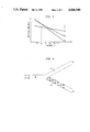
- FIG. 1 shows a cut-away perspective view of a first embodiment of the optical waveguide junction for mode sorting according to the present invention
- FIG. 2 shows a cut-away perspective view of a second embodiment of the optical waveguide junction according to the present invention
- FIG. 3 shows a graph of the dispersion curves for a wavelength multiplexer according to the present invention
- FIG. 4 shows a top plan view of a third embodiment of the optical waveguide junction according to the present invention.
- FIG. 5(a), 5(b), and 5(c) shows a highly simplified representation of the field distribution in the optical waveguide junction and along three output waveguides for three distinct modes of optical radiation according to the present invention.
- FIG. 1 there is shown a cut-away perspective view of an optical waveguide junction for mode sorting of optical radiation according to the present invention. As will be discussed subsequently, a similar configuration may also be used for sorting by wavelength or polarization.
- the device is implemented on substrate 10 on which a layer 11 of optical material has been formed or deposited.
- the layer 11 includes an input multimode waveguide 12 for propagating multimode optical radiation.
- Optical dielectric waveguides have been made by a variety of fabrication methods on substrates such as glass, lithium niobate, and gallium arsenide (GaAs).
- substrates such as glass, lithium niobate, and gallium arsenide (GaAs).
- GaAs gallium arsenide
- most optical communication devices use lithium niobate (or lithium tantalate) or GaAs substrates.
- the refractive index in the guide region must be greater than that of the substrate and the surrounding medium which is generally air.
- a plurality of n spaced apart output waveguides 13, 14, 15 and 16 is disposed on the layer of optical material 11 and coupled at a junction to the input waveguide 12.
- Each of the output waveguides have a different propagation constant (i.e., by having a different width or index of refraction.)
- each of one of the output waveguides 13, 14, 15 and 16 has a width which is different from an adjacent output waveguide.
- the physical layout of the output waveguides is such that each of the output waveguides branch from the junction so that the distance between the edge of the waveguide with the edge of an adjacent waveguide increases from zero, i.e., the output waveguides diverge from the junction.
- the input waveguide is a single multimode waveguide
- each of the output waveguides is a single mode waveguide.
- each of the output waveguides has a width that is monotonically different from an adjacent output waveguide.
- the difference in width between the output waveguides is approximately 1 micron.
- waveguide 13 may have a width of 2 microns, waveguide 14 a width of 3 microns, waveguide 15 a width of 4 microns, and waveguide 16 a width of 5 microns.
- the width of waveguide 12 may be 14 microns.
- each of the waveguides comprise rectilinear strips disposed on said substrate, and at least a portion of the end of the input waveguide is contiguous with each of the output waveguides.
- the output waveguides may have different indices of refraction.
- the multimode input modes will be sorted in a predetermined way into n groups of output modes corresponding to the n output waveguides respectively.
- each of the output waveguides should branch from the junction so that the distance between the edge of the waveguide with the edge of an adjacent waveguide increases from zero.
- each one of the waveguides is composed of a different non-linear optical material, the intensity of the input radiation being sufficient so that the effective index of refraction in each output waveguide is different from the effective index of refraction in an adjacent waveguide.
- the multimode input modes will be sorted in a predetermined way into n groups of output modes corresponding to the n output waveguides respectively.
- Nonlinear optical material is known in the prior art.
- Some silicate glasses are attractive materials for fast all-optical devices because they combine nonlinear index coefficients substantially larger than SiO 2 with low absorption coefficients, high damage threshold, sub-picosecond nonlinear response times, and compatibility with waveguide fabrication processes.
- nonlinear optical materials are multiple quantum well heterostructures consisting, e.g., of ultrathin ( ⁇ 10 Angstrom) alternating layers of the compounds GaAs and Al x Ga 1-x As, at or near 0.85 ⁇ m wavelength.
- a second embodiment of the present invention provides m input waveguides and n output waveguides, where m and n are different integers such as depicted in FIG. 2.
- FIG. 2 depicts a waveguide junction with four input waveguides 17, 18, 19, and 20 (which may be either single mode or multimode), and three output waveguide 21, 22, and 23 (which may also be either single mode or multimode).
- the different input and waveguides may be provided with different widths, indices of refraction, or different materials as in the first embodiment.
- the present invention is also concerned with an optical waveguide junction for sorting by wavelength.
- the wavelength-dependent routing schemes of the junctions according to the present invention are useful for wavelength multiplexing-demultiplexing applications.
- Wavelength multiplexing can be achieved similarly by illuminating the junction from the single-mode channels end.
- These wavelength multiplexers/demultiplexers can be extended to include more wavelength channels by adding single-mode output channels.
- the tapered input channel is used to excite the fundamental mode of the multimode junction.
- the single-mode output channels are designed such that their dispersion curves intersect at different wavelengths, as shown in FIG. 3. As a result, a given input wavelength is routed to the output channel with the highest ⁇ 1 at that particular wavelength.
- FIG. 3 shows a graph of the dispersion curves for three distinct output waveguides as a function of wavelength.
- Dispersion is a parameter which is proportional to the derivative of the index of refraction with respect to the wavelength of light. The difference in the slope of the curves makes it possible to utilize the principle of mode sorting according to the present invention to implement sorting with respect to wavelength.
- the three output waveguides have dispersion curves ⁇ 1 , ⁇ 2 , ⁇ 3 respectively. In the first region of the graph, for wavelengths from 0 to ⁇ a , curve ⁇ 1 has the largest propagation constant.
- a device according to the present invention may be implemented with two output waveguides, the material for each waveguides being selected so that the refractive index is different for different polarizations.
- FIG. 4 we illustrate a top plan view of a third embodiment of the present invention which provides such polarization sorting.
- the input waveguide 40 and one of the output waveguides 43 may be constructed with a polarization insensitive material, such as a multiple quantum well heterostructure of alternating GaAs and Al x Ga 1-x As layers, where x is a positive number less than 1.
- the other output waveguide 44 is constructed with a polarization sensitive material.
- the effect of the present invention is shown when two different polarizations 41 and 42 are provided in the input waveguides 40, and the junction routes one polarization 42 to output waveguide 43 and the other polarization 41 to output waveguide 44.
- the principle of operation of the multichannel waveguide junctions can be demonstrated by an analysis of the physics of propagation of electromagnetic radiation in guided wave optic channels.
- a three-mode GaAs/AlGaAs channel input waveguide e.g., a ridge waveguide
- the three-dimensional refractive-index distribution in this waveguide structure was reduced to the two-dimensional effective-index distribution shown by using the effective-index method.
- the propagation constants of the solitary single-mode channels in the present example are different because of the different channel widths.
- the field distribution of the three local normal modes, at four locations along the junction may be computed, and is shown in FIG.
- the effective index is 3.3700 in the channels and 3.3683 between them; the channel widths of the three waveguides are 5, 7, and 3 ⁇ m, from left to right in the figure, and the wavelength is 1.5 ⁇ m.
- the field distribution of each mode are shown at 0, 2, 8, and 16 ⁇ m channel separation.
- the effective-index n eff distributions at the input and the output are shown in the figure.
- the localization features illustrated by FIG. 5 are characteristic of weakly coupled arrays of waveguides of different uncoupled propagation constants. This is in contrast to the situation in arrays of coupled, identical waveguides, in which the power of each normal mode is spread through the array.
- the first mode i.e., the one with the highest propagation constant
- the next high order mode becomes localized in the channel with the next highest ⁇ 1
- Effective localization takes place when the difference in the ⁇ 1 's of adjacent channels is much larger than the corresponding interchannel coupling coefficient.
- the launched power When one of the guided modes of the multimode waveguide is launched, its power will generally be scattered into the other local modes as it propagates down the branching waveguide. For a sufficiently small branching angle, however, most of the launched power will remain in the original mode. Since the intensity distribution in each local mode becomes localized in a different channel, as is illustrated by FIG. 5, the launched power will then be gradually routed into the appropriate output channel.
- the structures according to the present invention can be readily extended to include more output channels in order to handle a larger number of modes.
- the number of output channels is limited by the increased junction length which is required to achieve effective mode separation with increasing number of modes. This is because a larger number of channels require a smaller difference in the uncoupled channel propagation constants in order to keep the m channels single mode and the multimode waveguide m mode. This small difference, in turn, results in an increase in the channel separation needed for effective localization as well as in smaller branching angles required for small intermode scattering.
- the mode-routing characteristics exhibited by the multichannel waveguide junctions described here may also be useful in performing a variety of guided-wave manipulations. Spatial separation of the modes in multimode channel waveguides is useful in studying the modal properties of such waveguides. Furthermore, by exciting the different modes of the multimode input waveguide (e.g., by using a grating coupler configuration) it should be possible to route the incoming beam to each of the output channels. By illuminating the waveguide junction from the single-mode channels end it is possible to selectively excite the different modes of the multimode waveguide, which can be useful in multichannel signal processing systems based on multimode waveguides. Dynamic variation of the propagation constants of the single-mode channels, e.g., via the electro-optic effect or by employing optical nonlinearities, will make the multichannel junctions useful as multiport optical switches and modulators.
- waveguide junctions might be useful for spatial mode and output wavelength control in semiconductor lasers.
- a semiconductor laser with a waveguide structure as shown in FIG. 1 will oscillate at a desired spatial mode by pumping the multimode waveguide and the channel to which this mode is routed.
Abstract
Description
TiO.sub.2 * Nb.sub.2 O.sub.5 * B.sub.2 O.sub.3 * Na.sub.2 O * SiO.sub.2
Claims (16)
Priority Applications (3)
| Application Number | Priority Date | Filing Date | Title |
|---|---|---|---|
| US07/148,294 US4846540A (en) | 1988-01-25 | 1988-01-25 | Optical wavegide junction |
| CA000587269A CA1290436C (en) | 1988-01-25 | 1988-12-29 | Optical waveguide junction |
| PCT/US1989/000190 WO1989006813A1 (en) | 1988-01-25 | 1989-01-17 | Optical waveguide junction |
Applications Claiming Priority (1)
| Application Number | Priority Date | Filing Date | Title |
|---|---|---|---|
| US07/148,294 US4846540A (en) | 1988-01-25 | 1988-01-25 | Optical wavegide junction |
Publications (1)
| Publication Number | Publication Date |
|---|---|
| US4846540A true US4846540A (en) | 1989-07-11 |
Family
ID=22525133
Family Applications (1)
| Application Number | Title | Priority Date | Filing Date |
|---|---|---|---|
| US07/148,294 Expired - Lifetime US4846540A (en) | 1988-01-25 | 1988-01-25 | Optical wavegide junction |
Country Status (3)
| Country | Link |
|---|---|
| US (1) | US4846540A (en) |
| CA (1) | CA1290436C (en) |
| WO (1) | WO1989006813A1 (en) |
Cited By (43)
| Publication number | Priority date | Publication date | Assignee | Title |
|---|---|---|---|---|
| US4961619A (en) * | 1989-03-02 | 1990-10-09 | At&T Bell Laboratories | Low loss waveguide intersection |
| US5031989A (en) * | 1987-09-16 | 1991-07-16 | Osaka Electric And Communication University | Optical filter coupler |
| US5062681A (en) * | 1990-05-02 | 1991-11-05 | E. I. Du Pont De Nemours And Company | Slot-coupling of optical waveguide to optical waveguide devices |
| US5127081A (en) * | 1990-08-03 | 1992-06-30 | At&T Bell Laboratories | Optical branching waveguide |
| US5134671A (en) * | 1990-08-03 | 1992-07-28 | At&T Bell Laboratories | Monolithic integrated optical amplifier and photodetector |
| DE4206358C1 (en) * | 1992-02-29 | 1993-01-21 | Messerschmitt-Boelkow-Blohm Gmbh, 8012 Ottobrunn, De | Radiation-concentrating system - has planar wave guide arrangements partly coupled to have common light outlet aperture |
| US5289551A (en) * | 1990-11-05 | 1994-02-22 | Nippon Sheet Glass Co., Ltd. | Wye-branching optical circuit |
| US5353273A (en) * | 1992-08-04 | 1994-10-04 | International Business Machines Corporation | Multi-channel optical head and data storage system |
| AU654033B2 (en) * | 1992-08-26 | 1994-10-20 | Alcatel N.V. | Electrically controlled optical switch |
| US5418867A (en) * | 1993-02-02 | 1995-05-23 | Koninklijke Ptt Nederland N.V. | Integrated optical device for manipulating the polarization of optical signals |
| US5461494A (en) | 1986-04-17 | 1995-10-24 | Canon Kabushiki Kaisha | Ferroelectric liquid crystal device having colored film and protective film at non-pixel portions |
| US5463705A (en) * | 1992-11-24 | 1995-10-31 | International Business Machines Corporation | Optical waveguide isolation |
| US5490226A (en) * | 1993-11-16 | 1996-02-06 | Gte Laboratories Incorporated | Zero holding power digital optical switches |
| US5504607A (en) * | 1989-02-08 | 1996-04-02 | British Telecommunications, Plc | Optical interconnection network |
| US5517589A (en) * | 1993-06-23 | 1996-05-14 | Canon Kabushiki Kaisha | Optical wavelength multiplexing and demultiplexing device for multiplexing or demultiplexing light having a plurality of modes and photodetector using the same |
| US5524076A (en) * | 1994-01-28 | 1996-06-04 | Northern Telecom Limited | Chirp control of a Mach-Zehnder optical modulator using non-equal power splitting |
| US5537497A (en) * | 1993-11-16 | 1996-07-16 | Gte Laboratories Incorporated | Optimized electrode geometries for digital optical switches |
| US5574289A (en) * | 1992-02-28 | 1996-11-12 | Hitachi, Ltd. | Semiconductor optical integrated device and light receiver using said device |
| US5627929A (en) * | 1995-05-04 | 1997-05-06 | Sandia Corporation | Integrated optical XY coupler |
| WO1997023969A1 (en) * | 1995-12-22 | 1997-07-03 | Corning Incorporated | Wavelength demultiplexer constructed using integrated optics |
| US5757995A (en) * | 1995-12-27 | 1998-05-26 | Nhk Spring Co., Ltd. | Optical coupler |
| WO1999017140A1 (en) * | 1997-09-26 | 1999-04-08 | Gte Laboratories Incorporated | Tightly curved digital optical switches |
| US6141152A (en) * | 1996-07-01 | 2000-10-31 | Corning Incorporated | Multiplexer/demutiplexer with flattened spectral response |
| US6580844B2 (en) * | 2001-04-24 | 2003-06-17 | Lucent Technologies Inc. | Broadband wavelength-division multiplexer/demultiplexer |
| US20030133663A1 (en) * | 2002-01-16 | 2003-07-17 | Jds Uniphase Corporation | Integrated optical splitter |
| WO2004015470A1 (en) * | 2002-08-08 | 2004-02-19 | Agere Systems Inc. | Optical device |
| US20040151423A1 (en) * | 2001-12-20 | 2004-08-05 | Lynx Photonics Networks Inc. | High-tolerance broadband-optical switch in planar lightwave circuits |
| US20040212876A1 (en) * | 2003-02-28 | 2004-10-28 | Bhowmik Achintya K. | Wavelength-tunable amplified optical splitter |
| WO2004104660A1 (en) * | 2003-05-22 | 2004-12-02 | Lionix B.V. | Device, assembly and methods for wavelength-dependent treatment of optical signals |
| WO2006060875A1 (en) * | 2004-12-09 | 2006-06-15 | Rpo Pty Limited | Optical power distribution devices |
| US20100188367A1 (en) * | 2009-01-23 | 2010-07-29 | Nitto Denko Corporation | Optical waveguide with light emitting device and optical touch panel |
| US20100290626A1 (en) * | 2008-01-28 | 2010-11-18 | Qinetiq Limited | Optical transmitters and receivers for quantum key distribution |
| US20100293380A1 (en) * | 2008-01-25 | 2010-11-18 | Qinetiq Limited | Quantum cryptography apparatus |
| US20100329459A1 (en) * | 2008-01-25 | 2010-12-30 | Qinetiq Limited | Multi-community network with quantum key distribution |
| US20110064222A1 (en) * | 2008-05-19 | 2011-03-17 | Qinetiq Limited | Quantum key distribution involving moveable key device |
| US20110069972A1 (en) * | 2008-05-19 | 2011-03-24 | Qinetiq Limited | Multiplexed quantum key distribution |
| US20110228380A1 (en) * | 2008-12-08 | 2011-09-22 | Qinetiq Limited | Non-linear optical device |
| US20110231665A1 (en) * | 2008-12-05 | 2011-09-22 | Qinetiq Limited | Method of performing authentication between network nodes |
| US20120263410A1 (en) * | 2011-04-15 | 2012-10-18 | Dazeng Feng | Device with multiple light sensors receiving light signals from a waveguide |
| US20140023310A1 (en) * | 2011-02-23 | 2014-01-23 | Sumitomo Osaka Cement Co Ltd | Optical modulator |
| US20160070063A1 (en) * | 2014-09-09 | 2016-03-10 | Hon Hai Precision Industry Co., Ltd. | Optical coupling device, photoelectric conversion device and optical communication device |
| US9692595B2 (en) | 2010-12-02 | 2017-06-27 | Qinetiq Limited | Quantum key distribution |
| US20190086764A1 (en) * | 2016-05-04 | 2019-03-21 | Huawei Technologies Co., Ltd. | Optical switch |
Families Citing this family (8)
| Publication number | Priority date | Publication date | Assignee | Title |
|---|---|---|---|---|
| EP0330457A3 (en) * | 1988-02-26 | 1991-08-07 | Matra Marconi Space UK Limited | Optical in line filters |
| DE69117455T2 (en) * | 1990-12-03 | 1996-09-05 | Nikon Corp | Confocal laser scanning microscope with contrast by difference from interference signals |
| FR2678744A1 (en) * | 1991-07-05 | 1993-01-08 | Alsthom Cge Alcatel | OPTICAL SWITCH WITH ELECTRICAL CONTROL. |
| GB2259580A (en) * | 1991-09-13 | 1993-03-17 | Marconi Gec Ltd | Optical switch |
| CA2136752C (en) * | 1992-06-26 | 2003-04-15 | James Charles Brown, Jr. | Multi-branch digital optical switch |
| US5473714A (en) * | 1994-04-29 | 1995-12-05 | At&T Corp. | Optical fiber system using tapered fiber devices |
| ES2160268T3 (en) * | 1996-01-25 | 2001-11-01 | Infineon Technologies Ag | PROCEDURE FOR THE OPERATION OF A PHASE NETWORK. |
| DE19642904C2 (en) * | 1996-10-17 | 2003-10-30 | Ernst-August Stehr | Device for modulating light |
Citations (7)
| Publication number | Priority date | Publication date | Assignee | Title |
|---|---|---|---|---|
| US4139259A (en) * | 1976-01-12 | 1979-02-13 | Siemens Aktiengesellschaft | Light distributor for optical communication systems |
| US4168107A (en) * | 1978-03-30 | 1979-09-18 | Sperry Rand Corporation | Multimode optic device |
| US4674827A (en) * | 1982-05-20 | 1987-06-23 | Masayuki Izutsu | Slab-type optical device |
| US4722583A (en) * | 1984-12-19 | 1988-02-02 | Plessey Overseas Limited | Modulators |
| US4737002A (en) * | 1984-11-21 | 1988-04-12 | The General Electric Company, P.L.C. | Tunable optical directional couplers |
| US4738502A (en) * | 1983-02-10 | 1988-04-19 | Omron Tateisi Electronics Co. | Optical deflector |
| JPH0637531A (en) * | 1992-07-17 | 1994-02-10 | Sansei Denki Kk | Wide band helical antenna and its production |
-
1988
- 1988-01-25 US US07/148,294 patent/US4846540A/en not_active Expired - Lifetime
- 1988-12-29 CA CA000587269A patent/CA1290436C/en not_active Expired - Lifetime
-
1989
- 1989-01-17 WO PCT/US1989/000190 patent/WO1989006813A1/en unknown
Patent Citations (7)
| Publication number | Priority date | Publication date | Assignee | Title |
|---|---|---|---|---|
| US4139259A (en) * | 1976-01-12 | 1979-02-13 | Siemens Aktiengesellschaft | Light distributor for optical communication systems |
| US4168107A (en) * | 1978-03-30 | 1979-09-18 | Sperry Rand Corporation | Multimode optic device |
| US4674827A (en) * | 1982-05-20 | 1987-06-23 | Masayuki Izutsu | Slab-type optical device |
| US4738502A (en) * | 1983-02-10 | 1988-04-19 | Omron Tateisi Electronics Co. | Optical deflector |
| US4737002A (en) * | 1984-11-21 | 1988-04-12 | The General Electric Company, P.L.C. | Tunable optical directional couplers |
| US4722583A (en) * | 1984-12-19 | 1988-02-02 | Plessey Overseas Limited | Modulators |
| JPH0637531A (en) * | 1992-07-17 | 1994-02-10 | Sansei Denki Kk | Wide band helical antenna and its production |
Non-Patent Citations (6)
| Title |
|---|
| "Dielectric Thin Film Optical Branching Waveguide", Appl. Phys. Lett., H. Yajima, Jun. 15, 1973, vol. 22, No. 12, pp. 647-649. |
| "Optical-Waveguide Hybrid Coupler", Optics Letters, M. Izutsu et al., Nov. 1982, vol. 7, No. 11, pp. 549-551. |
| "Synthesis and Characterization of TiO2 -Nb2 O5 Borosilicate Glasses for Nonlinear Optical Waveguides", Mat. Res. Soc. Sym. Proc., E. M. Vogel et al, 1987, vol. 88, pp. 101-105. |
| Dielectric Thin Film Optical Branching Waveguide , Appl. Phys. Lett. , H. Yajima, Jun. 15, 1973, vol. 22, No. 12, pp. 647 649. * |
| Optical Waveguide Hybrid Coupler , Optics Letters , M. Izutsu et al., Nov. 1982, vol. 7, No. 11, pp. 549 551. * |
| Synthesis and Characterization of TiO 2 Nb 2 O 5 Borosilicate Glasses for Nonlinear Optical Waveguides , Mat. Res. Soc. Sym. Proc. , E. M. Vogel et al, 1987, vol. 88, pp. 101 105. * |
Cited By (62)
| Publication number | Priority date | Publication date | Assignee | Title |
|---|---|---|---|---|
| US5461494A (en) | 1986-04-17 | 1995-10-24 | Canon Kabushiki Kaisha | Ferroelectric liquid crystal device having colored film and protective film at non-pixel portions |
| US5031989A (en) * | 1987-09-16 | 1991-07-16 | Osaka Electric And Communication University | Optical filter coupler |
| US5504607A (en) * | 1989-02-08 | 1996-04-02 | British Telecommunications, Plc | Optical interconnection network |
| US4961619A (en) * | 1989-03-02 | 1990-10-09 | At&T Bell Laboratories | Low loss waveguide intersection |
| US5062681A (en) * | 1990-05-02 | 1991-11-05 | E. I. Du Pont De Nemours And Company | Slot-coupling of optical waveguide to optical waveguide devices |
| US5127081A (en) * | 1990-08-03 | 1992-06-30 | At&T Bell Laboratories | Optical branching waveguide |
| US5134671A (en) * | 1990-08-03 | 1992-07-28 | At&T Bell Laboratories | Monolithic integrated optical amplifier and photodetector |
| US5289551A (en) * | 1990-11-05 | 1994-02-22 | Nippon Sheet Glass Co., Ltd. | Wye-branching optical circuit |
| US5574289A (en) * | 1992-02-28 | 1996-11-12 | Hitachi, Ltd. | Semiconductor optical integrated device and light receiver using said device |
| DE4206358C1 (en) * | 1992-02-29 | 1993-01-21 | Messerschmitt-Boelkow-Blohm Gmbh, 8012 Ottobrunn, De | Radiation-concentrating system - has planar wave guide arrangements partly coupled to have common light outlet aperture |
| US5353273A (en) * | 1992-08-04 | 1994-10-04 | International Business Machines Corporation | Multi-channel optical head and data storage system |
| US5537617A (en) * | 1992-08-04 | 1996-07-16 | International Business Machines Corporation | Multi-channel optical head and data storage system |
| AU654033B2 (en) * | 1992-08-26 | 1994-10-20 | Alcatel N.V. | Electrically controlled optical switch |
| US5463705A (en) * | 1992-11-24 | 1995-10-31 | International Business Machines Corporation | Optical waveguide isolation |
| US5418867A (en) * | 1993-02-02 | 1995-05-23 | Koninklijke Ptt Nederland N.V. | Integrated optical device for manipulating the polarization of optical signals |
| US5517589A (en) * | 1993-06-23 | 1996-05-14 | Canon Kabushiki Kaisha | Optical wavelength multiplexing and demultiplexing device for multiplexing or demultiplexing light having a plurality of modes and photodetector using the same |
| US5490226A (en) * | 1993-11-16 | 1996-02-06 | Gte Laboratories Incorporated | Zero holding power digital optical switches |
| US5537497A (en) * | 1993-11-16 | 1996-07-16 | Gte Laboratories Incorporated | Optimized electrode geometries for digital optical switches |
| US5524076A (en) * | 1994-01-28 | 1996-06-04 | Northern Telecom Limited | Chirp control of a Mach-Zehnder optical modulator using non-equal power splitting |
| US5627929A (en) * | 1995-05-04 | 1997-05-06 | Sandia Corporation | Integrated optical XY coupler |
| AU721743B2 (en) * | 1995-12-22 | 2000-07-13 | Corning Incorporated | Wavelength demultiplexer; constructed using integrated optics |
| WO1997023969A1 (en) * | 1995-12-22 | 1997-07-03 | Corning Incorporated | Wavelength demultiplexer constructed using integrated optics |
| US5757995A (en) * | 1995-12-27 | 1998-05-26 | Nhk Spring Co., Ltd. | Optical coupler |
| US6141152A (en) * | 1996-07-01 | 2000-10-31 | Corning Incorporated | Multiplexer/demutiplexer with flattened spectral response |
| US5991475A (en) * | 1997-09-26 | 1999-11-23 | Gte Laboratories Incorporated | Tightly curved digital optical switches |
| WO1999017140A1 (en) * | 1997-09-26 | 1999-04-08 | Gte Laboratories Incorporated | Tightly curved digital optical switches |
| US6580844B2 (en) * | 2001-04-24 | 2003-06-17 | Lucent Technologies Inc. | Broadband wavelength-division multiplexer/demultiplexer |
| US20040151423A1 (en) * | 2001-12-20 | 2004-08-05 | Lynx Photonics Networks Inc. | High-tolerance broadband-optical switch in planar lightwave circuits |
| US7254299B2 (en) * | 2001-12-20 | 2007-08-07 | Lynx Photonic Networks, Inc. | High-tolerance broadband-optical switch in planar lightwave circuits |
| US20030133663A1 (en) * | 2002-01-16 | 2003-07-17 | Jds Uniphase Corporation | Integrated optical splitter |
| WO2004015470A1 (en) * | 2002-08-08 | 2004-02-19 | Agere Systems Inc. | Optical device |
| US20040212876A1 (en) * | 2003-02-28 | 2004-10-28 | Bhowmik Achintya K. | Wavelength-tunable amplified optical splitter |
| US6980355B2 (en) * | 2003-02-28 | 2005-12-27 | Intel Corporation | Wavelength-tunable amplified optical splitter |
| WO2004104660A1 (en) * | 2003-05-22 | 2004-12-02 | Lionix B.V. | Device, assembly and methods for wavelength-dependent treatment of optical signals |
| NL1025226C2 (en) * | 2003-05-22 | 2004-12-14 | Lionix B V | Device, assembly and methods for wavelength-dependent processing of optical signals. |
| WO2006060875A1 (en) * | 2004-12-09 | 2006-06-15 | Rpo Pty Limited | Optical power distribution devices |
| US20060188198A1 (en) * | 2004-12-09 | 2006-08-24 | Rpo Pty Limited | Optical power distribution devices |
| US7421167B2 (en) | 2004-12-09 | 2008-09-02 | Rpo Pty Limited | Optical power distribution devices |
| US8855316B2 (en) | 2008-01-25 | 2014-10-07 | Qinetiq Limited | Quantum cryptography apparatus |
| US8885828B2 (en) | 2008-01-25 | 2014-11-11 | Qinetiq Limited | Multi-community network with quantum key distribution |
| US20100293380A1 (en) * | 2008-01-25 | 2010-11-18 | Qinetiq Limited | Quantum cryptography apparatus |
| US20100329459A1 (en) * | 2008-01-25 | 2010-12-30 | Qinetiq Limited | Multi-community network with quantum key distribution |
| US20100290626A1 (en) * | 2008-01-28 | 2010-11-18 | Qinetiq Limited | Optical transmitters and receivers for quantum key distribution |
| US9148225B2 (en) | 2008-01-28 | 2015-09-29 | Qinetiq Limited | Optical transmitters and receivers for quantum key distribution |
| US8792791B2 (en) | 2008-05-19 | 2014-07-29 | Qinetiq Limited | Multiplexed quantum key distribution |
| US20110069972A1 (en) * | 2008-05-19 | 2011-03-24 | Qinetiq Limited | Multiplexed quantum key distribution |
| US20110064222A1 (en) * | 2008-05-19 | 2011-03-17 | Qinetiq Limited | Quantum key distribution involving moveable key device |
| US8755525B2 (en) | 2008-05-19 | 2014-06-17 | Qinetiq Limited | Quantum key distribution involving moveable key device |
| US20110231665A1 (en) * | 2008-12-05 | 2011-09-22 | Qinetiq Limited | Method of performing authentication between network nodes |
| US8762728B2 (en) | 2008-12-05 | 2014-06-24 | Qinetiq Limited | Method of performing authentication between network nodes |
| US20110228380A1 (en) * | 2008-12-08 | 2011-09-22 | Qinetiq Limited | Non-linear optical device |
| US8749875B2 (en) * | 2008-12-08 | 2014-06-10 | Qinetiq Limited | Non-linear optical device |
| US8358887B2 (en) * | 2009-01-23 | 2013-01-22 | Nitto Denko Corporation | Optical waveguide with light emitting device and optical touch panel |
| US20100188367A1 (en) * | 2009-01-23 | 2010-07-29 | Nitto Denko Corporation | Optical waveguide with light emitting device and optical touch panel |
| US9692595B2 (en) | 2010-12-02 | 2017-06-27 | Qinetiq Limited | Quantum key distribution |
| US20140023310A1 (en) * | 2011-02-23 | 2014-01-23 | Sumitomo Osaka Cement Co Ltd | Optical modulator |
| US8923673B2 (en) * | 2011-02-23 | 2014-12-30 | Sumitomo Osaka Cement Co., Ltd. | Optical modulator |
| US8989540B2 (en) * | 2011-04-15 | 2015-03-24 | Kotura, Inc. | Device with multiple light sensors receiving light signals from a waveguide |
| US20120263410A1 (en) * | 2011-04-15 | 2012-10-18 | Dazeng Feng | Device with multiple light sensors receiving light signals from a waveguide |
| US20160070063A1 (en) * | 2014-09-09 | 2016-03-10 | Hon Hai Precision Industry Co., Ltd. | Optical coupling device, photoelectric conversion device and optical communication device |
| US20190086764A1 (en) * | 2016-05-04 | 2019-03-21 | Huawei Technologies Co., Ltd. | Optical switch |
| US10481466B2 (en) * | 2016-05-04 | 2019-11-19 | Huawei Technolgies Co., Ltd. | Optical switch |
Also Published As
| Publication number | Publication date |
|---|---|
| CA1290436C (en) | 1991-10-08 |
| WO1989006813A1 (en) | 1989-07-27 |
Similar Documents
| Publication | Publication Date | Title |
|---|---|---|
| US4846540A (en) | Optical wavegide junction | |
| Toney | Lithium niobate photonics | |
| US5937115A (en) | Switchable optical components/structures and methods for the fabrication thereof | |
| US4998793A (en) | Adiabatic polarization manipulating device | |
| US4881791A (en) | Optical device | |
| US5937113A (en) | Optical grating-based device having a slab waveguide polarization compensating region | |
| CA2363630C (en) | Integrated optical switches using nonlinear optical mediums | |
| EP0470249B1 (en) | Electric field induced quantum well waveguides | |
| US7630603B2 (en) | Optical waveguide ring resonator with photo-tunneling input/output port | |
| US20050002605A1 (en) | Light control element and light control device | |
| Chen et al. | Subwavelength grating waveguide devices for telecommunications applications | |
| EP0234127B1 (en) | Optical coupler | |
| JPH05173202A (en) | Light switch | |
| JP2644060B2 (en) | Adiabatic polarization control device | |
| US20060062529A1 (en) | Optical switches | |
| Sumi et al. | Ultra-broadband add-drop filter/switch circuit using subwavelength grating waveguides | |
| EP0821263B1 (en) | Optical non-linear branching element | |
| US6728438B2 (en) | Externally controllable waveguide type higher order mode generator | |
| US3990775A (en) | Thin-film optical waveguide | |
| US6510259B1 (en) | Optical switch using an integrated Mach-Zehnder interferometer having a movable phase shifter and asymmetric arms | |
| Nishihara et al. | Optical integrated circuits | |
| Mao et al. | An ARROW optical wavelength filter: design and analysis | |
| US20050152649A1 (en) | Device for directional and wavelength-selective optical coupling | |
| US6563965B1 (en) | Analog optical switch using an integrated Mach-Zehnder interferometer having a moveable phase shifter | |
| EP0825479A1 (en) | Optical non-linear branching element with MZ interferometer |
Legal Events
| Date | Code | Title | Description |
|---|---|---|---|
| AS | Assignment |
Owner name: BELL COMMUNICATIONS RESEARCH INC., 290 WEST MOUNT Free format text: ASSIGNMENT OF ASSIGNORS INTEREST.;ASSIGNOR:KAPON, ELYAHOU;REEL/FRAME:004876/0851 Effective date: 19880121 Owner name: BELL COMMUNICATIONS RESEARCH INC., A CORP. OF DE, Free format text: ASSIGNMENT OF ASSIGNORS INTEREST;ASSIGNOR:KAPON, ELYAHOU;REEL/FRAME:004876/0851 Effective date: 19880121 |
|
| STCF | Information on status: patent grant |
Free format text: PATENTED CASE |
|
| CC | Certificate of correction | ||
| FPAY | Fee payment |
Year of fee payment: 4 |
|
| FEPP | Fee payment procedure |
Free format text: PAYOR NUMBER ASSIGNED (ORIGINAL EVENT CODE: ASPN); ENTITY STATUS OF PATENT OWNER: LARGE ENTITY |
|
| FPAY | Fee payment |
Year of fee payment: 8 |
|
| AS | Assignment |
Owner name: TELCORDIA TECHNOLOGIES, INC., NEW JERSEY Free format text: CHANGE OF NAME;ASSIGNOR:BELL COMMUNICATIONS RESEARCH, INC.;REEL/FRAME:010263/0311 Effective date: 19990316 |
|
| FPAY | Fee payment |
Year of fee payment: 12 |
|
| AS | Assignment |
Owner name: JPMORGAN CHASE BANK, N.A., AS ADMINISTRATIVE AGENT Free format text: SECURITY AGREEMENT;ASSIGNOR:TELCORDIA TECHNOLOGIES, INC.;REEL/FRAME:015886/0001 Effective date: 20050315 |
|
| AS | Assignment |
Owner name: TELCORDIA TECHNOLOGIES, INC., NEW JERSEY Free format text: TERMINATION AND RELEASE OF SECURITY INTEREST IN PATENT RIGHTS;ASSIGNOR:JPMORGAN CHASE BANK, N.A., AS ADMINISTRATIVE AGENT;REEL/FRAME:019520/0174 Effective date: 20070629 Owner name: TELCORDIA TECHNOLOGIES, INC.,NEW JERSEY Free format text: TERMINATION AND RELEASE OF SECURITY INTEREST IN PATENT RIGHTS;ASSIGNOR:JPMORGAN CHASE BANK, N.A., AS ADMINISTRATIVE AGENT;REEL/FRAME:019520/0174 Effective date: 20070629 |
|
| AS | Assignment |
Owner name: WILMINGTON TRUST COMPANY, AS COLLATERAL AGENT, DEL Free format text: SECURITY AGREEMENT;ASSIGNOR:TELCORDIA TECHNOLOGIES, INC.;REEL/FRAME:019562/0309 Effective date: 20070629 Owner name: WILMINGTON TRUST COMPANY, AS COLLATERAL AGENT,DELA Free format text: SECURITY AGREEMENT;ASSIGNOR:TELCORDIA TECHNOLOGIES, INC.;REEL/FRAME:019562/0309 Effective date: 20070629 |
|
| AS | Assignment |
Owner name: TELCORDIA TECHNOLOGIES, INC.,NEW JERSEY Free format text: RELEASE;ASSIGNOR:WILMINGTON TRUST COMPANY, AS COLLATERAL AGENT;REEL/FRAME:024515/0622 Effective date: 20100430 Owner name: TELCORDIA TECHNOLOGIES, INC., NEW JERSEY Free format text: RELEASE;ASSIGNOR:WILMINGTON TRUST COMPANY, AS COLLATERAL AGENT;REEL/FRAME:024515/0622 Effective date: 20100430 |