US4849366A - Method of making a gated isolated structure - Google Patents
Method of making a gated isolated structure Download PDFInfo
- Publication number
- US4849366A US4849366A US07/144,272 US14427288A US4849366A US 4849366 A US4849366 A US 4849366A US 14427288 A US14427288 A US 14427288A US 4849366 A US4849366 A US 4849366A
- Authority
- US
- United States
- Prior art keywords
- layer
- radiation
- oxide
- gate
- silicon nitride
- Prior art date
- Legal status (The legal status is an assumption and is not a legal conclusion. Google has not performed a legal analysis and makes no representation as to the accuracy of the status listed.)
- Expired - Fee Related
Links
Images


Classifications
-
- H—ELECTRICITY
- H01—ELECTRIC ELEMENTS
- H01L—SEMICONDUCTOR DEVICES NOT COVERED BY CLASS H10
- H01L21/00—Processes or apparatus adapted for the manufacture or treatment of semiconductor or solid state devices or of parts thereof
- H01L21/70—Manufacture or treatment of devices consisting of a plurality of solid state components formed in or on a common substrate or of parts thereof; Manufacture of integrated circuit devices or of parts thereof
- H01L21/71—Manufacture of specific parts of devices defined in group H01L21/70
- H01L21/76—Making of isolation regions between components
- H01L21/765—Making of isolation regions between components by field effect
-
- Y—GENERAL TAGGING OF NEW TECHNOLOGICAL DEVELOPMENTS; GENERAL TAGGING OF CROSS-SECTIONAL TECHNOLOGIES SPANNING OVER SEVERAL SECTIONS OF THE IPC; TECHNICAL SUBJECTS COVERED BY FORMER USPC CROSS-REFERENCE ART COLLECTIONS [XRACs] AND DIGESTS
- Y10—TECHNICAL SUBJECTS COVERED BY FORMER USPC
- Y10S—TECHNICAL SUBJECTS COVERED BY FORMER USPC CROSS-REFERENCE ART COLLECTIONS [XRACs] AND DIGESTS
- Y10S438/00—Semiconductor device manufacturing: process
- Y10S438/953—Making radiation resistant device
Definitions
- the p-type substrate of N-channel MOSFET will be inverted to n-type because of the accumulation of trapped positive charges and interface states found in the gate oxide (or other insulator) so that, even without gate bias, these devices have large subthreshold leakage current. It is also expected that an apparent standby current will appear at non-operational states and that circuit function will fail during normal operation cycles with such circuits.
- MOS devices with thick gate oxide layers have larger degradation level.
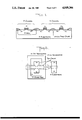
- the electrical isolation between devices is achieved by LOCOS field oxide, as shown in FIG. 1.
- the source/drain regions of neighboring devices and field oxide between them therefore form a parasitic MOSFET, which has a thick equivalent gate oxide.
- the threshold voltage shift induced by irradiation is so substantial that a leakage path underneath the LOCOS region may appear.
- guard rings are added as shown in FIG. 2. This approach, however, is not practical for high packing density because of the waste of chip area. Also, the coupling capacitance to the gate region is too large, which usually reduces the speed of operation. J. E. Schroeder et al., "An Advanced, Radiation Hardened Bulk CMOS/LSI Technology, IEEE Transactions on Nuclear Science, NS-28, No. 6, 4033-4037 (1981).
- FIG. 3 a closed structure is designed as shown in FIG. 3.
- the drain region is surrounded by gate region to cut off the leakage path.
- This construct still has low packing density and large coupling capacitance between the gate and the drain. Again, the speed of operation is reduced.
- This invention relates to a radiation-hardened bulk CMOS isolation structure and a process which eliminates the conventional LOCOS field oxide.
- the structure may be automatically generated by special layout procedures employing computer aided design, CAD. This unique process makes it possible to expeditiously fabricate a radiation-hardened VLSI circuit and to easily modify existing commercial products to form a radiation hardened version without the need for redesigning such product.
- FIG. 1 illustrates a conventional complementary metal oxide semiconductor where the electrical isolation between devices is achieved by a LOCOS field oxide.
- FIG. 2 shows a known CMOS structure having a guard ring surrounding the N-channel transistor.
- FIG. 3 illustrates an inverter and 2-NAND gate employing the closed structure of the prior art where the drain region is surrounded by a gate region.
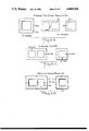
- FIG. 4-1-(a) illustrates a vertical cross-section of a portion of an integrated circuit embodying the invention showing the polysilicon gated isolation structure (GIS) locally adopted as electrical isolation between active N-channel MOSFETs in a CMOS.
- GIS polysilicon gated isolation structure
- FIG. 4-1-(b) represents a top view of the integrated circuit shown in the previous figure, illustrating the GIS, particularly in relation to the N-channels.
- FIGS. 4-2 to 4-6 illustrate the formation of the device of the invention at various stages in the process. The completed device is shown in FIG. 4-6.
- FIGS. 5-0 to 5-7 show the layout procedure employed in developing the GIS.
- FIG. 5-0 shows the pattern generated for the thin oxide regions including the N-channel and P-channel.
- FIG. 5-1 shows the pattern generated for the N-channel thin oxide region.
- FIG. 5-2 shows the modification of the N-channel thin oxide region formed in step 2.
- FIG. 5-3 shows the combining of the P-channel thin oxide region and the modified N-channel thin oxide region.
- Pattern A5 is the actual thin oxide layer used in the photolithography.
- FIG. 5-4 shows the generation of the gated isolation structure for the N-channel device.
- FIG. 5-5 shows the generation of the isolation implant region for the gated isolation structure.
- FIG. 5-6 shows the patterning of the contact regions.
- FIG. 5-7 shows the modification of the contact regions for electrically connecting the gated isolation structure to Vss.
- FIG. 4-1-(a) shows a vertical section of the polysilicon gated isolation structure of the invention.
- the GIS serves to provide local electrical isolation about the active n-MOSFETs in the CMOS integrated circuit figure.
- FIG. 4-1-(b) illustrates a top view of a portion of the CMOS showing the gated isolation structure with respect to the two N-channels, N 1 and N 2 .
- the isolation gate is kept at 0 bias to lower the threshold voltage shift of equivalent GIS MOSFETs after irradiation and to achieve electrical isolation between the active devices.
- a processing wafer typically a p-type substrate with a resistivity of less than 65 ohm-cm and with a (100) orientation, is used.
- An isotropic epitaxial layer is grown on the bare P-substrate to provide latch-up immunity. The thickness of the epitaxial layer depends on the P+ to N- well and N+ to P- substrate rules.
- FIG. 4-3 shows the formation of the N-well 2 and field oxide 3.
- the N-well 2 is selected as the substrate for a P-channel active devices. It is formed in a conventional manner by P 31 ion implantation followed by high temperature drive-in. The implant energy, implant dose and drive-in temperatures are properly adjusted to obtain 3.5 to 4.5 ⁇ m depth for the N-well with a sheet resistance of 1200 to 1500 ohm/sq. to comply with the 2 ⁇ m design rule.
- the field oxide 3 which serves to isolate the P-channel device to P-channel or to N-channel device is grown to 7000 to 8000 Ang. by local oxidation of silicon (LOCOS) processing. The temperature is approximately 980° C. or higher.
- LOCS local oxidation of silicon
- FIG. 4--4 shows the formation of the gated isolation structure.
- a certain amount of B 11 is implanted into the isolation region, shown by the numeral 4, to adjust the threshold voltage of the GIS.
- the dopant concentration is dependent on the threshold voltage shift induced by irradiation and device characteristics, it being understood that junction breakdown may occur at the isolation region/N+ junction if the dopant concentration is too high. Usually the concentration is not higher than lE13 cm-2.
- the composite thermal oxide/nitride/oxynitride (ONO) structure is chosen as the GIS gate insulator 5. These layers are shown in detail on FIGS. 4-4(a) and 4-4-(b).
- the appropriate thickness of these layers depends on the radiation immunity of the composite film, the etching recipe for GIS polysilicon, and the integrity of the gate insulator.
- An insulator composition of 110 Ang. for the thermal bottom oxide, 110 Ang. for the chemical vapor deposition (CVD) intermediate silicon nitride, and 30 to 40 Ang. for the thermal oxynitride layer is typical.
- an ONO structure be chosen as the GIS gate insulator.
- the reason is that the nitride is a better material than thermal oxide with respect to radiation hardness.
- the oxynitride serves as the etching stopper for the GIS polysilicon 6, the thickness thereof being from 3,000 to 4,500 Ang.
- This layer is deposited on the ONO by CVD and doped with POC1 3 to obtain a sheet resistance of 10 to 20 ohm/sq.
- the GIS pattern is defined by using SF 6 /Ar plasma dry etching.
- the etching recipe must be highly selective for the polysilicon to silicon dioxide so that the end point can just stop at the oxynitride layer, consuming at most a small bit of the intermediate nitride. This is illustrated in FIG. 4-4-(a).
- the nitride serves as an oxidation mask for the thin oxide region when the GIS polyoxide 7 is grown.
- the thickness of the GIS polyoxide must not be less than 2,000 Ang.
- a thermal oxide layer may be used for the GIS gate insulator, but this is not preferred because, due to the lack of an oxidation mask, it is not easy to control the thickness and integrity of the GIS polyoxide when the thick residual oxide on top of the thin oxide region is etched back. For this reason, the use of nitride is most desirable.
- FIG. 4-6 shows the formation of the N-channel and P-channel MOSFET.
- the threshold voltage of the N-channel and P-channel MOSFET is adjusted by ion implantation.
- an active gate oxide 8 with a thickness of 250 to 300 Ang. is grown.
- the standard method for preparing the radiation-hardened gate oxide is either to use wet oxygen at 850° C. or dry oxygen with or without HCl at 920°-1000° C.
- subsequent processes are all performed at a temperature lower than that at which the gate oxide is formed. This includes the gate polysilicon 9, 9', and 10, shown in FIG. 4-6.
- the thicknesses of these layers is 4000-5000 Ang.
- the polysilicon gate is defined using SF 6 /Ar plasma etching and an etching recipe similar to that used in forming the gated isolation structure to obtain a reliable gate length.
- the source/drain junctions of N-channel 11 and 11' and P-channel 12 are formed by self-aligned ion implantation into the P-substrate and N-well regions, respectively.
- the dopant is B 11 , for P-channel and P 31 for N-channel, while dopant concentration is on the order of approximately 10 15 .
- the typical access time is approximately 100 nsec. and the maximum stand-by (Icc Sta) and operational (Icc OP) currents are about 50 microamperes and 20 milliamperes, respectively.
- CAD computer-assisted design
- the first step is to search and/or generate by the design rule the pattern for the thin oxide regions including N-channel and P-channel.
- the thin oxide region is represented by A1.
- the search and generation of the N-channel thin oxide region is made by CAD and defined as A2, as shown in FIG. 5-1.
- the searching method takes the intersection of the P-field implantation region and the thin oxide region A1, the P-channel thin oxide region thus equalling A1 minus A2.
- FIG. 5-2-(I) shows the modification of the N-channel thin oxide region from step 2. Initially a design rule check (DRC) is performed. If the spacing between the thin oxide region is equal to or smaller than a1 ⁇ m, the thin oxide regions are directly merged to define the new thin oxide region A3. The merged thin oxide regions are outwardly extended by a2 ⁇ m, as shown in FIG. 5-2-(II), and defined as A4. As illustrated in FIG. 5-3, the P-channel thin oxide regions and the modified N-channel thin oxide regions are united and defined as A5. A5 thus represents the actual thin oxide layer in the photolithography processes.
- DRC design rule check
- FIG. 5-4 shows the generation of the GIS region B for the N-channel device. This region is formed by outwardly extending A4 by a3 ⁇ m and then subtracting the A2 region from the extended A4. (This is done because A2 is included in or extends A4.)
- the generation of the isolation implant region C for the GIS is shown in FIG. 5-5.
- the isolation implant region is directly constructed by outwardly extending the GIS region B by a4 ⁇ m.
- FIG. 5-6 shows the pattern for the contact regions generated by the standard rule to define D1.
- FIG. 5-7 shows the modifications of the contact regions for electrically connecting the GIS to the Vss. This is done by first taking the overlap regions of the Vss metal line and GIS and then inwardly shrinking it by a5 ⁇ m. The GIS is thus electrically connected to ground through the new generated contact. Thereafter, the newly generated contact region is combined with the normally designed contact region and defined as D2.
- Design rule checks (DRC) and electrical rule checks (ERC) are performed.
- the purpose of performing design rule checks is to eliminate the line to line overlap between GIS and active device gate pattern which may result in the formation of a metal ribbon after metal line definition.
- the purpose of performing electrical rule checks is to screen out the electrical floating GIS and contact regions which violate design rule. The abnormal GIS and contact regions are processed further by manual or automatic assignment.
- the GIS of the invention can be adapted as electrical isolation parts not only between N-channels in P-substrates, but also for P-channels in the N-well.
- the conventional LOCOS field oxide will be wholly replaced by GIS.
Abstract
Description
              TABLE 1
______________________________________
BEFORE EXPOSURE    AFTER EXPOSURE
                       Speed               Speed
CHIP  Icc     Icc      (Acc  Icc    Icc    (Acc
No.   (sta)   (OP)     time) (sta)  (OP)   time)
______________________________________
1     .31 uA  1.9 mA   95.4 nS
                             35.0 uA
                                    16.5 mA
                                           85.7 nS
2     .24 uA  1.7 mA   90.0 nS
                             24.0 uA
                                    17.5 mA
                                           89.7 nS
3     .293 uA 4.0 mA   90.3 nS
                             25.0 uA
                                    17.14 mA
                                           77.3 nS
______________________________________
______________________________________ Parameter Dimension, um ______________________________________a1 5a2 2a3 1 a4 0.5 a5 0.5 ______________________________________
Claims (5)
Priority Applications (4)
| Application Number | Priority Date | Filing Date | Title |
|---|---|---|---|
| US07/144,272 US4849366A (en) | 1988-01-15 | 1988-01-15 | Method of making a gated isolated structure |
| EP88309242A EP0324225A3 (en) | 1988-01-15 | 1988-10-04 | Gated isolation structure |
| JP63251729A JPH0783047B2 (en) | 1988-01-15 | 1988-10-05 | Process for forming gate isolation structure |
| US07/300,582 US4937756A (en) | 1988-01-15 | 1989-01-23 | Gated isolated structure |
Applications Claiming Priority (1)
| Application Number | Priority Date | Filing Date | Title |
|---|---|---|---|
| US07/144,272 US4849366A (en) | 1988-01-15 | 1988-01-15 | Method of making a gated isolated structure |
Related Child Applications (1)
| Application Number | Title | Priority Date | Filing Date |
|---|---|---|---|
| US07/300,582 Division US4937756A (en) | 1988-01-15 | 1989-01-23 | Gated isolated structure |
Publications (1)
| Publication Number | Publication Date |
|---|---|
| US4849366A true US4849366A (en) | 1989-07-18 |
Family
ID=22507850
Family Applications (1)
| Application Number | Title | Priority Date | Filing Date |
|---|---|---|---|
| US07/144,272 Expired - Fee Related US4849366A (en) | 1988-01-15 | 1988-01-15 | Method of making a gated isolated structure |
Country Status (3)
| Country | Link |
|---|---|
| US (1) | US4849366A (en) |
| EP (1) | EP0324225A3 (en) |
| JP (1) | JPH0783047B2 (en) |
Cited By (21)
| Publication number | Priority date | Publication date | Assignee | Title |
|---|---|---|---|---|
| US5023190A (en) * | 1990-08-03 | 1991-06-11 | Micron Technology, Inc. | CMOS processes |
| US5187113A (en) * | 1991-05-17 | 1993-02-16 | United Technologies Corporation | Field oxide termination and gate oxide formation |
| US5384278A (en) * | 1992-11-16 | 1995-01-24 | United Technologies Corporation | Tight control of resistor valves in a SRAM process |
| US5393683A (en) * | 1992-05-26 | 1995-02-28 | Micron Technology, Inc. | Method of making semiconductor devices having two-layer gate structure |
| US5536955A (en) * | 1993-03-29 | 1996-07-16 | Toppan Electronics (Usa) Inc. | Electronic devices for use in generating integrated circuit structures and method therefor |
| US5538912A (en) * | 1993-02-01 | 1996-07-23 | Mitsubishi Denki Kabushiki Kaisha | Method of making memory cells with peripheral transistors |
| US5578510A (en) * | 1993-03-30 | 1996-11-26 | Nippon Steel Corporation | Method of making an isolation layer stack semiconductor device |
| US5681770A (en) * | 1995-06-07 | 1997-10-28 | International Business Machines Corporation | Process for making and programming a flash memory array |
| US6033998A (en) * | 1998-03-09 | 2000-03-07 | Lsi Logic Corporation | Method of forming variable thickness gate dielectrics |
| US6083852A (en) * | 1997-05-07 | 2000-07-04 | Applied Materials, Inc. | Method for applying films using reduced deposition rates |
| US6103579A (en) * | 1996-01-31 | 2000-08-15 | Micron Technology, Inc. | Method of isolating a SRAM cell |
| US6127262A (en) * | 1996-06-28 | 2000-10-03 | Applied Materials, Inc. | Method and apparatus for depositing an etch stop layer |
| US6242782B1 (en) * | 1995-10-13 | 2001-06-05 | Micron Technology, Inc. | Circuit for providing isolation of integrated circuit active areas |
| US6511893B1 (en) | 1998-05-05 | 2003-01-28 | Aeroflex Utmc Microelectronics, Inc. | Radiation hardened semiconductor device |
| US6699776B2 (en) * | 1998-12-22 | 2004-03-02 | Kabushiki Kaisha Toshiba | MOSFET gate insulating film and method of manufacturing the same |
| US20040070031A1 (en) * | 2002-10-11 | 2004-04-15 | Shunsuke Baba | Soi mosfet device having second gate electrodes for threshold voltage control |
| US6750107B1 (en) | 1996-01-31 | 2004-06-15 | Micron Technology, Inc. | Method and apparatus for isolating a SRAM cell |
| US20060097293A1 (en) * | 2004-11-08 | 2006-05-11 | Intersil Americas, Inc. | ESD structure |
| US20070018231A1 (en) * | 2005-07-25 | 2007-01-25 | Yuuichiro Mitani | Nonvolatile semiconductor memory device, semiconductor device and manufacturing method of nonvolatile semiconductor memory device |
| US20100038726A1 (en) * | 2008-08-13 | 2010-02-18 | Intersil Americas Inc. | Radiation hardened device |
| CN112687716A (en) * | 2020-12-28 | 2021-04-20 | 中国电子科技集团公司第四十四研究所 | CCD amplifier structure for improving ionization effect irradiation resistance |
Families Citing this family (8)
| Publication number | Priority date | Publication date | Assignee | Title |
|---|---|---|---|---|
| JPH0265254A (en) * | 1988-08-31 | 1990-03-05 | Toshiba Corp | Semiconductor device |
| JPH0817203B2 (en) * | 1989-08-18 | 1996-02-21 | 三菱電機株式会社 | Semiconductor device and manufacturing method thereof |
| JP2598328B2 (en) * | 1989-10-17 | 1997-04-09 | 三菱電機株式会社 | Semiconductor device and manufacturing method thereof |
| JPH0465167A (en) * | 1990-07-05 | 1992-03-02 | Mitsubishi Electric Corp | Semiconductor device |
| US6091630A (en) * | 1999-09-10 | 2000-07-18 | Stmicroelectronics, Inc. | Radiation hardened semiconductor memory |
| EP1094520A1 (en) | 1999-10-22 | 2001-04-25 | STMicroelectronics, Inc. | Radiation hardened semiconductor memory |
| GB2374200A (en) * | 2000-12-21 | 2002-10-09 | Europ Org For Nuclear Research | Radiation tolerant MOS layout |
| KR100665396B1 (en) * | 2004-01-09 | 2007-01-04 | 에스티마이크로일렉트로닉스 엔.브이. | Method of manufacturing a flash memory device |
Citations (5)
| Publication number | Priority date | Publication date | Assignee | Title |
|---|---|---|---|---|
| US3550256A (en) * | 1967-12-21 | 1970-12-29 | Fairchild Camera Instr Co | Control of surface inversion of p- and n-type silicon using dense dielectrics |
| JPS5522878A (en) * | 1978-08-30 | 1980-02-18 | Tdk Corp | Insulation gate type field effect semiconductor device |
| US4561170A (en) * | 1984-07-02 | 1985-12-31 | Texas Instruments Incorporated | Method of making field-plate isolated CMOS devices |
| US4591890A (en) * | 1982-12-20 | 1986-05-27 | Motorola Inc. | Radiation hard MOS devices and methods for the manufacture thereof |
| US4603059A (en) * | 1984-01-23 | 1986-07-29 | Oki Electric Industry Co., Ltd. | Method of manufacturing MIS capacitors for semiconductor IC devices |
Family Cites Families (1)
| Publication number | Priority date | Publication date | Assignee | Title |
|---|---|---|---|---|
| JPS5890758A (en) * | 1981-11-25 | 1983-05-30 | Mitsubishi Electric Corp | Complementary type integrated circuit device |
-
1988
- 1988-01-15 US US07/144,272 patent/US4849366A/en not_active Expired - Fee Related
- 1988-10-04 EP EP88309242A patent/EP0324225A3/en not_active Ceased
- 1988-10-05 JP JP63251729A patent/JPH0783047B2/en not_active Expired - Lifetime
Patent Citations (5)
| Publication number | Priority date | Publication date | Assignee | Title |
|---|---|---|---|---|
| US3550256A (en) * | 1967-12-21 | 1970-12-29 | Fairchild Camera Instr Co | Control of surface inversion of p- and n-type silicon using dense dielectrics |
| JPS5522878A (en) * | 1978-08-30 | 1980-02-18 | Tdk Corp | Insulation gate type field effect semiconductor device |
| US4591890A (en) * | 1982-12-20 | 1986-05-27 | Motorola Inc. | Radiation hard MOS devices and methods for the manufacture thereof |
| US4603059A (en) * | 1984-01-23 | 1986-07-29 | Oki Electric Industry Co., Ltd. | Method of manufacturing MIS capacitors for semiconductor IC devices |
| US4561170A (en) * | 1984-07-02 | 1985-12-31 | Texas Instruments Incorporated | Method of making field-plate isolated CMOS devices |
Non-Patent Citations (12)
| Title |
|---|
| Hoefler, "Varadyne Unveils Details of Field-Shield Process", Electronic News, Jan. 18, 1971, p. 41. |
| Hoefler, Varadyne Unveils Details of Field Shield Process , Electronic News, Jan. 18, 1971, p. 41. * |
| Kump, "Reduced FET Leakage", IBM TDB, vol. 16, No. 5, Oct. 1973, p. 1359. |
| Kump, Reduced FET Leakage , IBM TDB, vol. 16, No. 5, Oct. 1973, p. 1359. * |
| Lin, "Shielded Silicon Gate Complementary MOS Integrated Circuit", IEEE Trans. on Elec. Dev., vol. ED-19, No. 11, Nov. 1972, pp. 1199-1206. |
| Lin, Shielded Silicon Gate Complementary MOS Integrated Circuit , IEEE Trans. on Elec. Dev., vol. ED 19, No. 11, Nov. 1972, pp. 1199 1206. * |
| Moslehi et al., "Thermal Nitridation of Si ANS102 for VLS 1", IEEE Trans. on Elect. Devices, vol. ED-32, No. 2, Feb. 1985, pp. 106-123. |
| Moslehi et al., Thermal Nitridation of Si ANS102 for VLS 1 , IEEE Trans. on Elect. Devices, vol. ED 32, No. 2, Feb. 1985, pp. 106 123. * |
| Sansbury, "MOS Field Threshold Increase by Phosphorous Implanted Field", IEEE Trans. on Elec. Devices, vol. ED-20, No. 5, May 73, pp. 473-476. |
| Sansbury, MOS Field Threshold Increase by Phosphorous Implanted Field , IEEE Trans. on Elec. Devices, vol. ED 20, No. 5, May 73, pp. 473 476. * |
| Terman, "Aluminum-Silicon Self-Aligned Gate Process with Field Shield", IBM TDB, vol. 15, No. 9, Feb. 1973, pp. 2852-2853. |
| Terman, Aluminum Silicon Self Aligned Gate Process with Field Shield , IBM TDB, vol. 15, No. 9, Feb. 1973, pp. 2852 2853. * |
Cited By (39)
| Publication number | Priority date | Publication date | Assignee | Title |
|---|---|---|---|---|
| US5023190A (en) * | 1990-08-03 | 1991-06-11 | Micron Technology, Inc. | CMOS processes |
| US5187113A (en) * | 1991-05-17 | 1993-02-16 | United Technologies Corporation | Field oxide termination and gate oxide formation |
| US5393683A (en) * | 1992-05-26 | 1995-02-28 | Micron Technology, Inc. | Method of making semiconductor devices having two-layer gate structure |
| US5384278A (en) * | 1992-11-16 | 1995-01-24 | United Technologies Corporation | Tight control of resistor valves in a SRAM process |
| US5538912A (en) * | 1993-02-01 | 1996-07-23 | Mitsubishi Denki Kabushiki Kaisha | Method of making memory cells with peripheral transistors |
| US5536955A (en) * | 1993-03-29 | 1996-07-16 | Toppan Electronics (Usa) Inc. | Electronic devices for use in generating integrated circuit structures and method therefor |
| US5578510A (en) * | 1993-03-30 | 1996-11-26 | Nippon Steel Corporation | Method of making an isolation layer stack semiconductor device |
| US5681770A (en) * | 1995-06-07 | 1997-10-28 | International Business Machines Corporation | Process for making and programming a flash memory array |
| US6242782B1 (en) * | 1995-10-13 | 2001-06-05 | Micron Technology, Inc. | Circuit for providing isolation of integrated circuit active areas |
| US6475851B1 (en) * | 1995-10-13 | 2002-11-05 | Micron Technology. Inc. | Circuit for providing isolation of integrated circuit active areas |
| US20040173841A1 (en) * | 1996-01-31 | 2004-09-09 | Static Random Access Memory Cells | Static random access memory cells |
| US6753581B2 (en) | 1996-01-31 | 2004-06-22 | Micron Technology, Inc. | Method of isolating a SRAM cell |
| US6841822B2 (en) | 1996-01-31 | 2005-01-11 | Micron Technology, Inc. | Static random access memory cells |
| US6103579A (en) * | 1996-01-31 | 2000-08-15 | Micron Technology, Inc. | Method of isolating a SRAM cell |
| US6301148B1 (en) | 1996-01-31 | 2001-10-09 | Micron Technology, Inc. | Method of isolating a SRAM cell |
| US6750107B1 (en) | 1996-01-31 | 2004-06-15 | Micron Technology, Inc. | Method and apparatus for isolating a SRAM cell |
| US6383848B1 (en) | 1996-01-31 | 2002-05-07 | Micron Technology, Inc. | Method of isolating a SRAM cell |
| US6127262A (en) * | 1996-06-28 | 2000-10-03 | Applied Materials, Inc. | Method and apparatus for depositing an etch stop layer |
| US6324439B1 (en) | 1997-05-07 | 2001-11-27 | Applied Materials, Inc. | Method and apparatus for applying films using reduced deposition rates |
| US6083852A (en) * | 1997-05-07 | 2000-07-04 | Applied Materials, Inc. | Method for applying films using reduced deposition rates |
| US6033998A (en) * | 1998-03-09 | 2000-03-07 | Lsi Logic Corporation | Method of forming variable thickness gate dielectrics |
| US6511893B1 (en) | 1998-05-05 | 2003-01-28 | Aeroflex Utmc Microelectronics, Inc. | Radiation hardened semiconductor device |
| US6855618B2 (en) | 1998-05-05 | 2005-02-15 | Aeroflex Colorado Springs, Inc. | Radiation hardened semiconductor device |
| US20040166648A1 (en) * | 1998-05-05 | 2004-08-26 | Woodruff Richard L. | Radiation hardened semiconductor device |
| US6699776B2 (en) * | 1998-12-22 | 2004-03-02 | Kabushiki Kaisha Toshiba | MOSFET gate insulating film and method of manufacturing the same |
| US20040070031A1 (en) * | 2002-10-11 | 2004-04-15 | Shunsuke Baba | Soi mosfet device having second gate electrodes for threshold voltage control |
| US6753579B2 (en) * | 2002-10-11 | 2004-06-22 | Oki Electric Industry Co, Ltd. | SOI MOSFET device having second gate electrode for threshold voltage Control |
| US7709907B2 (en) * | 2004-11-08 | 2010-05-04 | Intersil Americas Inc. | ESD structure |
| US20060097293A1 (en) * | 2004-11-08 | 2006-05-11 | Intersil Americas, Inc. | ESD structure |
| US20100171169A1 (en) * | 2005-07-25 | 2010-07-08 | Kabushiki Kaisha Toshiba | Nonvolatile semiconductor memory device, semiconductor device and manufactoring method of nonvolatile semiconductor memory device |
| US20070018231A1 (en) * | 2005-07-25 | 2007-01-25 | Yuuichiro Mitani | Nonvolatile semiconductor memory device, semiconductor device and manufacturing method of nonvolatile semiconductor memory device |
| US7883967B2 (en) | 2005-07-25 | 2011-02-08 | Kabushiki Kaisha Toshiba | Nonvolatile semiconductor memory device, semiconductor device and manufacturing method of nonvolatile semiconductor memory device |
| US8093126B2 (en) | 2005-07-25 | 2012-01-10 | Kabushiki Kaisha Toshiba | Nonvolatile semiconductor memory device, semiconductor device and manufacturing method of nonvolatile semiconductor memory device |
| US20100038726A1 (en) * | 2008-08-13 | 2010-02-18 | Intersil Americas Inc. | Radiation hardened device |
| US7804143B2 (en) | 2008-08-13 | 2010-09-28 | Intersil Americas, Inc. | Radiation hardened device |
| US20100323487A1 (en) * | 2008-08-13 | 2010-12-23 | Intersil Americas Inc. | Radiation hardened device |
| US8268693B2 (en) | 2008-08-13 | 2012-09-18 | Intersil Americas Inc. | Method for fabricating a radiation hardened device |
| CN112687716A (en) * | 2020-12-28 | 2021-04-20 | 中国电子科技集团公司第四十四研究所 | CCD amplifier structure for improving ionization effect irradiation resistance |
| CN112687716B (en) * | 2020-12-28 | 2022-06-24 | 中国电子科技集团公司第四十四研究所 | CCD amplifier structure for improving ionization effect irradiation resistance |
Also Published As
| Publication number | Publication date |
|---|---|
| EP0324225A3 (en) | 1990-03-21 |
| JPH01181459A (en) | 1989-07-19 |
| EP0324225A2 (en) | 1989-07-19 |
| JPH0783047B2 (en) | 1995-09-06 |
Similar Documents
| Publication | Publication Date | Title |
|---|---|---|
| US4849366A (en) | Method of making a gated isolated structure | |
| US4435895A (en) | Process for forming complementary integrated circuit devices | |
| US5420061A (en) | Method for improving latchup immunity in a dual-polysilicon gate process | |
| US5953600A (en) | Fabrication of bipolar/CMOS integrated circuits | |
| US6653709B2 (en) | CMOS output circuit with enhanced ESD protection using drain side implantation | |
| US6297082B1 (en) | Method of fabricating a MOS transistor with local channel ion implantation regions | |
| US4937756A (en) | Gated isolated structure | |
| US20030025165A1 (en) | Buried channel pmos transistor in dual gate cmos with reduced masking steps | |
| JPH06163844A (en) | Manufacture of semiconductor device | |
| JPH05129429A (en) | Semiconductor device and manufacture thereof | |
| US5838033A (en) | Integrated circuit with gate conductor defined resistor | |
| US6218226B1 (en) | Method of forming an ESD protection device | |
| JPH1070266A (en) | Semiconductor device and fabrication thereof | |
| JPH02162761A (en) | Mos-fet and its manufacture | |
| US6528380B2 (en) | Electro static discharge protection n-well ballast resistor device | |
| US6342413B1 (en) | Method of manufacturing semiconductor device | |
| US20010009785A1 (en) | Method of fabricating a supply decoupling capacitor | |
| US5930633A (en) | Integrated butt-contact process in shallow trench isolation | |
| US6303420B1 (en) | Integrated bipolar junction transistor for mixed signal circuits | |
| KR100329895B1 (en) | Semiconductor device with decoupling capacitance and method thereof | |
| US6054354A (en) | High voltage field effect transistors with selective gate depletion | |
| Chen et al. | A high performance submicron CMOS process with self-aligned chan-stop and punch-through implants (twin-tub V) | |
| US20010010954A1 (en) | Method of forming an ESD protection device | |
| JPH08139206A (en) | Semiconductor device and manufacture of the same | |
| KR930005508B1 (en) | Semiconductor device and manufacturing method of the same |
Legal Events
| Date | Code | Title | Description |
|---|---|---|---|
| AS | Assignment |
Owner name: INDUSTRIAL TECHNOLOGY RESEARCH INSTITUTE, NO. 195- Free format text: ASSIGNMENT OF ASSIGNORS INTEREST.;ASSIGNORS:HSU, JE-JUNG;CHEN, HSING-HAI;REEL/FRAME:004866/0165 Effective date: 19880222 Owner name: CHUNG SHAN INSTITUTE OF SCIENCE OF TECHNOLOGY, P.O Free format text: ASSIGNMENT OF ASSIGNORS INTEREST.;ASSIGNORS:HSU, JE-JUNG;CHEN, HSING-HAI;REEL/FRAME:004866/0165 Effective date: 19880222 Owner name: INDUSTRIAL TECHNOLOGY RESEARCH INSTITUTE,TAIWAN Free format text: ASSIGNMENT OF ASSIGNORS INTEREST;ASSIGNORS:HSU, JE-JUNG;CHEN, HSING-HAI;REEL/FRAME:004866/0165 Effective date: 19880222 Owner name: CHUNG SHAN INSTITUTE OF SCIENCE OF TECHNOLOGY,TAIW Free format text: ASSIGNMENT OF ASSIGNORS INTEREST;ASSIGNORS:HSU, JE-JUNG;CHEN, HSING-HAI;REEL/FRAME:004866/0165 Effective date: 19880222 |
|
| CC | Certificate of correction | ||
| FEPP | Fee payment procedure |
Free format text: PAT HLDR NO LONGER CLAIMS SMALL ENT STAT AS NONPROFIT ORG (ORIGINAL EVENT CODE: LSM3); ENTITY STATUS OF PATENT OWNER: LARGE ENTITY Free format text: PAYOR NUMBER ASSIGNED (ORIGINAL EVENT CODE: ASPN); ENTITY STATUS OF PATENT OWNER: LARGE ENTITY |
|
| FPAY | Fee payment |
Year of fee payment: 4 |
|
| FPAY | Fee payment |
Year of fee payment: 8 |
|
| FEPP | Fee payment procedure |
Free format text: PAYOR NUMBER ASSIGNED (ORIGINAL EVENT CODE: ASPN); ENTITY STATUS OF PATENT OWNER: LARGE ENTITY Free format text: PAYER NUMBER DE-ASSIGNED (ORIGINAL EVENT CODE: RMPN); ENTITY STATUS OF PATENT OWNER: LARGE ENTITY |
|
| REMI | Maintenance fee reminder mailed | ||
| LAPS | Lapse for failure to pay maintenance fees | ||
| FP | Lapsed due to failure to pay maintenance fee |
Effective date: 20010718 |
|
| STCH | Information on status: patent discontinuation |
Free format text: PATENT EXPIRED DUE TO NONPAYMENT OF MAINTENANCE FEES UNDER 37 CFR 1.362 |