US4855252A - Process for making self-aligned contacts - Google Patents
Process for making self-aligned contacts Download PDFInfo
- Publication number
- US4855252A US4855252A US07/234,780 US23478088A US4855252A US 4855252 A US4855252 A US 4855252A US 23478088 A US23478088 A US 23478088A US 4855252 A US4855252 A US 4855252A
- Authority
- US
- United States
- Prior art keywords
- layer
- pattern
- polyimide
- depositing
- photoresist
- Prior art date
- Legal status (The legal status is an assumption and is not a legal conclusion. Google has not performed a legal analysis and makes no representation as to the accuracy of the status listed.)
- Expired - Fee Related
Links
Images

Classifications
-
- H—ELECTRICITY
- H01—ELECTRIC ELEMENTS
- H01L—SEMICONDUCTOR DEVICES NOT COVERED BY CLASS H10
- H01L21/00—Processes or apparatus adapted for the manufacture or treatment of semiconductor or solid state devices or of parts thereof
- H01L21/70—Manufacture or treatment of devices consisting of a plurality of solid state components formed in or on a common substrate or of parts thereof; Manufacture of integrated circuit devices or of parts thereof
- H01L21/71—Manufacture of specific parts of devices defined in group H01L21/70
- H01L21/768—Applying interconnections to be used for carrying current between separate components within a device comprising conductors and dielectrics
- H01L21/76838—Applying interconnections to be used for carrying current between separate components within a device comprising conductors and dielectrics characterised by the formation and the after-treatment of the conductors
- H01L21/76885—By forming conductive members before deposition of protective insulating material, e.g. pillars, studs
-
- H—ELECTRICITY
- H01—ELECTRIC ELEMENTS
- H01L—SEMICONDUCTOR DEVICES NOT COVERED BY CLASS H10
- H01L2924/00—Indexing scheme for arrangements or methods for connecting or disconnecting semiconductor or solid-state bodies as covered by H01L24/00
- H01L2924/0001—Technical content checked by a classifier
- H01L2924/0002—Not covered by any one of groups H01L24/00, H01L24/00 and H01L2224/00
Definitions
- This process relates generally to the fabrication of integrated circuits.
- a process for making metal contacts self-aligned to interconnecting metallurgy is described.
- FIG. 1 To better appreciate the problems encountered, as example of a prior art metal line and contact structure is shown in FIG. 1.
- the contacts 10 to the semiconductor devices are first formed, and then in subsequent processing steps, the interconnecting metallurgy 12 is deposited.
- the contacts With the current limitations of conventional optical lithography tools, which have a standard overlay error of approximately 0.45 microns, in order to ensure that one micron wide lines 12 completely overlay the contacts 10, it is necessary that the contacts have a width of approximately 2 microns.
- the ability to increase the maximum wiring density of metal lines 12 would be greatly improved.
- a process for making self-aligned metal lines and contact metallurgy through an insulating/planarizing layer to make contact with semiconductor devices previously formed.
- the essential process steps include:
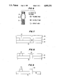
- FIG. 1 is an exploded top view of a semiconductor wafer showing metal lines and contacts as formed in the prior art.
- FIG. 2 shows an exploded top view of a semiconductor wafer showing metal lines and contacts formed according to the invention disclosed herein.
- FIGS. 3-5 show cross-sectional views of a semiconductor wafer at various processing steps according to the method of this invention.
- FIG. 6 shows an exploded top view of a metal line and contact.
- FIGS. 7-9 show cross-sectional views of a semiconductor wafer at various stages of processing.
- substrate 14 is a silicon wafer, but it will be understood by those skilled in the art that substrate 14 could be made of gallium arsenide or other substrates commonly used for making integrated circuits.
- Previously fabricated in substrate 14 are a plurality of semiconductor devices such as FET transistors or bipolar transistors (not shown). The structures and processes used to make these semiconductor devices are not part of the invention herein described.
- BPSG borophosphosilicate glass
- the purpose of the BPSG layer 16 is to insulate the substrate 14 from the metal interconnect lines to be deposited in later processing steps, and also to provide a planar surface upon which the metal is to be deposited.
- a planar surface is important to ensure that the brittle metal lines will not be easily cracked.
- a minimum thickness of 6000 Angstroms is required over the highest point on the substrate 14.
- the insulating/planarizing layer 16 can be comprised of doped or undoped silicon oxide, silicon nitride, phosphosilicate glass, etc.
- the deposition of layer 16 can be by conventional atmospheric pressure chemical vapor deposition (APCVD) or low pressure chemical vapor deposition (LPCVD).
- APCVD atmospheric pressure chemical vapor deposition
- LPCVD low pressure chemical vapor deposition
- a layer of polyimide 18 is formed.
- Liquid polyamic acid is spun on the substrate 14 and then baked at 120° C. for twenty minutes; 200° C. for twenty minutes; and 350° C. for twenty minutes.
- the final thickness of the polyimide should be the approximate thickness of the interconnection metallurgy to be deposited, between 0.5 and 1.5 microns.
- any insulator which has different etch characteristics from layer 16, such as spun on glass or other organic compounds, can be used in place of the polyimide.
- a 2.0 micron thick layer of positive diazonovolak or other positive resist is deposited on top of the polyimide layer 18.
- the thickness of the resist 20 should be approximately twice the thickness of the polyimide layer 18.
- the photoresist layer 20 is then exposed using standard optical or x-ray lithographic tools through a mask (not shown) having the interconnection metallurgy pattern defined.
- the exposed photoresist is then developed in 0.17N KOH or equivalent for other exposure techniques to open up the trenches 22 in photoresist layer 20.
- Photoresist layer 20 is then used as an etch mask and the pattern of trenches 22 is transferred to the polyimide layer 18. This transfer is performed in a reactive ion etch tool using oxygen as the etch gas.
- the etching parameters are as follows:
- the trenches 22 extend throughout both the photoresist layer 20 and the polyimide layer 18.
- the photoresist layer 20 is stripped using a wet chemical solvent, such as N-methylpyrrolidone.
- a second layer of positive diazonovolak photoresist 24 is spun on to a thickness of approximately 1.6-2.0 microns, and then baked for fifteen minutes at 95° C.
- the photoresist layer 24 is then exposed using conventional exposure tools through a mask having a pattern of contacts to substrate 14. Following exposure, the photoresist 24 is then baked at 95° for fifteen minutes.
- the developed photoresist layer 22 is shown in FIG. 5.
- the contact pattern is etched into the polyimide layer 18 and the BPSG layer 16 in a reactive ion etch tool with the following parameters:
- the resulting window 26 can be seen in FIG. 5.
- the photoresist layer 24 is then stripped using a wet chemical solvent.
- the contact window 26 was etched into the BPSG layer using both the photoresist layer 24 and the polyimide layer 18 as etch masks, the contact through the BPSG layer 16 will coincide precisely with the trench 22 which was previously defined to be the area for the metal interconnect lines. The result is a self-aligned contact to metal line structure.
- a layer of metallurgy 28 is conformally deposited using evaporating or sputtering techniques.
- the interconnection metallurgy can be any material conventionally used for such purposes including, but not limited to, aluminum, polysilicon, copper, silicon, titanium, tungsten, silver, gold, or alloys or composites thereof.
- the thickness of the metal over the polyimide layer 18 is preferably 21/2 times the radius of the contact window 26. In this preferred embodiment, the thickness of the metal 28 is 1.5 microns.
- the metal 28 fills the contact window 26 creating a contact stud and also fills the window 22 where the interconnection metallurgy is desired.
- the metal layer 28 is then blanket etched to the surface of polyimide layer 18 in a reactive ion etcher using the following parameters:
- the resulting structure can be seen in FIG. 8.
- the polyimide layer 18 is then removed in an oxygen etch leaving the metal structures 30 and 32 as seen in FIG. 9. Further processing, such as insulator deposition and fabrication of additional layers is then performed.
Abstract
Description
Claims (9)
Priority Applications (3)
| Application Number | Priority Date | Filing Date | Title |
|---|---|---|---|
| US07/234,780 US4855252A (en) | 1988-08-22 | 1988-08-22 | Process for making self-aligned contacts |
| JP1155978A JPH0282626A (en) | 1988-08-22 | 1989-06-20 | Mutual connection method for semiconductor device |
| EP89112163A EP0355339A3 (en) | 1988-08-22 | 1989-07-04 | Process for making self-aligned contacts |
Applications Claiming Priority (1)
| Application Number | Priority Date | Filing Date | Title |
|---|---|---|---|
| US07/234,780 US4855252A (en) | 1988-08-22 | 1988-08-22 | Process for making self-aligned contacts |
Publications (1)
| Publication Number | Publication Date |
|---|---|
| US4855252A true US4855252A (en) | 1989-08-08 |
Family
ID=22882799
Family Applications (1)
| Application Number | Title | Priority Date | Filing Date |
|---|---|---|---|
| US07/234,780 Expired - Fee Related US4855252A (en) | 1988-08-22 | 1988-08-22 | Process for making self-aligned contacts |
Country Status (3)
| Country | Link |
|---|---|
| US (1) | US4855252A (en) |
| EP (1) | EP0355339A3 (en) |
| JP (1) | JPH0282626A (en) |
Cited By (14)
| Publication number | Priority date | Publication date | Assignee | Title |
|---|---|---|---|---|
| US4997789A (en) * | 1988-10-31 | 1991-03-05 | Texas Instruments Incorporated | Aluminum contact etch mask and etchstop for tungsten etchback |
| US5256565A (en) * | 1989-05-08 | 1993-10-26 | The United States Of America As Represented By The United States Department Of Energy | Electrochemical planarization |
| US5868854A (en) * | 1989-02-27 | 1999-02-09 | Hitachi, Ltd. | Method and apparatus for processing samples |
| US6077788A (en) * | 1989-02-27 | 2000-06-20 | Hitachi, Ltd. | Method and apparatus for processing samples |
| US6121129A (en) * | 1997-01-15 | 2000-09-19 | International Business Machines Corporation | Method of contact structure formation |
| US6143655A (en) * | 1998-02-25 | 2000-11-07 | Micron Technology, Inc. | Methods and structures for silver interconnections in integrated circuits |
| US6177342B1 (en) * | 1998-03-17 | 2001-01-23 | United Microelectronics Corp | Method of forming dual damascene interconnects using glue material as plug material |
| US20010003667A1 (en) * | 1998-04-29 | 2001-06-14 | Kie Y. Ahn | Bipolar transistors with low-resistance emitter contacts |
| US6492694B2 (en) | 1998-02-27 | 2002-12-10 | Micron Technology, Inc. | Highly conductive composite polysilicon gate for CMOS integrated circuits |
| US20030209775A1 (en) * | 1998-02-25 | 2003-11-13 | Micron Technology, Inc. | Methods and structures for metal interconnections in integrated circuits |
| US20040219687A1 (en) * | 1989-02-27 | 2004-11-04 | Yoshimi Torii | Method and apparatus for processing samples |
| US20070096322A1 (en) * | 2003-06-10 | 2007-05-03 | Renesas Technology Corp. | Interconnection structure of semiconductor device |
| CN103412423A (en) * | 2013-08-27 | 2013-11-27 | 江西合力泰科技股份有限公司 | Low temperature process for printing titanizing silicon |
| US8816346B2 (en) | 2007-01-04 | 2014-08-26 | Beijing Boe Optoelectronics Technology Co., Ltd. | TFT array substrate and manufacturing method thereof |
Families Citing this family (1)
| Publication number | Priority date | Publication date | Assignee | Title |
|---|---|---|---|---|
| GB2278954A (en) * | 1993-06-07 | 1994-12-14 | Inmos Ltd | Semiconductor device incorporating a contact and manufacture thereof |
Citations (18)
| Publication number | Priority date | Publication date | Assignee | Title |
|---|---|---|---|---|
| US4315984A (en) * | 1979-08-13 | 1982-02-16 | Hitachi, Ltd. | Method of producing a semiconductor device |
| JPS5896752A (en) * | 1981-12-03 | 1983-06-08 | Fujitsu Ltd | Manufacture of semiconductor device |
| US4392298A (en) * | 1981-07-27 | 1983-07-12 | Bell Telephone Laboratories, Incorporated | Integrated circuit device connection process |
| JPS58192350A (en) * | 1982-05-07 | 1983-11-09 | Hitachi Ltd | Semiconductor device |
| JPS5955038A (en) * | 1982-09-22 | 1984-03-29 | Fujitsu Ltd | Formation of multilayer wiring |
| US4512073A (en) * | 1984-02-23 | 1985-04-23 | Rca Corporation | Method of forming self-aligned contact openings |
| US4520041A (en) * | 1982-11-04 | 1985-05-28 | Tokyo Shibaura Denki Kabushiki Kaisha | Method for forming metallization structure having flat surface on semiconductor substrate |
| US4523976A (en) * | 1984-07-02 | 1985-06-18 | Motorola, Inc. | Method for forming semiconductor devices |
| US4544445A (en) * | 1983-03-18 | 1985-10-01 | Commissariat A L'energie Atomique | Process for positioning an interconnection line on an electric contact hole of an integrated circuit |
| JPS60236248A (en) * | 1984-05-09 | 1985-11-25 | Matsushita Electric Ind Co Ltd | Forming layer for multilayer wirings |
| JPS60246649A (en) * | 1984-05-22 | 1985-12-06 | Oki Electric Ind Co Ltd | Manufacture of semiconductor element |
| JPS6194345A (en) * | 1984-10-15 | 1986-05-13 | Sumitomo Electric Ind Ltd | Wiring method of integrated circuit |
| JPS61187346A (en) * | 1985-02-15 | 1986-08-21 | Hitachi Ltd | Semiconductor device |
| US4614021A (en) * | 1985-03-29 | 1986-09-30 | Motorola, Inc. | Pillar via process |
| US4646426A (en) * | 1981-02-16 | 1987-03-03 | Fujitsu Limited | Method of producing MOS FET type semiconductor device |
| US4661204A (en) * | 1985-10-25 | 1987-04-28 | Tandem Computers Inc. | Method for forming vertical interconnects in polyimide insulating layers |
| US4700465A (en) * | 1984-01-27 | 1987-10-20 | Zoran Corporation | Method of selectively making contact structures both with barrier metal and without barrier metal in a single process flow |
| US4797375A (en) * | 1984-10-05 | 1989-01-10 | Honeywell Inc. | Fabrication of metal interconnect for semiconductor device |
Family Cites Families (4)
| Publication number | Priority date | Publication date | Assignee | Title |
|---|---|---|---|---|
| JPS5651827A (en) * | 1979-10-05 | 1981-05-09 | Seiko Epson Corp | Preparation of semiconductor device |
| JPS59202636A (en) * | 1983-05-04 | 1984-11-16 | Hitachi Ltd | Formation of fine pattern |
| US4789648A (en) * | 1985-10-28 | 1988-12-06 | International Business Machines Corporation | Method for producing coplanar multi-level metal/insulator films on a substrate and for forming patterned conductive lines simultaneously with stud vias |
| JPS62128527A (en) * | 1985-11-29 | 1987-06-10 | Matsushita Electric Ind Co Ltd | Manufacture of semiconductor device |
-
1988
- 1988-08-22 US US07/234,780 patent/US4855252A/en not_active Expired - Fee Related
-
1989
- 1989-06-20 JP JP1155978A patent/JPH0282626A/en active Pending
- 1989-07-04 EP EP89112163A patent/EP0355339A3/en not_active Withdrawn
Patent Citations (18)
| Publication number | Priority date | Publication date | Assignee | Title |
|---|---|---|---|---|
| US4315984A (en) * | 1979-08-13 | 1982-02-16 | Hitachi, Ltd. | Method of producing a semiconductor device |
| US4646426A (en) * | 1981-02-16 | 1987-03-03 | Fujitsu Limited | Method of producing MOS FET type semiconductor device |
| US4392298A (en) * | 1981-07-27 | 1983-07-12 | Bell Telephone Laboratories, Incorporated | Integrated circuit device connection process |
| JPS5896752A (en) * | 1981-12-03 | 1983-06-08 | Fujitsu Ltd | Manufacture of semiconductor device |
| JPS58192350A (en) * | 1982-05-07 | 1983-11-09 | Hitachi Ltd | Semiconductor device |
| JPS5955038A (en) * | 1982-09-22 | 1984-03-29 | Fujitsu Ltd | Formation of multilayer wiring |
| US4520041A (en) * | 1982-11-04 | 1985-05-28 | Tokyo Shibaura Denki Kabushiki Kaisha | Method for forming metallization structure having flat surface on semiconductor substrate |
| US4544445A (en) * | 1983-03-18 | 1985-10-01 | Commissariat A L'energie Atomique | Process for positioning an interconnection line on an electric contact hole of an integrated circuit |
| US4700465A (en) * | 1984-01-27 | 1987-10-20 | Zoran Corporation | Method of selectively making contact structures both with barrier metal and without barrier metal in a single process flow |
| US4512073A (en) * | 1984-02-23 | 1985-04-23 | Rca Corporation | Method of forming self-aligned contact openings |
| JPS60236248A (en) * | 1984-05-09 | 1985-11-25 | Matsushita Electric Ind Co Ltd | Forming layer for multilayer wirings |
| JPS60246649A (en) * | 1984-05-22 | 1985-12-06 | Oki Electric Ind Co Ltd | Manufacture of semiconductor element |
| US4523976A (en) * | 1984-07-02 | 1985-06-18 | Motorola, Inc. | Method for forming semiconductor devices |
| US4797375A (en) * | 1984-10-05 | 1989-01-10 | Honeywell Inc. | Fabrication of metal interconnect for semiconductor device |
| JPS6194345A (en) * | 1984-10-15 | 1986-05-13 | Sumitomo Electric Ind Ltd | Wiring method of integrated circuit |
| JPS61187346A (en) * | 1985-02-15 | 1986-08-21 | Hitachi Ltd | Semiconductor device |
| US4614021A (en) * | 1985-03-29 | 1986-09-30 | Motorola, Inc. | Pillar via process |
| US4661204A (en) * | 1985-10-25 | 1987-04-28 | Tandem Computers Inc. | Method for forming vertical interconnects in polyimide insulating layers |
Cited By (32)
| Publication number | Priority date | Publication date | Assignee | Title |
|---|---|---|---|---|
| US4997789A (en) * | 1988-10-31 | 1991-03-05 | Texas Instruments Incorporated | Aluminum contact etch mask and etchstop for tungsten etchback |
| US7132293B2 (en) | 1989-02-27 | 2006-11-07 | Hitachi, Ltd. | Method and apparatus for processing samples |
| US6989228B2 (en) | 1989-02-27 | 2006-01-24 | Hitachi, Ltd | Method and apparatus for processing samples |
| US6656846B2 (en) | 1989-02-27 | 2003-12-02 | Hitachi, Ltd. | Apparatus for processing samples |
| US6077788A (en) * | 1989-02-27 | 2000-06-20 | Hitachi, Ltd. | Method and apparatus for processing samples |
| US5868854A (en) * | 1989-02-27 | 1999-02-09 | Hitachi, Ltd. | Method and apparatus for processing samples |
| US20040219687A1 (en) * | 1989-02-27 | 2004-11-04 | Yoshimi Torii | Method and apparatus for processing samples |
| US5952245A (en) * | 1989-02-27 | 1999-09-14 | Hitachi, Ltd. | Method for processing samples |
| US6537417B2 (en) | 1989-02-27 | 2003-03-25 | Hitachi, Ltd. | Apparatus for processing samples |
| US6537415B2 (en) | 1989-02-27 | 2003-03-25 | Hitachi, Ltd. | Apparatus for processing samples |
| US5256565A (en) * | 1989-05-08 | 1993-10-26 | The United States Of America As Represented By The United States Department Of Energy | Electrochemical planarization |
| US6121129A (en) * | 1997-01-15 | 2000-09-19 | International Business Machines Corporation | Method of contact structure formation |
| US6143655A (en) * | 1998-02-25 | 2000-11-07 | Micron Technology, Inc. | Methods and structures for silver interconnections in integrated circuits |
| US6541859B1 (en) | 1998-02-25 | 2003-04-01 | Micron Technology, Inc. | Methods and structures for silver interconnections in integrated circuits |
| US20030209775A1 (en) * | 1998-02-25 | 2003-11-13 | Micron Technology, Inc. | Methods and structures for metal interconnections in integrated circuits |
| US7186664B2 (en) | 1998-02-25 | 2007-03-06 | Micron Technology, Inc. | Methods and structures for metal interconnections in integrated circuits |
| US20050186773A1 (en) * | 1998-02-25 | 2005-08-25 | Micron Technology, Inc. | Methods and structures for metal interconnections in integrated circuits |
| US6879017B2 (en) | 1998-02-25 | 2005-04-12 | Micron Technology, Inc. | Methods and structures for metal interconnections in integrated circuits |
| US6492694B2 (en) | 1998-02-27 | 2002-12-10 | Micron Technology, Inc. | Highly conductive composite polysilicon gate for CMOS integrated circuits |
| US6573169B2 (en) | 1998-02-27 | 2003-06-03 | Micron Technology, Inc. | Highly conductive composite polysilicon gate for CMOS integrated circuits |
| US6177342B1 (en) * | 1998-03-17 | 2001-01-23 | United Microelectronics Corp | Method of forming dual damascene interconnects using glue material as plug material |
| US7268413B2 (en) | 1998-04-29 | 2007-09-11 | Micron Technology, Inc. | Bipolar transistors with low-resistance emitter contacts |
| US20050026381A1 (en) * | 1998-04-29 | 2005-02-03 | Micron Technology, Inc. | Bipolar transistors with low-resistance emitter contacts |
| US6893933B2 (en) | 1998-04-29 | 2005-05-17 | Micron Technology, Inc. | Bipolar transistors with low-resistance emitter contacts |
| US6815303B2 (en) | 1998-04-29 | 2004-11-09 | Micron Technology, Inc. | Bipolar transistors with low-resistance emitter contacts |
| US20010003667A1 (en) * | 1998-04-29 | 2001-06-14 | Kie Y. Ahn | Bipolar transistors with low-resistance emitter contacts |
| US20050023707A1 (en) * | 1998-04-29 | 2005-02-03 | Micron Technology, Inc. | Bipolar transistors with low-resistance emitter contacts |
| US7489040B2 (en) * | 2003-06-10 | 2009-02-10 | Renesas Technology Corp. | Interconnection structure of semiconductor device |
| US20070096322A1 (en) * | 2003-06-10 | 2007-05-03 | Renesas Technology Corp. | Interconnection structure of semiconductor device |
| US8816346B2 (en) | 2007-01-04 | 2014-08-26 | Beijing Boe Optoelectronics Technology Co., Ltd. | TFT array substrate and manufacturing method thereof |
| CN103412423A (en) * | 2013-08-27 | 2013-11-27 | 江西合力泰科技股份有限公司 | Low temperature process for printing titanizing silicon |
| CN103412423B (en) * | 2013-08-27 | 2016-05-11 | 江西合力泰科技有限公司 | A kind of technique of low temperature printing titanizing silicon |
Also Published As
| Publication number | Publication date |
|---|---|
| EP0355339A3 (en) | 1990-03-21 |
| EP0355339A2 (en) | 1990-02-28 |
| JPH0282626A (en) | 1990-03-23 |
Similar Documents
| Publication | Publication Date | Title |
|---|---|---|
| US4184909A (en) | Method of forming thin film interconnection systems | |
| US4410622A (en) | Forming interconnections for multilevel interconnection metallurgy systems | |
| EP0239756B1 (en) | Process for forming planar chip-level wiring | |
| EP0388862B1 (en) | Fabrication method of a semiconductor device having a planarized surface | |
| US6072237A (en) | Borderless contact structure | |
| US5017510A (en) | Method of making a scalable fuse link element | |
| US4070501A (en) | Forming self-aligned via holes in thin film interconnection systems | |
| US4855252A (en) | Process for making self-aligned contacts | |
| US6165899A (en) | Method for manufacturing semiconductor devices having dual damascene structure | |
| JP2576820B2 (en) | Manufacturing method of contact plug | |
| EP0370935B1 (en) | Method of forming conductive lines and studs | |
| US4933297A (en) | Method for etching windows having different depths | |
| KR100277377B1 (en) | Formation method of contact/through hole | |
| US5384281A (en) | Non-conformal and oxidizable etch stops for submicron features | |
| US6211557B1 (en) | Contact structure using taper contact etching and polycide step | |
| KR20000035246A (en) | Method of fabricating a semiconductor structure | |
| US6737222B2 (en) | Dual damascene process utilizing a bi-layer imaging layer | |
| JP2858837B2 (en) | Method for manufacturing semiconductor device | |
| US5618756A (en) | Selective WSix deposition | |
| JPH09129732A (en) | Semiconductor device manufacturing method | |
| JP3040500B2 (en) | Method for manufacturing semiconductor device | |
| JP2001250861A (en) | Semiconductor device and method of manufacturing the same | |
| JPH08330422A (en) | Semiconductor device and manufacture of the same | |
| JPH0481323B2 (en) | ||
| JPH1174355A (en) | Manufacture of semiconductor device |
Legal Events
| Date | Code | Title | Description |
|---|---|---|---|
| AS | Assignment |
Owner name: INTERNATIONAL BUSINESS MACHINES CORPORATION, A COR Free format text: ASSIGNMENT OF ASSIGNORS INTEREST;ASSIGNORS:PETERMAN, STEVEN;STANASOLOVICH, DAVID;SIGNING DATES FROM 19880811 TO 19880812;REEL/FRAME:004929/0182 Owner name: INTERNATIONAL BUSINESS MACHINES CORPORATION, ARMON Free format text: ASSIGNMENT OF ASSIGNORS INTEREST.;ASSIGNORS:PETERMAN, STEVEN;STANASOLOVICH, DAVID;REEL/FRAME:004929/0182;SIGNING DATES FROM 19880811 TO 19880812 |
|
| FPAY | Fee payment |
Year of fee payment: 4 |
|
| REMI | Maintenance fee reminder mailed | ||
| LAPS | Lapse for failure to pay maintenance fees | ||
| FP | Lapsed due to failure to pay maintenance fee |
Effective date: 19970813 |
|
| STCH | Information on status: patent discontinuation |
Free format text: PATENT EXPIRED DUE TO NONPAYMENT OF MAINTENANCE FEES UNDER 37 CFR 1.362 |