US4855952A - Dram having pip capacitor inside a trench - Google Patents
Dram having pip capacitor inside a trench Download PDFInfo
- Publication number
- US4855952A US4855952A US07/134,867 US13486787A US4855952A US 4855952 A US4855952 A US 4855952A US 13486787 A US13486787 A US 13486787A US 4855952 A US4855952 A US 4855952A
- Authority
- US
- United States
- Prior art keywords
- insulating layer
- trench
- silicon
- memory device
- set forth
- Prior art date
- Legal status (The legal status is an assumption and is not a legal conclusion. Google has not performed a legal analysis and makes no representation as to the accuracy of the status listed.)
- Expired - Lifetime
Links
Images


Classifications
-
- H—ELECTRICITY
- H01—ELECTRIC ELEMENTS
- H01L—SEMICONDUCTOR DEVICES NOT COVERED BY CLASS H10
- H01L21/00—Processes or apparatus adapted for the manufacture or treatment of semiconductor or solid state devices or of parts thereof
- H01L21/70—Manufacture or treatment of devices consisting of a plurality of solid state components formed in or on a common substrate or of parts thereof; Manufacture of integrated circuit devices or of parts thereof
- H01L21/71—Manufacture of specific parts of devices defined in group H01L21/70
- H01L21/76—Making of isolation regions between components
- H01L21/762—Dielectric regions, e.g. EPIC dielectric isolation, LOCOS; Trench refilling techniques, SOI technology, use of channel stoppers
- H01L21/7624—Dielectric regions, e.g. EPIC dielectric isolation, LOCOS; Trench refilling techniques, SOI technology, use of channel stoppers using semiconductor on insulator [SOI] technology
- H01L21/76264—SOI together with lateral isolation, e.g. using local oxidation of silicon, or dielectric or polycristalline material refilled trench or air gap isolation regions, e.g. completely isolated semiconductor islands
-
- H—ELECTRICITY
- H01—ELECTRIC ELEMENTS
- H01L—SEMICONDUCTOR DEVICES NOT COVERED BY CLASS H10
- H01L28/00—Passive two-terminal components without a potential-jump or surface barrier for integrated circuits; Details thereof; Multistep manufacturing processes therefor
- H01L28/40—Capacitors
-
- H—ELECTRICITY
- H10—SEMICONDUCTOR DEVICES; ELECTRIC SOLID-STATE DEVICES NOT OTHERWISE PROVIDED FOR
- H10B—ELECTRONIC MEMORY DEVICES
- H10B12/00—Dynamic random access memory [DRAM] devices
- H10B12/01—Manufacture or treatment
- H10B12/02—Manufacture or treatment for one transistor one-capacitor [1T-1C] memory cells
- H10B12/03—Making the capacitor or connections thereto
- H10B12/038—Making the capacitor or connections thereto the capacitor being in a trench in the substrate
-
- H—ELECTRICITY
- H10—SEMICONDUCTOR DEVICES; ELECTRIC SOLID-STATE DEVICES NOT OTHERWISE PROVIDED FOR
- H10B—ELECTRONIC MEMORY DEVICES
- H10B12/00—Dynamic random access memory [DRAM] devices
- H10B12/30—DRAM devices comprising one-transistor - one-capacitor [1T-1C] memory cells
- H10B12/37—DRAM devices comprising one-transistor - one-capacitor [1T-1C] memory cells the capacitor being at least partially in a trench in the substrate
-
- H—ELECTRICITY
- H01—ELECTRIC ELEMENTS
- H01L—SEMICONDUCTOR DEVICES NOT COVERED BY CLASS H10
- H01L21/00—Processes or apparatus adapted for the manufacture or treatment of semiconductor or solid state devices or of parts thereof
- H01L21/70—Manufacture or treatment of devices consisting of a plurality of solid state components formed in or on a common substrate or of parts thereof; Manufacture of integrated circuit devices or of parts thereof
- H01L21/71—Manufacture of specific parts of devices defined in group H01L21/70
- H01L21/76—Making of isolation regions between components
- H01L21/762—Dielectric regions, e.g. EPIC dielectric isolation, LOCOS; Trench refilling techniques, SOI technology, use of channel stoppers
- H01L21/7624—Dielectric regions, e.g. EPIC dielectric isolation, LOCOS; Trench refilling techniques, SOI technology, use of channel stoppers using semiconductor on insulator [SOI] technology
- H01L21/76264—SOI together with lateral isolation, e.g. using local oxidation of silicon, or dielectric or polycristalline material refilled trench or air gap isolation regions, e.g. completely isolated semiconductor islands
- H01L21/7627—Vertical isolation by full isolation by porous oxide silicon, i.e. FIPOS techniques
-
- H—ELECTRICITY
- H01—ELECTRIC ELEMENTS
- H01L—SEMICONDUCTOR DEVICES NOT COVERED BY CLASS H10
- H01L21/00—Processes or apparatus adapted for the manufacture or treatment of semiconductor or solid state devices or of parts thereof
- H01L21/70—Manufacture or treatment of devices consisting of a plurality of solid state components formed in or on a common substrate or of parts thereof; Manufacture of integrated circuit devices or of parts thereof
- H01L21/71—Manufacture of specific parts of devices defined in group H01L21/70
- H01L21/76—Making of isolation regions between components
- H01L21/762—Dielectric regions, e.g. EPIC dielectric isolation, LOCOS; Trench refilling techniques, SOI technology, use of channel stoppers
- H01L21/7624—Dielectric regions, e.g. EPIC dielectric isolation, LOCOS; Trench refilling techniques, SOI technology, use of channel stoppers using semiconductor on insulator [SOI] technology
- H01L21/76264—SOI together with lateral isolation, e.g. using local oxidation of silicon, or dielectric or polycristalline material refilled trench or air gap isolation regions, e.g. completely isolated semiconductor islands
- H01L21/76286—Lateral isolation by refilling of trenches with polycristalline material
Definitions
- This invention relates to a dynamic random-access memory device, more particularly to an improvement enabling higher levels of integration of memory cells comprising one transistor and one capacitor.
- DRAM Dynamic random-access memory
- an information bit is stored as a capacitor charge in a memory cell usually comprising one capacitor and one transistor.
- An essential requirement for the attainment of extremely high integration densities is to reduce the size of this basic memory cell.
- it is necessary to maintain a certain minimum capacitance generally considered to be 50 fF
- C be the capacitance of the capacitor
- T ox be the thickness of the silicon oxide (SiO 2 ) film
- ⁇ ox be its dielectric constant
- S the capacitance surface area. Then the following relation is approximately true:
- the capacitor area S decreases proportionately and the necessary value of C can only be maintained by reducing the silicon oxide thickness T OX , or increasing ⁇ OX by replacing silicon oxide with a material having a higher dielectric constant.
- Compensating for a reduced S by reducing T OX raises major problems, however.
- the silicon oxide In to maintain the needed C, the silicon oxide must be made so thin that its dielectric breakdown voltage becomes inadequate and the incidence of structural defects rises. There are also problems in using dielectric materials with a higher dielectric constant than silicon oxide.
- Tantalum oxide (Ta 2 O 5 ) has been considered as a candidate material, but a method of forming the necessary Ta 2 O 5 films has not yet been established. Also, a high dielectric constant material is generally associated with a narrow band gap, which offers less resistance to current flow and allows increased leakage current, thereby degrading interface properties as compared with silicon oxide, and causing electrical instability and other problems. For these reasons, it appears difficult to replace silicon oxide with a different material. What is needed is therefore a memory cell structure that combines small cell size with large effective capacitor area.
- the capacitor comprises a dielectric film 4 separating two polysilicon films: one acting as the charge storage electrode 5 1 ; the other acting as the plate electrode 5 2 .
- the capacitor comprising these three films is stacked on top of a gate electrode 8 and a field oxide 2 1 , enabling a larger capacitor area, hence a greater capacitance, to be obtained than in a planar memory cell.
- Another advantage of this structure is that except at the contact 26 between the charge storage electrode 5 1 and the diffusion region 9, the capacitor is separated from the silicon substrate, which reduces the susceptibility of the memory cell to alpha-particle-induced soft errors.
- a disadvantage of this structure as compared with the trench capacitor structure is that it offers less increase in effective capacitor area, permitting only a limited scaling down of memory cell size.
- Another disadvantage of a structure in which the capacitor is stacked on top of the memory cell is that the resulting surface unevenness presents an obstacle to fine patterning.
- the capacitor 13 is created in a trench 3 formed in a silicon substrate 1.
- a dielectric film 4 is grown on the inner surface of the trench 3, then the trench 3 is filled in with polysilicon which forms an electrode 5. Since the capacitor 13 is embedded in a trench 3, compensation for reduction in memory cell size can in principle be obtained by deepening the trench 3 to secure the surface area needed to maintain the required cell capacitance.
- the trench capacitor memory cell structure is thus advantageous for high levels of circuit integration.
- a difficulty with the trench capacitor memory cell is that the trenches of adjacent cells are not completely isolated from one another. If the trenches of adjacent capacitors are too closely spaced, so that their depletion layer approach too closely, leakage current tends to flow between the trenches, degrading such cell characteristics as maximum allowable voltage and charge retention.
- the trenches must therefore be kept a certain distance apart, placing a serious restriction on the scaling down of cell size.
- the trench spacing can be reduced if the silicon substrate is heavily doped with impurities to restrict extending of the depletion layer and block the flow of leakage current, but this method offers only a limited solution, because heavy doping also raises the threshold voltage of the transistors formed on the silicon substrate, so that their junction breakdown voltage becomes intolerably low.
- Another problem with this trench-capacitor memory cell structure is that it is inherently susceptible to alpha-particle-induced soft errors.
- the stacked capacitor memory cell and trench capacitor memory cell of the prior art both offer advantages, but both also suffer from major disadvantages that limit the density of integration of the memory cells.
- a memory cell structure has been considered that combines the advantages of both by forming a PIP (Polysilicon-Insulator-polysilicon) capacitor of the type used in a stacked capacitor memory cell inside a trench.
- This memory cell structure also has disadvantages. The scaling down of its size is limited by the need to form a thick oxide film inside the trench to isolate the lower electrode (the charge storage electrode) from the substrate, which tends to place stress on the trench silicon, and the need to open a contact hole at which the charge storage electrode can make contact with the substrate.
- An object of this invention is to provide a memory cell structure that is free of the disadvantages of the memory cells of the prior art as discussed above and can be used in DRAM devices with ultra-large-scale levels of integration.
- the semiconductor memory device includes a silicon substrate; an insulating layer formed over this substrate and comprised of a first portion and a second portion; at least one monocrystalline silicon island formed within this insulating layer on the first portion thereof, separated from the silicon substrate by the first portion of the insulating layer and laterally spaced from one another by the second portion of the insulating layer, with at least one trench having one wall defined by a side of the at least one monocrystalline silicon islands and extending into the first portion of the insulating layer, and the at least one trench having an opposite wall defined by the second portion of said insulating layer, the second portion of the insulating layer being disposed between monocrystalline silicon islands when there are two or more monocrystalline silicon islands and having an opposite wall defined by the second portion of a lower electrode formed on the inner surface of each of the at least one trench and making contact with the at least one monocrystalline silicon island; a dielectric film formed over the lower electrode; and an upper electrode formed over the dielectric film.
- Information is stored as charge in a capacitor including the lower electrode, the dielectric
- the monocrystalline silicon islands are completely isolated by insulating layer 2 having first and second portions 2a, 2b, respectively. Adjacent trenches are therefore also completely isolated from one another, so no leakage current flows between them. Additionally, when one wall of the trench is formed by the edge of the second portion of the insulating film, the lower electrode inside the trench is surrounded by the insulating film, except where it makes contact with the monocrystalline silicon, hence the structure is protected from alpha particles. Furthermore, parasitic capacitance is reduced, owing to the SOI (Silicon On Insulator) configuration in which the monocrystalline silicon rests on the first insulating layer.
- SOI Silicon On Insulator
- FIG. 1A to FIG. 1I are a series of diagrams illustrating various stages in the fabrication process of a memory device embodying this invention.
- FIG. 2 and FIG. 3 are cross-sectional views of memory devices of the prior art.
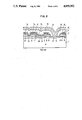
- FIG. 4 is a plan view of the device illustrated in FIG. 1.
- FIG. 1I shows a cross section along line I--I in FIG. 4.
- the structure comprises a silicon substrate 1 1 , a first portion of an insulting layer 2a formed on the silicon substrate 1 1 and consisting of a material such as porous silicon oxide, islands of monocrystalline silicon 1 3 formed on the first portion of an insulating layer 2a, a second portion of an insulating layer 2b that fills in the spaces between the silicon islands 1 3 and joins with the first portion of an insulating layer 2a, and trenches 3 extending through the monocrystalline silicon island 1 3 and into the first portion of an insulating film 2a.
- a material such as porous silicon oxide
- the trench is in the form of a quadrangular prism and is formed at an end of the island 1 3 so that three sides of the prism-shaped trench 3 are coincident or aligned with three edges of the island 1 3 .
- upper parts of the three sides of the prism-shaped trench 3 is defined by the second portion of an insulating layer 2b.
- the trench 3 is defined by the monocrystalline silicon layer 1 3 only at the upper part of the remaining site facing the center of the island 1 3 .
- a lower electrode 5 1 consisting of polysilicon is formed on the inner walls and floor of the trenches 3, a dielectric film 4 is formed over the lower electrode 5 1 , and the remaining space inside the trenches 3 is filled with polysilicon to create an upper electrode 5 2 .
- the lower electrode 5 1 , the dielectric film 4, and the upper electrode 5 2 form an information charge storage capacitor.
- the lower electrode 5 1 is the charge storage electrode; the upper electrode 5 2 is the plate electrode.
- the upper part of the lower electrode 5 1 formed on one side of the trench 3 makes contact with the monocrystalline silicon layer 1 3 .
- An N-type diffusion region 9 is formed in this part of the monocrystalline silicon layer 1 3 , connected to the lower electrode 5 1 by a contact 25.
- This N-type diffusion region 9 is part of an MOS transistor, other parts of the transistor being a second N-type diffusion region 9 and a gate electrode 8 (acting as a word line) located above a gate oxide film 6 situated over the channel between the two N-type diffusion layers 9.
- the second N-type diffusion region 9 is connected via contact window 11 to a bit line 12.
- the bit line 12 is isolated from the word line gate electrode 8 by an inter-layer insulation film 10.
- adjacent trenches 3 are completely isolated from each other by the silicon oxide layer having first and second portions 2a and 2b, so leakage current does not flow between adjacent trenches as it does in the trench capacitor memory cell of the prior art. Excellent cell characteristics can therefore be obtained even if adjacent trenches are closely spaced.
- the lower electrode 5 1 is isolated from the silicon substrate 1 1 and the silicon island 1 3 except at the contact 25 with the N-type diffusion region 9 at the upper part of one side of the trench 3, so the structure is highly resistant to alpha-particle-induced soft errors.
- the contact between the lower electrode 5 1 and the N-type diffusion region 9 on the side wall of the trench 3 is self-aligned and does not require the opening of a contact window by conventional lithography techniques; this factor also contributes to small cell size.
- SOI Silicon On Insulator
- FIG. 1A to FIG. 1I A preferred fabrication process for this memory device is illustrated in FIG. 1A to FIG. 1I.
- the process begins as in FIG. 1A with the deposition of a silicon nitride film 21 on a P-type silicon substrate 1 1 , formation of a resist 22 on the silicon nitride film 21 patterning of the resist 22 by lithography to create an etching mask, and etching of the silicon nitride film 21 to the desired pattern.
- a P + silicon layer 23 is formed by boron ion implantation, after which the resist 22 is removed, hydrogen ions (protons) are implanted through the entire surface at an energy of 50 keV to 100 keV and dose of 5 ⁇ 10 14 cm -2 to 10 ⁇ 10 14 cm -2 , and heat treatment is carried out at 500° C. to 600° C., forming an N-type silicon layer 1 2 below the patterned silicon nitride film 21, as shown in FIG. 1B.
- the structure is then immersed in hydrofluoric acid (HF) with a concentration of about 40% and current is passed through it, using the silicon substrate 1 1 as the anode. This anodization dissolves part of the P-type silicon, creating the porous silicon layer 24 shown in FIG.
- HF hydrofluoric acid
- the next step is heat treatment in an oxidizing atmosphere at 1000° C. to 1100° C.
- the oxidation rate of the porous silicon film 24 is extremely fast, so it is quickly oxidized, leaving islands of N-type silicon layer 1 2 isolated from the silicon substrate 1 1 by thick porous silicon oxide layer having first and second portion 2a and 2b.
- the donors created by proton implantation disappear at heat treatment above 700° C., so the preceding oxidation process converts the N-type silicon layer 1 2 to a P-type silicon layer 1 3 .
- Removal of the silicon nitride film 21 then leaves the structure shown in FIG. 1D. As is seen, the silicon oxide layer 2b isolates the islands 1 3 from each other over their entire depth.
- the bottom of the oxide layer's second portion 2b is continous with the underlying oxide layer's first portion 2a and the top surface of the oxide layer's second portion 2b is coplanar with the top surface of the islands 1 3 .
- the isolation technique just explained is termed FIPOS (Full Isolation by Porous Oxidized Silicon) and has been described by Imai et al. in IEDM Technical Digest 376 (1981).
- the silicon oxide layer 2 formed by the preceding process consists of a first portion of an insulating layer 2 formed on the silicon substrate 1 1 and a second portion of an insulating layer 2b that separates adjacent silicon layer 1 3 .
- trenches 3 are formed to a depth of 3 ⁇ m to 6 ⁇ m by reactive sputter etching, penetrating the silicon layer 1 3 and extending into the first portion of an insulating layer 2a as shown in FIG. 1E.
- the etching mask used during this reactive sputter etching comprises a silicon oxide film patterned by a lithographic technique, and a silicon nitride film.
- the trench 3 is in the form of a quadrangular prism and is formed at an end of the island 1 3 so that three sides of the prism-shaped trench 3 are substantially coincident with three edges at the island 1 3 .
- upper parts of the three sides of the prism-shaped trench 3 is defined by the second portion of an insulating layer 2b.
- the trench 3 is defined by the monocrystalline silicon layer 1 3 only at the upper part of the remaining side facing the center of the island 1 3 .
- the insulating layer's first and second portions 2a and 2b it may be so designed that three walls 25a, 25b and 25c are situated a little outside of the island 1 3 to allow for errors in the alignment during fabrication process.
- the lower electrode 5 1 which forms the charge storage electrode of the capacitor, is created by depositing polysilicon doped with impurities to a thickness of about 2000 ⁇ and patterning it with a lithographic technique, as shown in FIG. 1F.
- a self-aligned contact is formed between one wall of the trench 3 and the silicon layer 1 3 , so there is no need to open a contact window with a separate lithographic process.
- the capacitor insulator 4 is created as shown in FIG. 1G by forming a thin silicon nitride film and/or silicon oxide film with a thickness of about 100 ⁇ to 150 ⁇ .
- the remaining space in the trench 3 is filled in with polysilicon doped with impurities to form an upper electrode 5 2 , the surface of which is smoothed by an etch-back technique. After patterning by lithography, this upper electrode 5 2 forms the plate electrode of the capacitor.
- the capacitor of the memory cell thus comprises a lower electrode 5 1 , a dielectric film 4, and an upper electrode 5 2 formed inside the trench 3.
- a transistor gate oxide film 6 is formed with a thickness of approximately 150 ⁇ to 300 ⁇ .
- a polycide film 8 (a film consisting of polysilicon overlain by a molybdenum or tungsten silicide), which is patterned by a lithographic technique to create a gate electrode 8, which also acts as a word line.
- polycide it is also possible to use silicide, or simply polysilicon.
- the final steps, illustrated in FIG. 1I use standard, well-known techniques to create the N-type diffusion layer 9 that form the transistor source and drain, create inter-layer insulation film 10 of phosphosilicate glass (PSG) or boro-phosphosilicate glass (BPSG), open contact windows 11, and create aluminum or aluminum-alloy metal wiring 12 for the bit lines.
- a standard, well-known technique is also used to create a protective layer, thereby completing the semiconductor device.
Abstract
Description
C=ε.sub.OX S/T.sub.OX
Claims (11)
Applications Claiming Priority (2)
| Application Number | Priority Date | Filing Date | Title |
|---|---|---|---|
| JP61305265A JPS63158869A (en) | 1986-12-23 | 1986-12-23 | Semiconductor memory |
| JP61-305265 | 1986-12-23 |
Publications (1)
| Publication Number | Publication Date |
|---|---|
| US4855952A true US4855952A (en) | 1989-08-08 |
Family
ID=17943020
Family Applications (1)
| Application Number | Title | Priority Date | Filing Date |
|---|---|---|---|
| US07/134,867 Expired - Lifetime US4855952A (en) | 1986-12-23 | 1987-12-18 | Dram having pip capacitor inside a trench |
Country Status (2)
| Country | Link |
|---|---|
| US (1) | US4855952A (en) |
| JP (1) | JPS63158869A (en) |
Cited By (24)
| Publication number | Priority date | Publication date | Assignee | Title |
|---|---|---|---|---|
| US5102819A (en) * | 1988-08-25 | 1992-04-07 | Sony Corporation | Method of making a dram cell |
| US5219779A (en) * | 1989-05-11 | 1993-06-15 | Sharp Kabushiki Kaisha | Memory cell for dynamic random access memory |
| US5258321A (en) * | 1988-01-14 | 1993-11-02 | Mitsubishi Denki Kabushiki Kaisha | Manufacturing method for semiconductor memory device having stacked trench capacitors and improved intercell isolation |
| US5293563A (en) * | 1988-12-29 | 1994-03-08 | Sharp Kabushiki Kaisha | Multi-level memory cell with increased read-out margin |
| US5384474A (en) * | 1992-01-09 | 1995-01-24 | International Business Machines Corporation | Double grid substrate plate trench |
| EP0735595A2 (en) * | 1995-03-27 | 1996-10-02 | Motorola, Inc. | Integrated circuit capacitor having a conductive trench |
| US5594682A (en) * | 1994-06-22 | 1997-01-14 | Industrial Technology Research Institute | High density self-aligned stack in trench DRAM technology |
| US5651860A (en) * | 1996-03-06 | 1997-07-29 | Micron Technology, Inc. | Ion-implanted resist removal method |
| US5654581A (en) * | 1994-12-09 | 1997-08-05 | Lucent Technologies Inc. | Integrated circuit capacitor |
| GB2318681A (en) * | 1996-10-22 | 1998-04-29 | United Microelectronics Corp | Dram cells |
| US5807776A (en) * | 1995-12-06 | 1998-09-15 | Micron Technology, Inc. | Method of forming dynamic random access memory circuitry and dynamic random access memory |
| US6010949A (en) * | 1996-10-21 | 2000-01-04 | Micron Technology, Inc. | Method for removing silicon nitride in the fabrication of semiconductor devices |
| US6040616A (en) * | 1995-06-06 | 2000-03-21 | Lucent Technologies Inc. | Device and method of forming a metal to metal capacitor within an integrated circuit |
| US6150211A (en) * | 1996-12-11 | 2000-11-21 | Micron Technology, Inc. | Methods of forming storage capacitors in integrated circuitry memory cells and integrated circuitry |
| US20030033035A1 (en) * | 2001-08-08 | 2003-02-13 | Mar-Tin Mar | Versatile counting-meter |
| US6583464B1 (en) * | 1997-11-28 | 2003-06-24 | Infineon Technologies Ag | Memory cell using amorphous material to stabilize the boundary face between polycrystalline semiconductor material of a capacitor and monocrystalline semiconductor material of a transistor |
| US6707706B2 (en) * | 2001-06-29 | 2004-03-16 | Kabushiki Kaisha Toshiba | Semiconductor memory device and method for manufacturing the same |
| US20040106299A1 (en) * | 1998-01-23 | 2004-06-03 | Micron Technology, Inc. | Sacrificial self-aligned interconnect structure and method of making |
| US6855976B2 (en) * | 2001-12-27 | 2005-02-15 | Kabushiki Kaisha Toshiba | Semiconductor device using partial SOI substrate and manufacturing method thereof |
| US20050124133A1 (en) * | 2003-12-05 | 2005-06-09 | Kuo-Chi Tu | Method of forming a PIP capacitor |
| US20050275023A1 (en) * | 2000-08-04 | 2005-12-15 | Renesas Technology Corp. | Semiconductor device and method of manufacturing same |
| US20070238244A1 (en) * | 2006-04-11 | 2007-10-11 | Yung-Chang Lin | Trench-capacitor dram device and manufacture method thereof |
| US20220069140A1 (en) * | 2020-08-25 | 2022-03-03 | Lapis Semiconductor Co., Ltd. | Semiconductor device and manufacturing method for semiconductor device |
| US11961921B2 (en) * | 2020-08-25 | 2024-04-16 | Lapis Semiconductor Co., Ltd. | Semiconductor device and manufacturing method for semiconductor device |
Citations (6)
| Publication number | Priority date | Publication date | Assignee | Title |
|---|---|---|---|---|
| US4462048A (en) * | 1982-02-11 | 1984-07-24 | Rca Corporation | Noise reduction circuitry for audio signals |
| US4566025A (en) * | 1982-06-24 | 1986-01-21 | Rca Corporation | CMOS Structure incorporating vertical IGFETS |
| US4577395A (en) * | 1984-01-13 | 1986-03-25 | Kabushiki Kaisha Toshiba | Method of manufacturing semiconductor memory device having trench memory capacitor |
| US4688064A (en) * | 1984-06-05 | 1987-08-18 | Kabushiki Kaisha Toshiba | Dynamic memory cell and method for manufacturing the same |
| US4717942A (en) * | 1983-07-29 | 1988-01-05 | Nec Corporation | Dynamic ram with capacitor groove surrounding switching transistor |
| US4737838A (en) * | 1985-01-30 | 1988-04-12 | Nec Corporation | Capacitor built-in semiconductor integrated circuit and process of fabrication thereof |
Family Cites Families (2)
| Publication number | Priority date | Publication date | Assignee | Title |
|---|---|---|---|---|
| JPS5752150A (en) * | 1980-09-16 | 1982-03-27 | Nippon Telegr & Teleph Corp <Ntt> | Semiconductor device with element forming region surrounded by porous silicon oxide |
| JPS6047458A (en) * | 1983-08-26 | 1985-03-14 | Hitachi Ltd | Soi type mos dynamic memory |
-
1986
- 1986-12-23 JP JP61305265A patent/JPS63158869A/en active Pending
-
1987
- 1987-12-18 US US07/134,867 patent/US4855952A/en not_active Expired - Lifetime
Patent Citations (6)
| Publication number | Priority date | Publication date | Assignee | Title |
|---|---|---|---|---|
| US4462048A (en) * | 1982-02-11 | 1984-07-24 | Rca Corporation | Noise reduction circuitry for audio signals |
| US4566025A (en) * | 1982-06-24 | 1986-01-21 | Rca Corporation | CMOS Structure incorporating vertical IGFETS |
| US4717942A (en) * | 1983-07-29 | 1988-01-05 | Nec Corporation | Dynamic ram with capacitor groove surrounding switching transistor |
| US4577395A (en) * | 1984-01-13 | 1986-03-25 | Kabushiki Kaisha Toshiba | Method of manufacturing semiconductor memory device having trench memory capacitor |
| US4688064A (en) * | 1984-06-05 | 1987-08-18 | Kabushiki Kaisha Toshiba | Dynamic memory cell and method for manufacturing the same |
| US4737838A (en) * | 1985-01-30 | 1988-04-12 | Nec Corporation | Capacitor built-in semiconductor integrated circuit and process of fabrication thereof |
Non-Patent Citations (2)
| Title |
|---|
| "Scaling Consideration and Dielectric Breakdown Improvement of Corrugated Capacitor Cell (ccc) For Future DRAM" Sunami et al. IEDM 84, pp. 232-235 (1984). |
| Scaling Consideration and Dielectric Breakdown Improvement of Corrugated Capacitor Cell (ccc) For Future DRAM Sunami et al. IEDM 84, pp. 232 235 (1984). * |
Cited By (44)
| Publication number | Priority date | Publication date | Assignee | Title |
|---|---|---|---|---|
| US5258321A (en) * | 1988-01-14 | 1993-11-02 | Mitsubishi Denki Kabushiki Kaisha | Manufacturing method for semiconductor memory device having stacked trench capacitors and improved intercell isolation |
| US5102819A (en) * | 1988-08-25 | 1992-04-07 | Sony Corporation | Method of making a dram cell |
| US5293563A (en) * | 1988-12-29 | 1994-03-08 | Sharp Kabushiki Kaisha | Multi-level memory cell with increased read-out margin |
| US5219779A (en) * | 1989-05-11 | 1993-06-15 | Sharp Kabushiki Kaisha | Memory cell for dynamic random access memory |
| US5384474A (en) * | 1992-01-09 | 1995-01-24 | International Business Machines Corporation | Double grid substrate plate trench |
| US5594682A (en) * | 1994-06-22 | 1997-01-14 | Industrial Technology Research Institute | High density self-aligned stack in trench DRAM technology |
| US5654581A (en) * | 1994-12-09 | 1997-08-05 | Lucent Technologies Inc. | Integrated circuit capacitor |
| EP0735595A2 (en) * | 1995-03-27 | 1996-10-02 | Motorola, Inc. | Integrated circuit capacitor having a conductive trench |
| EP0735595A3 (en) * | 1995-03-27 | 1997-01-02 | Motorola Inc | Integrated circuit capacitor having a conductive trench |
| US6040616A (en) * | 1995-06-06 | 2000-03-21 | Lucent Technologies Inc. | Device and method of forming a metal to metal capacitor within an integrated circuit |
| US6437369B1 (en) | 1995-12-06 | 2002-08-20 | Micron Technology, Inc. | Method of forming dynamic random access memory circuitry and dynamic random access memory |
| US5834805A (en) * | 1995-12-06 | 1998-11-10 | Micron Technology, Inc. | Dynamic random access memory circuit array and memory cell |
| US5977578A (en) * | 1995-12-06 | 1999-11-02 | Micron Technology, Inc. | Method of forming dynamic random access memory circuitry and dynamic random access memory |
| US5807776A (en) * | 1995-12-06 | 1998-09-15 | Micron Technology, Inc. | Method of forming dynamic random access memory circuitry and dynamic random access memory |
| US5895272A (en) * | 1996-03-06 | 1999-04-20 | Micron Technology, Inc. | Ion-implanted resist removal method |
| US5651860A (en) * | 1996-03-06 | 1997-07-29 | Micron Technology, Inc. | Ion-implanted resist removal method |
| US6010949A (en) * | 1996-10-21 | 2000-01-04 | Micron Technology, Inc. | Method for removing silicon nitride in the fabrication of semiconductor devices |
| GB2318681B (en) * | 1996-10-22 | 2001-08-29 | United Microelectronics Corp | Silicon on insulator (soi) dram cell structure and process |
| GB2318681A (en) * | 1996-10-22 | 1998-04-29 | United Microelectronics Corp | Dram cells |
| US6399981B2 (en) | 1996-12-11 | 2002-06-04 | Micron Technology, Inc. | Integrated circuitry memory devices |
| US6358812B1 (en) | 1996-12-11 | 2002-03-19 | Micron Technology, Inc. | Methods of forming storage capacitors |
| US6222215B1 (en) * | 1996-12-11 | 2001-04-24 | Micron Technology, Inc. | DRAM circuitry |
| US6150211A (en) * | 1996-12-11 | 2000-11-21 | Micron Technology, Inc. | Methods of forming storage capacitors in integrated circuitry memory cells and integrated circuitry |
| US6583464B1 (en) * | 1997-11-28 | 2003-06-24 | Infineon Technologies Ag | Memory cell using amorphous material to stabilize the boundary face between polycrystalline semiconductor material of a capacitor and monocrystalline semiconductor material of a transistor |
| US20080315330A1 (en) * | 1998-01-23 | 2008-12-25 | Micron Technology, Inc. | Sacrificial self-aligned interconnect structures |
| US20040106299A1 (en) * | 1998-01-23 | 2004-06-03 | Micron Technology, Inc. | Sacrificial self-aligned interconnect structure and method of making |
| US7825450B2 (en) | 1998-01-23 | 2010-11-02 | Micron Technology, Inc. | Sacrificial self-aligned interconnect structures |
| US20060113576A1 (en) * | 1998-01-23 | 2006-06-01 | Walker Michael A | Sacrificial self-aligned interconnect structure |
| US6995072B2 (en) | 1998-01-23 | 2006-02-07 | Micron Technology, Inc. | Method of making sacrificial self-aligned interconnection structure |
| US7427793B2 (en) | 1998-01-23 | 2008-09-23 | Micron Technology, Inc. | Sacrificial self-aligned interconnect structure |
| US20050275023A1 (en) * | 2000-08-04 | 2005-12-15 | Renesas Technology Corp. | Semiconductor device and method of manufacturing same |
| US6707706B2 (en) * | 2001-06-29 | 2004-03-16 | Kabushiki Kaisha Toshiba | Semiconductor memory device and method for manufacturing the same |
| US20030033035A1 (en) * | 2001-08-08 | 2003-02-13 | Mar-Tin Mar | Versatile counting-meter |
| US6855976B2 (en) * | 2001-12-27 | 2005-02-15 | Kabushiki Kaisha Toshiba | Semiconductor device using partial SOI substrate and manufacturing method thereof |
| US7112822B2 (en) | 2001-12-27 | 2006-09-26 | Kabushiki Kaisha Toshiba | Semiconductor device using partial SOI substrate and manufacturing method thereof |
| US20060273330A1 (en) * | 2001-12-27 | 2006-12-07 | Hajime Nagano | Semiconductor device using partial SOI substrate and manufacturing method thereof |
| US7439112B2 (en) | 2001-12-27 | 2008-10-21 | Kabushiki Kaisha Toshiba | Semiconductor device using partial SOI substrate and manufacturing method thereof |
| US20050093066A1 (en) * | 2001-12-27 | 2005-05-05 | Hajime Nagano | Semiconductor device using partial SOI substrate and manufacturing method thereof |
| US7029968B2 (en) | 2003-12-05 | 2006-04-18 | Taiwan Semiconductor Manufacturing Company, Ltd. | Method of forming a PIP capacitor |
| US20050124133A1 (en) * | 2003-12-05 | 2005-06-09 | Kuo-Chi Tu | Method of forming a PIP capacitor |
| US20070238244A1 (en) * | 2006-04-11 | 2007-10-11 | Yung-Chang Lin | Trench-capacitor dram device and manufacture method thereof |
| US7332392B2 (en) | 2006-04-11 | 2008-02-19 | United Microelectronics Corp. | Trench-capacitor DRAM device and manufacture method thereof |
| US20220069140A1 (en) * | 2020-08-25 | 2022-03-03 | Lapis Semiconductor Co., Ltd. | Semiconductor device and manufacturing method for semiconductor device |
| US11961921B2 (en) * | 2020-08-25 | 2024-04-16 | Lapis Semiconductor Co., Ltd. | Semiconductor device and manufacturing method for semiconductor device |
Also Published As
| Publication number | Publication date |
|---|---|
| JPS63158869A (en) | 1988-07-01 |
Similar Documents
| Publication | Publication Date | Title |
|---|---|---|
| US4855952A (en) | Dram having pip capacitor inside a trench | |
| US4922313A (en) | Process for manufacturing semiconductor memory device and product formed thereby | |
| US5504357A (en) | Dynamic random access memory having a vertical transistor | |
| US4353086A (en) | Silicon integrated circuits | |
| EP0430404B1 (en) | Method of manufacturing a capacitor for a DRAM cell | |
| KR100320332B1 (en) | Semiconductor device and manufacturing method thereof | |
| US5162890A (en) | Stacked capacitor with sidewall insulation | |
| US5373170A (en) | Semiconductor memory device having a compact symmetrical layout | |
| EP0167764A2 (en) | Dynamic ram cell | |
| JP2602219B2 (en) | Semiconductor storage device | |
| JPS62286270A (en) | Semiconductor memory | |
| US5299155A (en) | Dynamic random access memory device with capacitor between vertically aligned FETs | |
| US5156993A (en) | Fabricating a memory cell with an improved capacitor | |
| US5326714A (en) | Method of making a fully used tub DRAM cell | |
| US4921816A (en) | Method of making a trench dram | |
| US4921815A (en) | Method of producing a semiconductor memory device having trench capacitors | |
| US5216267A (en) | Stacked capacitor dynamic random access memory with a sloped lower electrode | |
| US6333533B1 (en) | Trench storage DRAM cell with vertical three-sided transfer device | |
| KR920010695B1 (en) | D-ram cell and its manufacturing method | |
| US5396456A (en) | Fully used tub DRAM cell | |
| US4835589A (en) | Ram cell having trench sidewall load | |
| US5183772A (en) | Manufacturing method for a DRAM cell | |
| US5429976A (en) | Self-aligned method for forming polysilicon word lines on top of gate electrodes to increase capacitance of a stacked capacitor in a DRAM cell | |
| JPS63281457A (en) | Semiconductor memory | |
| US5534457A (en) | Method of forming a stacked capacitor with an "I" shaped storage node |
Legal Events
| Date | Code | Title | Description |
|---|---|---|---|
| AS | Assignment |
Owner name: OKI ELECTRIC INDUSTRY CO., LTD., 7-12, TORANOMON 1 Free format text: ASSIGNMENT OF ASSIGNORS INTEREST.;ASSIGNOR:KIYOSUMI, FUMIO;REEL/FRAME:004806/0207 Effective date: 19871021 Owner name: OKI ELECTRIC INDUSTRY CO., LTD., 7-12, TORANOMON 1 Free format text: ASSIGNMENT OF ASSIGNORS INTEREST;ASSIGNOR:KIYOSUMI, FUMIO;REEL/FRAME:004806/0207 Effective date: 19871021 |
|
| STCF | Information on status: patent grant |
Free format text: PATENTED CASE |
|
| FEPP | Fee payment procedure |
Free format text: PAYOR NUMBER ASSIGNED (ORIGINAL EVENT CODE: ASPN); ENTITY STATUS OF PATENT OWNER: LARGE ENTITY |
|
| FPAY | Fee payment |
Year of fee payment: 4 |
|
| FEPP | Fee payment procedure |
Free format text: PAYER NUMBER DE-ASSIGNED (ORIGINAL EVENT CODE: RMPN); ENTITY STATUS OF PATENT OWNER: LARGE ENTITY Free format text: PAYOR NUMBER ASSIGNED (ORIGINAL EVENT CODE: ASPN); ENTITY STATUS OF PATENT OWNER: LARGE ENTITY |
|
| FPAY | Fee payment |
Year of fee payment: 8 |
|
| FPAY | Fee payment |
Year of fee payment: 12 |