US4860262A - Cache memory reset responsive to change in main memory - Google Patents

Cache memory reset responsive to change in main memory Download PDF

Info

Publication number
US4860262A
US4860262A US07/081,925 US8192587A US4860262A US 4860262 A US4860262 A US 4860262A US 8192587 A US8192587 A US 8192587A US 4860262 A US4860262 A US 4860262A
Authority
US
United States
Prior art keywords
bit
word
parity
circuit
nand gate
Prior art date
Legal status (The legal status is an assumption and is not a legal conclusion. Google has not performed a legal analysis and makes no representation as to the accuracy of the status listed.)
Expired - Lifetime
Application number
US07/081,925
Inventor
Edison H. Chiu
Current Assignee (The listed assignees may be inaccurate. Google has not performed a legal analysis and makes no representation or warranty as to the accuracy of the list.)
Texas Instruments Inc
Original Assignee
Texas Instruments Inc
Priority date (The priority date is an assumption and is not a legal conclusion. Google has not performed a legal analysis and makes no representation as to the accuracy of the date listed.)
Filing date
Publication date
Application filed by Texas Instruments Inc filed Critical Texas Instruments Inc
Priority to US07/081,925 priority Critical patent/US4860262A/en
Assigned to TEXAS INSTRUMENTS INCORPORATED reassignment TEXAS INSTRUMENTS INCORPORATED ASSIGNMENT OF ASSIGNORS INTEREST. Assignors: CHIU, EDISON H.
Priority to JP63193577A priority patent/JP3093761B2/en
Application granted granted Critical
Publication of US4860262A publication Critical patent/US4860262A/en
Anticipated expiration legal-status Critical
Expired - Lifetime legal-status Critical Current

Links

Images

Classifications

    • GPHYSICS
    • G06COMPUTING; CALCULATING OR COUNTING
    • G06FELECTRIC DIGITAL DATA PROCESSING
    • G06F11/00Error detection; Error correction; Monitoring
    • G06F11/07Responding to the occurrence of a fault, e.g. fault tolerance
    • G06F11/08Error detection or correction by redundancy in data representation, e.g. by using checking codes
    • G06F11/10Adding special bits or symbols to the coded information, e.g. parity check, casting out 9's or 11's
    • G06F11/1008Adding special bits or symbols to the coded information, e.g. parity check, casting out 9's or 11's in individual solid state devices
    • G06F11/1064Adding special bits or symbols to the coded information, e.g. parity check, casting out 9's or 11's in individual solid state devices in cache or content addressable memories
    • GPHYSICS
    • G11INFORMATION STORAGE
    • G11CSTATIC STORES
    • G11C7/00Arrangements for writing information into, or reading information out from, a digital store
    • G11C7/20Memory cell initialisation circuits, e.g. when powering up or down, memory clear, latent image memory

Definitions

  • This invention relates to word resetting in memories and more particularly to invalidating addresses in cache memories that correspond to the address of a newly written word in the main memory of a digital computer.
  • SRAM static random access memories
  • Another system writes a word of zeros into the pertinent addresses in the auxiliary memories.
  • the disadvantage of this system is that the address register for performing this function is tied up and also the writing mode wastes time.
  • This invention achieves single word reset without significant increase in circuitry.
  • a circuit for a digital memory word reset invalidates a word in a memory by setting all of the bits in that word to zero.
  • a single "valid" bit could obviously be set to zero, but the parity system would then be adversely affected.
  • the parity bit is also set to zero and entered with the reset multi-bit word.
  • the inventive circuit includes a parity generator which is connected to receive a multi-bit input data word and to generate at least one parity bit therefrom. Also included is an internal data bus for storing a multi-bit word to be written into the memory until a write command is issued from the computer system.
  • Reset circuitry includes input gates for receiving the multi-bit input data word.
  • the input gates also are connected to be gated by a word reset signal.
  • a write command is issued and no word reset signal is generated, the multi-bit input data word is transmitted to the internal bus.
  • the parity generator generates a parity bit for the multi-bit word and transmits it to the internal bus.
  • a write command is entered into the internal bus and causes the writing of the contents of the internal bus into the digital memory.
  • any generated parity bit and the multi-bit input data word are blocked from entry to the internal bus. Instead, the input gates, gated by the word reset signal, force the outputs of those gates to zeros, which are then entered in the internal bus.
  • the write signal is delayed to permit this entry of the input gates into the internal bus, then causing the transfer out of the internal bus into the digital memory.
  • the zeros transferred into the data bits represent a partial address.
  • the invention is particularly useful in digital computer systems that involve the use of cache memories.
  • the cache memories may each have a word of data at an address related to an address in the main memory which has exactly the same data.
  • the cache memory having the old data at the related address must have that address invalidated or the contents at that address updated.
  • the invalidation is done by inserting zeros into a portion of the corresponding addresses.
  • a principal object of this invention is to provide a system for resetting a particular address in a memory by gating zeros into that address.
  • Another object of this invention is to provide a system for invalidating memory locations in cache memories whenever a data word at the same memory location in the main memory of a computer system is updated.
  • Another object of this invention is to provide a word invalidation system that provides for invalidation of a word at a given address by immediate entry of zeros and a parallel entry of a corresponding parity bit.
  • the FIGURE is a schematic diagram of the circuitry for resetting a multi-bit word in a digital memory.
  • This invention is directed to circuitry for invalidating addresses in a memory. It is particularly suited for a digital computer system that uses at least one main memory and at least one associated cache memory. When a processor writes into an address in the main memory, if there is a corresponding address in the cache memory, that cache memory must be earmarked as invalid or the contents must be immediately changed to reflect the data written into the main memory. The practical solution is to invalidate the corresponding cache memory location. This invention makes that function economical in time and circuitry.
  • the FIGURE is a schematic diagram of the circuitry in this preferred embodiment that performs the function of invalidating (resetting) a memory location.
  • a portion of an address is actually reset, rather than data at a given address.
  • the input multi-bit data word is represented as signals D0-D8 which are applied to inverters 20-28.
  • the outputs from inverters 20-22 are input to exclusive-OR circuit 12; the output from inverters 23-25 are input to exclusive-OR circuit 14; the outputs from inverters 26-28 are input to exclusive-OR circuit 16.
  • the outputs from exclusive-OR circuits 12, 14 and 16 are input to exclusive-NOR circuit 18 to provide a parity signal.
  • an odd parity system is used which is one wherein an odd number of "1's" in the input multi-bit data word will result in a "1" parity bit. This is of course an engineering design choice.
  • inverters 20-28 respectively are input to NOR gates 30-38, respectively.
  • a word RESET-signal from a computer system is applied to inverter 102 whose output is applied to the input of each of NOR gates 30-38, respectively.
  • inverter 102 The output from inverter 102 is also applied to inverter 90 whose output serves as an input to NAND gate 92.
  • the other input to NAND gate 92 comes from exclusive-NOR gate 18.
  • the word reset signal therefore controls gates 30-38 and 92.
  • the inputs to inverters 40-48 are connected to the outputs or NOR gates 30-38, respectively.
  • the outputs from NOR-gates 30-38 are also connected as inputs to NAND gates 50-58, respectively.
  • the outputs from inverters 40-48 are connected as inputs to NAND gates 60-68, respectively.
  • the outputs from NAND gates 50-58 are input to inverters 70-78 to provide signals D'0 through D'8, respectively.
  • the outputs from NAND gates 60-68 provide inputs to inverters 80-88, respectively, which in turn provide output signals D'0- through D'8-.
  • the output from inverter 102 which receives the signal WORD RESET- provides an input to NAND gate 104 whose other input is provided by inverter 103.
  • the input to 103 is the chip select signal CS-, a signal selecting the chip.
  • the output from NAND gate 104 provides one input to NAND gate 105 whose other input is provided by the write command signal WRITE-.
  • the output from NAND gate 105 provides a direct input to NAND gate 108 and also provides an input to inverter D1 whose output is connected to the input of inverter 106 whose output provides an input to inverter 107 whose output provides another input to NAND gate 108.
  • Inverters 106 and 107 provide a delay of the "0" output and NAND gate 108 when the output from NAND gate 105 is a "1".
  • the output from NAND gate 108 is inverted through inverter 109 and is applied to the input of NAND gates 50-68, 91 and 96, respectively.
  • inverter 103 which is the chip select signal is also applied to the inputs of NAND gate 50-68, 91 and 96, respectively.
  • the output from NAND gate 92 provides an input to NAND gate 96 via inverter 94 and also an input to NAND gate 91.
  • the output from NAND gate 96 is inverted through inverter 98 and provides signal D'9 and the output from NAND gate 91 is inverted through inverter 92 and provides signal D'9-.
  • Signals D'0 through D'9 and their inverse signals D'0- through D'9- are then written into the digital memory according to the input multi-bit data word D0-D8 or by the reset multi-bit word resulting from gates 30-38 and 92, respectively.
  • a parity generated out of exclusive-NOR gate 18 is input to NAND gate 92 whose other input is supplied from inverter 90. Since WORD RESET- signal is “1”, the output of inverter 102 is a “0” and the output of inverter 90 is a “1", enabling AND gate 92. If, for example, the parity generated is a "1”, then a "0" will be output from NAND gate 92, inverted through inverter 94 and presented as a "1" to the input of NAND gate 96. Not inverted, it will appear as a "0" to the input of NAND gate 91.
  • the delayed WRITE signal causes a "1" output from inverter 109, enabling the gates 50-68, 91 and 96 to transmit all "0's" to the memory at the addressed location.
  • This circuit enables writing a word into memory with its generated parity in a minimum of time. A minimum of time is also required in a practical sense for writing "0's" together with a "0" parity bit and this circuit accomplishes that function as well.

Abstract

A circuit for resetting a multi-bit word in a digital memory at a selected address receives a word reset signal to cause entry into the selected address of a multi-bit word wherein all the bits are set to the same level and a parity bit is set to a value corresponding to parity in the multi-bit word. The circuit includes a parity generator which receives a multi-bit input data word and generates at least one parity bit therefrom. During a normal write operation, the multi-bit input data word and the parity bit are written into the digital memory at the selected address. During a word reset signal, output from the parity generator and the multi-bit input data word are blocked from entry into the memory.

Description

BACKGROUND OF THE INVENTION
1. Field of the Invention
This invention relates to word resetting in memories and more particularly to invalidating addresses in cache memories that correspond to the address of a newly written word in the main memory of a digital computer.
2. DESCRIPTION OF THE PRIOR ART
Currently, word invalidation may be achieved by using static random access memories (SRAM) to store and alter a bit indicating whether the word at a particular address is valid. A disadvantage to such a system is that additional SRAM must be added, taking up space and also requiring additional expense.
Another system writes a word of zeros into the pertinent addresses in the auxiliary memories. The disadvantage of this system is that the address register for performing this function is tied up and also the writing mode wastes time.
In today's technology of miniaturization, the extra circuitry and increase in bar size (semiconductor material) necessary to achieve a single word reset in large SRAM-based designs is formidable if normal reset circuitry is employed.
This invention achieves single word reset without significant increase in circuitry.
BRIEF SUMMARY OF THE INVENTION
A circuit for a digital memory word reset invalidates a word in a memory by setting all of the bits in that word to zero.
A single "valid" bit could obviously be set to zero, but the parity system would then be adversely affected. In this inventive circuit, the parity bit is also set to zero and entered with the reset multi-bit word.
The inventive circuit includes a parity generator which is connected to receive a multi-bit input data word and to generate at least one parity bit therefrom. Also included is an internal data bus for storing a multi-bit word to be written into the memory until a write command is issued from the computer system.
Reset circuitry includes input gates for receiving the multi-bit input data word. The input gates also are connected to be gated by a word reset signal. When a write command is issued and no word reset signal is generated, the multi-bit input data word is transmitted to the internal bus. At the same time, the parity generator generates a parity bit for the multi-bit word and transmits it to the internal bus. A write command is entered into the internal bus and causes the writing of the contents of the internal bus into the digital memory.
When a word reset signal is received by the input gates, then any generated parity bit and the multi-bit input data word are blocked from entry to the internal bus. Instead, the input gates, gated by the word reset signal, force the outputs of those gates to zeros, which are then entered in the internal bus. The write signal is delayed to permit this entry of the input gates into the internal bus, then causing the transfer out of the internal bus into the digital memory. In this preferred embodiment, the zeros transferred into the data bits represent a partial address.
The invention is particularly useful in digital computer systems that involve the use of cache memories. In such systems, the cache memories may each have a word of data at an address related to an address in the main memory which has exactly the same data. When the data is changed in the main memory by virtue of writing in a new word, the cache memory having the old data at the related address must have that address invalidated or the contents at that address updated. The invalidation is done by inserting zeros into a portion of the corresponding addresses.
In summary, when a word in main memory is changed by a write operation, then all identical words at associated addresses in all cache memories in this system are invalidated so that any subsequent reference made to the cache memories will not yield information that is different from the newly written information in the main memory.
A principal object of this invention is to provide a system for resetting a particular address in a memory by gating zeros into that address.
Another object of this invention is to provide a system for invalidating memory locations in cache memories whenever a data word at the same memory location in the main memory of a computer system is updated.
Another object of this invention is to provide a word invalidation system that provides for invalidation of a word at a given address by immediate entry of zeros and a parallel entry of a corresponding parity bit.
These and other objects will be made evident in the detailed description that follows.
BRIEF DESCRIPTION OF THE DRAWING
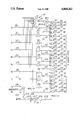
The FIGURE is a schematic diagram of the circuitry for resetting a multi-bit word in a digital memory.
DETAILED DESCRIPTION OF THE INVENTION
This invention is directed to circuitry for invalidating addresses in a memory. It is particularly suited for a digital computer system that uses at least one main memory and at least one associated cache memory. When a processor writes into an address in the main memory, if there is a corresponding address in the cache memory, that cache memory must be earmarked as invalid or the contents must be immediately changed to reflect the data written into the main memory. The practical solution is to invalidate the corresponding cache memory location. This invention makes that function economical in time and circuitry.
Also, in a single memory system, it may be desirable to write data into the memory, read the data, and check its correctness, and if incorrect, to invalidate that data. This invention, of course, permits such an application.
The FIGURE is a schematic diagram of the circuitry in this preferred embodiment that performs the function of invalidating (resetting) a memory location. As mentioned above, in the cache memory system, a portion of an address is actually reset, rather than data at a given address.
The input multi-bit data word is represented as signals D0-D8 which are applied to inverters 20-28. The outputs from inverters 20-22 are input to exclusive-OR circuit 12; the output from inverters 23-25 are input to exclusive-OR circuit 14; the outputs from inverters 26-28 are input to exclusive-OR circuit 16. The outputs from exclusive-OR circuits 12, 14 and 16 are input to exclusive-NOR circuit 18 to provide a parity signal. In this preferred embodiment, an odd parity system is used which is one wherein an odd number of "1's" in the input multi-bit data word will result in a "1" parity bit. This is of course an engineering design choice.
The outputs from inverters 20-28 respectively are input to NOR gates 30-38, respectively. A word RESET-signal from a computer system is applied to inverter 102 whose output is applied to the input of each of NOR gates 30-38, respectively.
The output from inverter 102 is also applied to inverter 90 whose output serves as an input to NAND gate 92. The other input to NAND gate 92 comes from exclusive-NOR gate 18. The word reset signal therefore controls gates 30-38 and 92.
The inputs to inverters 40-48 are connected to the outputs or NOR gates 30-38, respectively. The outputs from NOR-gates 30-38 are also connected as inputs to NAND gates 50-58, respectively. The outputs from inverters 40-48 are connected as inputs to NAND gates 60-68, respectively. The outputs from NAND gates 50-58 are input to inverters 70-78 to provide signals D'0 through D'8, respectively. The outputs from NAND gates 60-68 provide inputs to inverters 80-88, respectively, which in turn provide output signals D'0- through D'8-.
The output from inverter 102 which receives the signal WORD RESET- provides an input to NAND gate 104 whose other input is provided by inverter 103. The input to 103 is the chip select signal CS-, a signal selecting the chip. The output from NAND gate 104 provides one input to NAND gate 105 whose other input is provided by the write command signal WRITE-. The output from NAND gate 105 provides a direct input to NAND gate 108 and also provides an input to inverter D1 whose output is connected to the input of inverter 106 whose output provides an input to inverter 107 whose output provides another input to NAND gate 108. Inverters 106 and 107 provide a delay of the "0" output and NAND gate 108 when the output from NAND gate 105 is a "1". The output from NAND gate 108 is inverted through inverter 109 and is applied to the input of NAND gates 50-68, 91 and 96, respectively.
The output from inverter 103 which is the chip select signal is also applied to the inputs of NAND gate 50-68, 91 and 96, respectively.
The output from NAND gate 92 provides an input to NAND gate 96 via inverter 94 and also an input to NAND gate 91. The output from NAND gate 96 is inverted through inverter 98 and provides signal D'9 and the output from NAND gate 91 is inverted through inverter 92 and provides signal D'9-. Signals D'0 through D'9 and their inverse signals D'0- through D'9- are then written into the digital memory according to the input multi-bit data word D0-D8 or by the reset multi-bit word resulting from gates 30-38 and 92, respectively.
MODE OF OPERATION OF THE INVENTION
When WORD RESET- is high ("1") and signals CS- and WRITE- are both low ("0"), the circuit is in a WRITE mode. A multi-bit input data word, represented by signals D0-D8 are input, inverted and sent to the parity generator made up of exclusive-OR gates 12, 14 and 16, and exclusive-NOR gate 18 to yield a parity bit. At the same time, input signals D0-D8, inverted through inverters 20-28 are input to NOR gates 30-38. The outputs from NOR gates 30-38 are transmitted to NAND gates 50-58, and inverted and sent to the inputs of NAND gates 60-68.
With the WRITE- signal being a "0", the output from NAND gate 105 is a "1" which is immediately applied to the input of NAND gate 108. The output of NAND gate 108 at that time is a "1", resulting in a "0" out of inverter 109, disabling gates 50-68, 91 and 96.
A parity generated out of exclusive-NOR gate 18 is input to NAND gate 92 whose other input is supplied from inverter 90. Since WORD RESET- signal is "1", the output of inverter 102 is a "0" and the output of inverter 90 is a "1", enabling AND gate 92. If, for example, the parity generated is a "1", then a "0" will be output from NAND gate 92, inverted through inverter 94 and presented as a "1" to the input of NAND gate 96. Not inverted, it will appear as a "0" to the input of NAND gate 91.
While these signals were forming in NAND gates 50-68, 91 and 96, the enabling signal from inverter 109 was "0", therefore disabling those gates. The "1" output from NAND gate 105 is inverted through inverter 106 and again through 107 to provide a "1" input to the other input of NAND gate 108. The time taken for the two inversions is sufficient for the information to settle in the gates described above. At that time, a "0" is output from NAND gate 108, inverted through inverted 109 and applied as an enabling input to NAND gates 50-68, 91 and 96. The outputs from those gates are all inverted through inverters 70-88, 92 and 98 to provide outputs D'0 through D'9 and D'0- through D'9-. These signals are then written into the memory.
Now assume that signal WORD RESET- goes to a "0". Then the output from inverter 102 is a "1" that is applied to the inputs of each of gates 30-38, and is also inverted through inverter 90 and applied as an input to NAND gate 92. Under these conditions, NOR gates 30-38 are disabled and NAND gate 92 is disabled. All "0's" out of NOR gates 30-38 are transmitted to NAND gates 50-58 with their reciprocals residing in NAND gates 60-68. At the same time, a "0" on the input to NAND gate 92 from inverter 90 results in a "0" output which is inverted through inverter 94 and presented to the input of NAND gate 96 with a "1" being presented to the input of NAND gate 91.
As in the write operation described earlier, the delayed WRITE signal causes a "1" output from inverter 109, enabling the gates 50-68, 91 and 96 to transmit all "0's" to the memory at the addressed location.
This circuit enables writing a word into memory with its generated parity in a minimum of time. A minimum of time is also required in a practical sense for writing "0's" together with a "0" parity bit and this circuit accomplishes that function as well.
Those skilled in the art realize that this invention may be practices without exactly copying the circuitry as set out in this preferred embodiment. The invention is limited only by the appended claims.

Claims (10)

I claim:
1. A circuit for writing a multi-bit word into a digital memory at a selected address upon receipt of a write command and responsive to a word reset signal for resetting a multi-bit word that includes at least one parity bit in the digital memory at a selected address, comprising:
(a) internal data memory circuit means for receiving a multi-bit word and responsive to reception of said write command to write the multi-bit word into the digital memory at a selected address;
(b) parity generator means connected to receive a multi-bit input data word and to generate at least one parity bit therefrom; and
(c) resetting means responsive to receipt of said multi-bit word, said parity bit, and said word reset signal to write a reset multi-bit word to the internal data memory circuit means, all the bits of said word being set to a predetermined level and the parity bit being set to said predetermined level corresponding to parity for the reset multi-bit word for writing into the digital memory in the presence of the write command.
2. The circuit of claim 1 wherein the internal data memory circuit means comprises a plurality of bus gates.
3. The circuit of claim 2 wherein the plurality of bus gates further comprises a NAND gate for each position of the multi-bit word, including the parity bit, for generating each bit of the reset multi-bit word and the parity bit.
4. The circuit of claim 3 wherein the plurality of bus gates further comprise a second NAND gate for each position for generating the inverse of each bit and the party bit.
5. The circuit of claim 1 wherein the parity generator means comprises exclusive OR gate means for receiving the multi-bit data word, and exclusive NOR gate means for receiving the output of the exclusive OR gate means to provide a parity bit.
6. The circuit of claim 1 wherein the resetting means comprises a NOR gate for each position of the input multi-bit data word and a NAND gate for the parity bit, each of the NOR gates and the NAND gate connected to receive the word reset signal.
7. The circuit of claim 6 further comprising an inverter for inverting the word reset signal to provide an inverted word reset signal to the NAND gate.
8. The circuit of claim 1 wherein the resetting means comprises delay means for receiving and delaying the write signal until the reset multi-bit word and the corresponding parity bit have had time to enter the internal data memory circuit means.
9. The circuit of claim 8 wherein the delay means comprises a pair of inverters connected in series.
10. The circuit of claim 1 wherein each bit of the reset multi-bit word and the parity bit is set to zero.
US07/081,925 1987-08-05 1987-08-05 Cache memory reset responsive to change in main memory Expired - Lifetime US4860262A (en)

Priority Applications (2)

Application Number Priority Date Filing Date Title
US07/081,925 US4860262A (en) 1987-08-05 1987-08-05 Cache memory reset responsive to change in main memory
JP63193577A JP3093761B2 (en) 1987-08-05 1988-08-04 Circuit to reset multi-bit word

Applications Claiming Priority (1)

Application Number Priority Date Filing Date Title
US07/081,925 US4860262A (en) 1987-08-05 1987-08-05 Cache memory reset responsive to change in main memory

Publications (1)

Publication Number Publication Date
US4860262A true US4860262A (en) 1989-08-22

Family

ID=22167277

Family Applications (1)

Application Number Title Priority Date Filing Date
US07/081,925 Expired - Lifetime US4860262A (en) 1987-08-05 1987-08-05 Cache memory reset responsive to change in main memory

Country Status (2)

Country Link
US (1) US4860262A (en)
JP (1) JP3093761B2 (en)

Cited By (4)

* Cited by examiner, † Cited by third party
Publication number Priority date Publication date Assignee Title
US5043943A (en) * 1990-06-18 1991-08-27 Motorola, Inc. Cache memory with a parity write control circuit
US5226009A (en) * 1990-03-30 1993-07-06 Mitsubishi Denki Kabushiki Kaisha Semiconductor memory device supporting cache and method of driving the same
US5719808A (en) * 1989-04-13 1998-02-17 Sandisk Corporation Flash EEPROM system
US6462992B2 (en) 1989-04-13 2002-10-08 Sandisk Corporation Flash EEprom system

Families Citing this family (1)

* Cited by examiner, † Cited by third party
Publication number Priority date Publication date Assignee Title
JPH09293017A (en) * 1996-04-24 1997-11-11 Nec Niigata Ltd Computer

Citations (2)

* Cited by examiner, † Cited by third party
Publication number Priority date Publication date Assignee Title
US4099069A (en) * 1976-10-08 1978-07-04 Westinghouse Electric Corp. Circuit producing a common clear signal for erasing selected arrays in a mnos memory system
US4155070A (en) * 1977-12-01 1979-05-15 Northern Telecom Limited Code-converter with preservation of parity

Family Cites Families (3)

* Cited by examiner, † Cited by third party
Publication number Priority date Publication date Assignee Title
JPS6066384A (en) * 1983-09-21 1985-04-16 Nec Corp Memory control circuit
JPS60236199A (en) * 1984-05-08 1985-11-22 Nec Corp Semiconductor memory device
JPS62154286A (en) * 1985-12-26 1987-07-09 Nec Corp Write access system for rewritable memory

Patent Citations (2)

* Cited by examiner, † Cited by third party
Publication number Priority date Publication date Assignee Title
US4099069A (en) * 1976-10-08 1978-07-04 Westinghouse Electric Corp. Circuit producing a common clear signal for erasing selected arrays in a mnos memory system
US4155070A (en) * 1977-12-01 1979-05-15 Northern Telecom Limited Code-converter with preservation of parity

Cited By (6)

* Cited by examiner, † Cited by third party
Publication number Priority date Publication date Assignee Title
US5719808A (en) * 1989-04-13 1998-02-17 Sandisk Corporation Flash EEPROM system
US5999446A (en) * 1989-04-13 1999-12-07 Sandisk Corporation Multi-state flash EEprom system with selective multi-sector erase
US6462992B2 (en) 1989-04-13 2002-10-08 Sandisk Corporation Flash EEprom system
US7460399B1 (en) 1989-04-13 2008-12-02 Sandisk Corporation Flash EEprom system
US5226009A (en) * 1990-03-30 1993-07-06 Mitsubishi Denki Kabushiki Kaisha Semiconductor memory device supporting cache and method of driving the same
US5043943A (en) * 1990-06-18 1991-08-27 Motorola, Inc. Cache memory with a parity write control circuit

Also Published As

Publication number Publication date
JP3093761B2 (en) 2000-10-03
JPH01111243A (en) 1989-04-27

Similar Documents

Publication Publication Date Title
US5265231A (en) Refresh control arrangement and a method for refreshing a plurality of random access memory banks in a memory system
US3840862A (en) Status indicator apparatus for tag directory in associative stores
US4882709A (en) Conditional write RAM
US4602368A (en) Dual validity bit arrays
US4276609A (en) CCD memory retrieval system
US4797813A (en) Cache memory control apparatus
JPS58212694A (en) Memory system
GB1590198A (en) Data storage
US5619677A (en) Data processing system with an enhanced cache memory control
JPS6259822B2 (en)
US4930106A (en) Dual cache RAM for rapid invalidation
US5675763A (en) Cache memory system and method for selectively removing stale aliased entries
US5319768A (en) Control circuit for resetting a snoop valid bit in a dual port cache tag memory
US4223382A (en) Closed loop error correct
US5835934A (en) Method and apparatus of low power cache operation with a tag hit enablement
US5845317A (en) Multi-way cache expansion circuit architecture
US6591393B1 (en) Masking error detection/correction latency in multilevel cache transfers
EP0506474B1 (en) Parity detect circuit for memory including dual validity indication
US5386528A (en) Address translator having a high speed data comparator
US4344130A (en) Apparatus to execute DMA transfer between computing devices using a block move instruction
US4860262A (en) Cache memory reset responsive to change in main memory
US5396460A (en) FIFO memory in which number of bits subject to each data read/write operation is changeable
US5584003A (en) Control systems having an address conversion device for controlling a cache memory and a cache tag memory
US5008817A (en) Method and apparatus for transferring addresses and information in a buffer memory and a common main storage device
US3631400A (en) Data-processing system having logical storage data register

Legal Events

Date Code Title Description
AS Assignment

Owner name: TEXAS INSTRUMENTS INCORPORATED, 13500 NORTH CENTRA

Free format text: ASSIGNMENT OF ASSIGNORS INTEREST.;ASSIGNOR:CHIU, EDISON H.;REEL/FRAME:004763/0240

Effective date: 19870805

Owner name: TEXAS INSTRUMENTS INCORPORATED,TEXAS

Free format text: ASSIGNMENT OF ASSIGNORS INTEREST;ASSIGNOR:CHIU, EDISON H.;REEL/FRAME:004763/0240

Effective date: 19870805

STCF Information on status: patent grant

Free format text: PATENTED CASE

FEPP Fee payment procedure

Free format text: PAYOR NUMBER ASSIGNED (ORIGINAL EVENT CODE: ASPN); ENTITY STATUS OF PATENT OWNER: LARGE ENTITY

FPAY Fee payment

Year of fee payment: 4

FPAY Fee payment

Year of fee payment: 8

FPAY Fee payment

Year of fee payment: 12