US4862463A - Error correcting code for 8-bit-per-chip memory with reduced redundancy - Google Patents
Error correcting code for 8-bit-per-chip memory with reduced redundancy Download PDFInfo
- Publication number
- US4862463A US4862463A US07/258,080 US25808088A US4862463A US 4862463 A US4862463 A US 4862463A US 25808088 A US25808088 A US 25808088A US 4862463 A US4862463 A US 4862463A
- Authority
- US
- United States
- Prior art keywords
- matrix
- code
- bits
- symbol
- bit
- Prior art date
- Legal status (The legal status is an assumption and is not a legal conclusion. Google has not performed a legal analysis and makes no representation as to the accuracy of the status listed.)
- Expired - Fee Related
Links
Images


Classifications
-
- G—PHYSICS
- G06—COMPUTING; CALCULATING OR COUNTING
- G06F—ELECTRIC DIGITAL DATA PROCESSING
- G06F11/00—Error detection; Error correction; Monitoring
- G06F11/07—Responding to the occurrence of a fault, e.g. fault tolerance
- G06F11/08—Error detection or correction by redundancy in data representation, e.g. by using checking codes
- G06F11/10—Adding special bits or symbols to the coded information, e.g. parity check, casting out 9's or 11's
- G06F11/1008—Adding special bits or symbols to the coded information, e.g. parity check, casting out 9's or 11's in individual solid state devices
- G06F11/1012—Adding special bits or symbols to the coded information, e.g. parity check, casting out 9's or 11's in individual solid state devices using codes or arrangements adapted for a specific type of error
- G06F11/1028—Adjacent errors, e.g. error in n-bit (n>1) wide storage units, i.e. package error
-
- H—ELECTRICITY
- H03—ELECTRONIC CIRCUITRY
- H03M—CODING; DECODING; CODE CONVERSION IN GENERAL
- H03M13/00—Coding, decoding or code conversion, for error detection or error correction; Coding theory basic assumptions; Coding bounds; Error probability evaluation methods; Channel models; Simulation or testing of codes
- H03M13/03—Error detection or forward error correction by redundancy in data representation, i.e. code words containing more digits than the source words
- H03M13/05—Error detection or forward error correction by redundancy in data representation, i.e. code words containing more digits than the source words using block codes, i.e. a predetermined number of check bits joined to a predetermined number of information bits
- H03M13/13—Linear codes
- H03M13/19—Single error correction without using particular properties of the cyclic codes, e.g. Hamming codes, extended or generalised Hamming codes
Definitions
- This invention relates to error detection and correction and in particular to symbol error correction.
- a symbol is a subset of adjacent bits in a data word and the term package error detection and correction is sometimes used.
- this invention relates to reduced redundancy symbol error detection and correction code which has particular application to a memory organized on a b-bit per chip basis where the symbol size is b.
- This invention is a symbol or package error correcting and detecting code having a reduced redundancy.
- An embodiment of the code is shown in connection with four bit-per-chip memories where an SSC-DSD (single symbol correction - double symbol detection) code is shown for 66 data bits with 14 extra bits to form an 80 bit code word. This represents a savings of 2 redundancy bits as compared to the prior art. Thus, there may be two additional data bits in an 80 bit code word.
- SSC-DSD single symbol correction - double symbol detection
- the code according to the invention is formed by first preparing the general form H matrix for a b-bit-per package SSC-DSD code according to the prior art where the symbol size is b, the code length is bN where there are N packages and the number of check bits is r. Then this general form H matrix is converted to a standard form H(s) matrix where the first non-zero b ⁇ b submatrix of each of the N b-column groups of the matrix is the bxb identity matrix.
- the new code is constructed from H(s) by removing the same set of e columns from each b-column group of the H(s) matrix to form an intermediate matrix H(I) where e is the number of reduced bits from the general H matrix SSC-DSD code. Finally, remove the e all zero rows from the matrix H(I) just formed to create a resultant matrix H(r) with symbol size b-e and code length (b-e)N and the number of check bits equal to r-e.
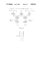
- FIGS. 1A and 1B viewed in left to right relationship, represent an error correction and detection code matrix for producing check bits for a particular example of a code according to the invention.
- FIGS. 2A and 2B viewed in left to right order, represent a resultant matrix for error correction and detection according to the present invention.
- FIG. 3 shows the mapping of bit positions to memory chips for a 4-bit per chip memory using the code shown in FIGS. 2A and 2B for a particular embodiment according to the present invention.
- UEs uncorrectable errors
- FIG. 6B is the logic required to perform the multiplication of the matrix shown in FIG. 6A by the S1 signal as shown in FIG. 4 according to the present invention.
- a computer memory designed with an error correcting code is conventionally organized in a one-bit-per-chip fashion with respect to the ECC words. This organization guarantees that at most one bit of an ECC word would be corrupted by a chip failure.
- the class of SEC-DED (single error correcting and double error detecting) codes are normally used to control the errors in the one-bit-per-chip memory systems.
- the appropriate for a b-bit-per-chip memory design is the class of SSC-DSD codes that can correct all single symbol errors all double symbol errors in an ECC word, where a symbol error is a b-bit error pattern generated from a chip failure.
- An SSC-DSD code is capable of correcting all the errors generated from any single chip failures and detecting all the errors generated from two chip failures.
- a technique is described for the construction of SSC-DSD codes that are more efficient than previous known codes. That is, a new code requires a fewer number of check bits for the same amount of data bits, or a new code can protect more data bits with the same number of check bits as compared to a known SSC-DSD code.
- a comparable new code according to this invention requires only 14 check bits.
- the most efficient known SSC-DSD code can protect 2036 data bits, while a new code according to this invention with 19 check bits can protect 4081 data bits.
- a code word of an SSC-DSD code consists of N b-bit symbols, or bN bits.
- C (C1, C2, . . . , CN) be a code word, where each component Ci, 1 ⁇ i ⁇ N, of C is a symbol of b-bit pattern.
- the code word must satisfy a set of linear equations that can be expressed as:
- C t is the transpose of C
- H the parity check matrix of the code
- bN the parity check matrix of the code
- the code is conventionally denoted as a (bN, bN-r) code, where bN is the code length and bN-r is the number of data bits.
- the symbol weight of a vector is the number of nonzero symbols in the vector.
- the symbol distance of two vectors is the number of symbol positions in which the two vectors are different.
- the minimum symbol distance of a code is the minimum of the symbol distance between any two code words of the code.
- a code is an SSC-DSD code if the minimum symbol distance of the code is equal to or greater than four.
- the parity check matrix of a known code constructed according to the prior art has the following general form: ##EQU1## where each of the b ⁇ b submatrix T ij is either an all zeros matrix or a power of the companion matrix of a primitive polynomial of degree b.
- the companion matrix of the primitive polynomial 1+x+x 4 is: ##EQU2## All 15 distinct powers of this companion matrix are shown in Table 1.
- T 0 is the identity matrix and T* is used to denote the all zeros matrix.
- T -1 T 14
- T -i T 15-i .
- Table 2(B) shows the parity check matrix in standard form to be explained later.
- a word W read from the memory at a particular location may not be the same as the code word C originally written into the same location, because errors may be generated from physical failures.
- the difference between W and C is defined as the error pattern E.
- W C+E
- E i W i -C i for 1 ⁇ i ⁇ N. From (1), we have ##EQU3##
- the vector S is called the error syndrome.
- XOR bit-by-bit exclusive or
- the parity check matrix of an SSC-DSD code with symbol size b and code length bN is said to be in a standard form if the first non-zero bxb submatrix of each of the N b-column groups of the matrix is the b ⁇ b identity matrix. If the parity check matrix H is first generated in the general form of equation (2) above, the matrix can be transformed into a standard form using the following algorithm.
- T ij the smallest integer i, 1 ⁇ i ⁇ R, such that T ij is a non-zero matrix.
- T ij the smallest integer i, 1 ⁇ i ⁇ R, such that T ij is a non-zero matrix.
- T ij the smallest integer i, 1 ⁇ i ⁇ R, such that T ij is a non-zero matrix.
- T ij the smallest integer i, 1 ⁇ i ⁇ R, such that T ij is a non-zero matrix.
- the parity matrix of Table 2(A) can be transformed into a standard form as shown in Table 2(B). If the original parity check matrix defines an SSC-DSD code, the transformed matrix in standard form also defines an SSC-DSD code with the same number of check bits.
- H the parity check matrix of a known (b'N, b'N-r) SSC-DSD code with a symbol size of b'.
- the number of check bits for the code is equal to r.
- H(r) be the final resultant matrix.
- the number of check bits is equal to r-e.
- e can be 1 or greater than 1.
- Table 4 shows the parameters of some new and more efficient SSC-DSD codes that can be constructed from the technique described in this section.
- a memory system is to be organized in 4 bits per chip, and an SSC-DSD code is to be used to protect 66 data bits.
- a previously known code would require 16 check bits. From Table 4, a new code of length 136 with 14 check bits can be constructed. This code can be shortened to protect 66 data bits, resulting in a (80,66) code that saves 2 check bits as compared to the best previously known code. Also for an 80 bit code word, two additional data bits may be provided.
- the parity check matrix of the form (2) can be designed to define an SSC-DSD code with a symbol size of 5.
- the entries of the parity check matrix are powers of T or the 5 ⁇ 5 all zeros matrix. Only 20 of the 34 column groups are selected to form the following matrix.
- H be the 15 ⁇ 100 binary matrix obtained from the mapping of the above matrix according to the following rules: map * into a 5 ⁇ 5 all zeros matrix, and map i into Ti, for 0 ⁇ i ⁇ 30, where T is the matrix of (4).
- the resultant matrix H2 is shown in FIG. 2.
- any set of 14 bit-positions can be designated as the locations of check bits as long as the corresponding 14 columns of H1 form a non-singular matrix, i.e., those 14 columns are linearly independent. Designate positions 1-12, 21 and 30 as ECC check bit positions. Note that each of the first four ECC check bits can be obtained from the parities of two data bytes (the vertical lines in H1 define the data byte boundaries). For example, ECC bit 4 is the sum (XOR) of byte parity of bits 40-48 and the byte parity of bits
- Matrix H1 provides rules for the generation of the fourteen ECC check bits. From (1), the XOR sum of a code word at the positions indicated by the ones in each row of H1 has to be equal to 0. Thus, the rows of H1 define 14 equations that a code word has to satisfy.
- the ECC check bits are derived from these equations. For example, check bit 5 is the XOR sum of data bits at positions 15, 17, 19, 20, 23, 26-28, 35, 38-40, 43, 46, 48, 51, 52, 55, 56, 58, 61, 66, 68, 72, 78 and 79.
- the syndrome of a code word read from the memory is the XOR of the ECC bits read directly from the memory and the ECC bits generated from the data read from the memory. It can be verified that the syndromes of errors in all single chips are nonzero and distinct and the syndromes of errors in all double chips are not the same as any one of the correctable error syndromes.
- the fourteen syndrome bits are all zeros, no error is assumed. If the syndrome is nonzero, there are errors in the code word. In this case, the chip positions and bit positions of the errors have to be identified. All double chip errors and some multiple chip errors will be detected as UE (uncorrectable errors). In the following description, the first four bits of the syndrome are called S1 and the last ten bits of the syndrome are called S2.
- the matrix of FIG. 2 is used for processing the syndrome in error correction.
- the matrix is divided into 20 submatrices, one for each chip, of four columns.
- H(i) is multiplied by S1
- the resultant ten bit pattern is compared with S2. If there is a total agreement, chip i is in error and S1 is the four bit error pattern within chip i. If there is a disagreement, then chip i is error-free.
- FIG. 3 shows the assignment of code word bit positions to chips for this embodiment.
- FIG. 5 shows the logic for chips 2 and 3. If the syndrome is nonzero and there is no error indicator in each of the twenty chips, then the UE signal should be on for an uncorrectable error.
- the multiplication H(i) by S1 can be implemented with an XOR tree.
- the 1-10 individual output bits are shown at the bottom of the XOR blocks while the 1-4 input bits are shown at the top.
Abstract
Description
H·C.sup.t =0mod 2, (1)
__________________________________________________________________________
0 * * 0 0 0 0 0 0 0 0 0 0 0 0 0 0 0 0 0
* 0 * 2 4 1 5 6 17
                  7 16
                      8 0 3 30
                              29
                                18
                                  28
                                    19 27
* * 0 2 0 3 30
              29
                18
                  28
                    19
                      27
                        4 1 5 6 17
                                  7 16 8
__________________________________________________________________________
              TABLE 1
______________________________________
Powers Of The Companion Matrix Of 1 + x + x.sup.4
______________________________________
 ##STR1##
                   ##STR2##
 ##STR3##
                   ##STR4##
 ##STR5##
                   ##STR6##
 ##STR7##
                   ##STR8##
 ##STR9##
                   ##STR10##
 ##STR11##
                   ##STR12##
 ##STR13##
                   ##STR14##
 ##STR15##
                   ##STR16##
______________________________________
              TABLE 2
______________________________________
Parity Check Matrix Of A (44,32) SSC-DSD Code With b = 4
______________________________________
(A) General Form
     I     O      O   I   T.sup.1
                               T.sup.2
                                   T.sup.3
                                        T.sup.4
                                            T.sup.5
                                                 T.sup.6
                                                      T.sup.7
H =  O     I      O   I   T.sup.2
                               T.sup.4
                                   T.sup.6
                                        T.sup.8
                                            T.sup.10
                                                 T.sup.12
                                                      T.sup.14
     O     O      I   I   T.sup.3
                               T.sup.6
                                   T.sup.9
                                        T.sup.12
                                            I    T.sup.3
                                                      T.sup.6
(B) Standard Form
     I     O      O   I   I    I   I    I   I    I    I
H =  O     I      O   I   T.sup.1
                               T.sup.2
                                   T.sup.3
                                        T.sup.4
                                            T.sup.5
                                                 T.sup.6
                                                      T.sup.7
     O     O      I   I   T.sup.2
                               T.sup.4
                                   T.sup.6
                                        T.sup.8
                                            T.sup.10
                                                 T.sup.12
                                                      T.sup.14
______________________________________
              TABLE 3
______________________________________
Parity Check Matrix Of A (33,21) SSC-DSD Code With b = 3
______________________________________
100 000
       000    100    100 100
                            100  100  100  100  100
010 000
       000    010    010 010
                            010  010  010  010  010
001 000
       000    001    001 001
                            001  001  001  001  001
000 100
       000    100    000 001
                            010  100  001  011  110
000 010
       000    010    100 001
                            011  110  101  010  101
000 001
       000    001    010 100
                            001  011  110  101  010
000 000
       000    000    001 010
                            100  001  011  110  101
000 000
       100    100    001 100
                            011  101  101  111  110
000 000
       010    010    001 110
                            010  011  111  100  001
000 000
       001    001    100 011
                            101  101  111  110  000
000 000
       000    000    010 001
                            110  010  011  111  100
______________________________________
              TABLE 4
______________________________________
Parameters of Some New SSC-DSD Codes
No. of  Symbol    Code Length of
                                Code Length of
Check Bits
        Size b    Best Known Codes
                                New Codes
______________________________________
14      4         18 × 4  34 × 4
15      3         133 × 3 257 × 3
18      3         650 × 3 1025 × 3
19      4         257 × 4 1025 × 4
______________________________________
Claims (5)
Priority Applications (1)
| Application Number | Priority Date | Filing Date | Title |
|---|---|---|---|
| US07/258,080 US4862463A (en) | 1987-07-20 | 1988-10-17 | Error correcting code for 8-bit-per-chip memory with reduced redundancy |
Applications Claiming Priority (2)
| Application Number | Priority Date | Filing Date | Title |
|---|---|---|---|
| US7539087A | 1987-07-20 | 1987-07-20 | |
| US07/258,080 US4862463A (en) | 1987-07-20 | 1988-10-17 | Error correcting code for 8-bit-per-chip memory with reduced redundancy |
Related Parent Applications (1)
| Application Number | Title | Priority Date | Filing Date |
|---|---|---|---|
| US7539087A Continuation | 1987-07-20 | 1987-07-20 |
Publications (1)
| Publication Number | Publication Date |
|---|---|
| US4862463A true US4862463A (en) | 1989-08-29 |
Family
ID=26756790
Family Applications (1)
| Application Number | Title | Priority Date | Filing Date |
|---|---|---|---|
| US07/258,080 Expired - Fee Related US4862463A (en) | 1987-07-20 | 1988-10-17 | Error correcting code for 8-bit-per-chip memory with reduced redundancy |
Country Status (1)
| Country | Link |
|---|---|
| US (1) | US4862463A (en) |
Cited By (37)
| Publication number | Priority date | Publication date | Assignee | Title |
|---|---|---|---|---|
| US4961193A (en) * | 1988-04-29 | 1990-10-02 | International Business Machines | Extended errors correcting device having single package error correcting and double package error detecting codes |
| US5164944A (en) * | 1990-06-08 | 1992-11-17 | Unisys Corporation | Method and apparatus for effecting multiple error correction in a computer memory |
| US5226043A (en) * | 1990-12-27 | 1993-07-06 | Raytheon Company | Apparatus and method for data error detection and correction and address error detection in a memory system |
| US5450423A (en) * | 1991-03-19 | 1995-09-12 | Hitachi, Ltd. | Data error correcting/detecting system and apparatus compatible with different data bit memory packages |
| US5600659A (en) * | 1989-03-06 | 1997-02-04 | International Business Machines Corporation | Low cost symbol error correction coding and decoding |
| US5691996A (en) * | 1995-12-11 | 1997-11-25 | International Business Machines Corporation | Memory implemented error detection and correction code with address parity bits |
| US5745507A (en) * | 1995-03-31 | 1998-04-28 | International Business Machines Corporation | Systematic symbol level ECC for use in digital memory systems |
| US5761221A (en) * | 1995-12-11 | 1998-06-02 | International Business Machines Corporation | Memory implemented error detection and correction code using memory modules |
| US5768294A (en) * | 1995-12-11 | 1998-06-16 | International Business Machines Corporation | Memory implemented error detection and correction code capable of detecting errors in fetching data from a wrong address |
| US5909541A (en) * | 1993-07-14 | 1999-06-01 | Honeywell Inc. | Error detection and correction for data stored across multiple byte-wide memory devices |
| US6457154B1 (en) | 1999-11-30 | 2002-09-24 | International Business Machines Corporation | Detecting address faults in an ECC-protected memory |
| US6460157B1 (en) | 1999-11-30 | 2002-10-01 | International Business Machines Corporation | Method system and program products for error correction code conversion |
| FR2823035A1 (en) * | 2001-04-03 | 2002-10-04 | St Microelectronics Sa | Method regarding codes for detecting and/or correcting errors with high efficiency, for use in storage and transmission of data |
| US6463563B1 (en) | 1999-11-30 | 2002-10-08 | International Business Machines Corporation | Single symbol correction double symbol detection code employing a modular H-matrix |
| US20020194530A1 (en) * | 1997-09-30 | 2002-12-19 | Santeler Paul A. | Fault tolerant memory |
| US6519736B1 (en) | 1999-11-30 | 2003-02-11 | International Business Machines Corporation | Generating special uncorrectable error codes for failure isolation |
| US20030070133A1 (en) * | 2001-10-05 | 2003-04-10 | Bauman Mitchell A. | Familial correction with non-familial double bit error detection |
| US20040064776A1 (en) * | 2002-09-30 | 2004-04-01 | Yedidia Jonathan S. | Transforming generalized parity check matrices for error-correcting codes |
| US6751769B2 (en) | 2000-06-06 | 2004-06-15 | International Business Machines Corporation | (146,130) error correction code utilizing address information |
| US20050149834A1 (en) * | 2003-12-23 | 2005-07-07 | International Business Machines Corporation | (18, 9) Error correction code for double error correction and triple error detection |
| US20050188292A1 (en) * | 2003-12-23 | 2005-08-25 | International Business Machines Corporation | Method and apparatus for encoding special uncorrectable errors in an error correction code |
| US20050246615A1 (en) * | 2002-07-02 | 2005-11-03 | Wataru Matsumoto | Check matrix generation method and check matrix generation device |
| US20050249010A1 (en) * | 2004-05-06 | 2005-11-10 | Klein Dean A | Memory controller method and system compensating for memory cell data losses |
| US6965537B1 (en) | 2004-08-31 | 2005-11-15 | Micron Technology, Inc. | Memory system and method using ECC to achieve low power refresh |
| US20050289444A1 (en) * | 2004-06-25 | 2005-12-29 | Klein Dean A | Low power cost-effective ECC memory system and method |
| US20060010339A1 (en) * | 2004-06-24 | 2006-01-12 | Klein Dean A | Memory system and method having selective ECC during low power refresh |
| US20060013052A1 (en) * | 2004-07-15 | 2006-01-19 | Klein Dean A | Method and system for controlling refresh to avoid memory cell data losses |
| US20070011598A1 (en) * | 2005-06-15 | 2007-01-11 | Hitachi Global Storage Technologies Netherlands B.V. | Error detection and correction for encoded data |
| US20070283208A1 (en) * | 2006-06-01 | 2007-12-06 | International Business Machines Corporation | Systems, methods, and computer program products for providing a two-bit symbol bus error correcting code with bus diagnostic features |
| US20070283223A1 (en) * | 2006-06-01 | 2007-12-06 | International Business Machines Corporation | Systems, methods, and computer program products for providing a two-bit symbol bus error correcting code with all checkbits transferred last |
| US20070283229A1 (en) * | 2006-06-01 | 2007-12-06 | International Business Machines Corporation | Systems, methods, and computer program products for providing a two-bit symbol bus error correcting code |
| US20070283207A1 (en) * | 2006-06-01 | 2007-12-06 | International Business Machines Corporation | Systems, methods, and computer program products for providing a two-bit symbol bus error correcting code with bus timing improvements |
| US20080096631A1 (en) * | 2004-10-02 | 2008-04-24 | Wms Gaming Inc. | Gaming Device With Error Correcting Memory |
| US20080184093A1 (en) * | 2007-01-26 | 2008-07-31 | Thayer Larry J | Error correction algorithm selection based upon memory organization |
| US7894289B2 (en) | 2006-10-11 | 2011-02-22 | Micron Technology, Inc. | Memory system and method using partial ECC to achieve low power refresh and fast access to data |
| US7900120B2 (en) | 2006-10-18 | 2011-03-01 | Micron Technology, Inc. | Memory system and method using ECC with flag bit to identify modified data |
| US9997233B1 (en) | 2015-10-08 | 2018-06-12 | Rambus Inc. | Memory module with dynamic stripe width |
Citations (11)
| Publication number | Priority date | Publication date | Assignee | Title |
|---|---|---|---|---|
| US3623155A (en) * | 1969-12-24 | 1971-11-23 | Ibm | Optimum apparatus and method for check bit generation and error detection, location and correction |
| US3629824A (en) * | 1970-02-12 | 1971-12-21 | Ibm | Apparatus for multiple-error correcting codes |
| US3634821A (en) * | 1970-04-13 | 1972-01-11 | Ibm | Error correcting system |
| US3745525A (en) * | 1971-12-15 | 1973-07-10 | Ibm | Error correcting system |
| US3755779A (en) * | 1971-12-14 | 1973-08-28 | Ibm | Error correction system for single-error correction, related-double-error correction and unrelated-double-error detection |
| US4464753A (en) * | 1981-12-30 | 1984-08-07 | International Business Machines Corporation | Two bit symbol SEC/DED code |
| US4509172A (en) * | 1982-09-28 | 1985-04-02 | International Business Machines Corporation | Double error correction - triple error detection code |
| US4617664A (en) * | 1984-06-29 | 1986-10-14 | International Business Machines Corporation | Error correction for multiple bit output chips |
| US4651321A (en) * | 1983-08-29 | 1987-03-17 | Amdahl Corporation | Apparatus for reducing storage necessary for error correction and detection in data processing machines |
| US4661955A (en) * | 1985-01-18 | 1987-04-28 | Ibm Corporation | Extended error correction for package error correction codes |
| US4713816A (en) * | 1986-02-25 | 1987-12-15 | U.S. Philips Corporation | Three module memory system constructed with symbol-wide memory chips and having an error protection feature, each symbol consisting of 2I+1 bits |
-
1988
- 1988-10-17 US US07/258,080 patent/US4862463A/en not_active Expired - Fee Related
Patent Citations (11)
| Publication number | Priority date | Publication date | Assignee | Title |
|---|---|---|---|---|
| US3623155A (en) * | 1969-12-24 | 1971-11-23 | Ibm | Optimum apparatus and method for check bit generation and error detection, location and correction |
| US3629824A (en) * | 1970-02-12 | 1971-12-21 | Ibm | Apparatus for multiple-error correcting codes |
| US3634821A (en) * | 1970-04-13 | 1972-01-11 | Ibm | Error correcting system |
| US3755779A (en) * | 1971-12-14 | 1973-08-28 | Ibm | Error correction system for single-error correction, related-double-error correction and unrelated-double-error detection |
| US3745525A (en) * | 1971-12-15 | 1973-07-10 | Ibm | Error correcting system |
| US4464753A (en) * | 1981-12-30 | 1984-08-07 | International Business Machines Corporation | Two bit symbol SEC/DED code |
| US4509172A (en) * | 1982-09-28 | 1985-04-02 | International Business Machines Corporation | Double error correction - triple error detection code |
| US4651321A (en) * | 1983-08-29 | 1987-03-17 | Amdahl Corporation | Apparatus for reducing storage necessary for error correction and detection in data processing machines |
| US4617664A (en) * | 1984-06-29 | 1986-10-14 | International Business Machines Corporation | Error correction for multiple bit output chips |
| US4661955A (en) * | 1985-01-18 | 1987-04-28 | Ibm Corporation | Extended error correction for package error correction codes |
| US4713816A (en) * | 1986-02-25 | 1987-12-15 | U.S. Philips Corporation | Three module memory system constructed with symbol-wide memory chips and having an error protection feature, each symbol consisting of 2I+1 bits |
Non-Patent Citations (6)
| Title |
|---|
| Ibid. vol. 24, No. 10, Mar. 1982, "Optimized Error Correction/Detection for Chips . . . By-1", by W. H. Cochran et al, pp. 5275-5276. |
| Ibid. vol. 24, No. 10, Mar. 1982, Optimized Error Correction/Detection for Chips . . . By 1 , by W. H. Cochran et al, pp. 5275 5276. * |
| Ibid. vol. 28, No. 1, Jun. 1985, "Dual Mode Error Correction and Detection", by C. L. Chen, pp. 55-58. |
| Ibid. vol. 28, No. 1, Jun. 1985, Dual Mode Error Correction and Detection , by C. L. Chen, pp. 55 58. * |
| IBM Technical Disclosure Bulletin Article: vol. 22, No. 6, Nov. 1979; "SEC-DED Codes with Package Error Detection Ability"; by C. L. Chen, pp. 2356-2359. |
| IBM Technical Disclosure Bulletin Article: vol. 22, No. 6, Nov. 1979; SEC DED Codes with Package Error Detection Ability ; by C. L. Chen, pp. 2356 2359. * |
Cited By (82)
| Publication number | Priority date | Publication date | Assignee | Title |
|---|---|---|---|---|
| US4961193A (en) * | 1988-04-29 | 1990-10-02 | International Business Machines | Extended errors correcting device having single package error correcting and double package error detecting codes |
| US5600659A (en) * | 1989-03-06 | 1997-02-04 | International Business Machines Corporation | Low cost symbol error correction coding and decoding |
| US5164944A (en) * | 1990-06-08 | 1992-11-17 | Unisys Corporation | Method and apparatus for effecting multiple error correction in a computer memory |
| US5226043A (en) * | 1990-12-27 | 1993-07-06 | Raytheon Company | Apparatus and method for data error detection and correction and address error detection in a memory system |
| US5450423A (en) * | 1991-03-19 | 1995-09-12 | Hitachi, Ltd. | Data error correcting/detecting system and apparatus compatible with different data bit memory packages |
| US5909541A (en) * | 1993-07-14 | 1999-06-01 | Honeywell Inc. | Error detection and correction for data stored across multiple byte-wide memory devices |
| US5745507A (en) * | 1995-03-31 | 1998-04-28 | International Business Machines Corporation | Systematic symbol level ECC for use in digital memory systems |
| US5761221A (en) * | 1995-12-11 | 1998-06-02 | International Business Machines Corporation | Memory implemented error detection and correction code using memory modules |
| US5768294A (en) * | 1995-12-11 | 1998-06-16 | International Business Machines Corporation | Memory implemented error detection and correction code capable of detecting errors in fetching data from a wrong address |
| US5691996A (en) * | 1995-12-11 | 1997-11-25 | International Business Machines Corporation | Memory implemented error detection and correction code with address parity bits |
| US20020194530A1 (en) * | 1997-09-30 | 2002-12-19 | Santeler Paul A. | Fault tolerant memory |
| US7409581B2 (en) * | 1997-09-30 | 2008-08-05 | Hewlett-Packard Development Company, L.P. | Main memory controller adapted to correct corrupted data by xoring corrupted data to directly generate correct data |
| US6457154B1 (en) | 1999-11-30 | 2002-09-24 | International Business Machines Corporation | Detecting address faults in an ECC-protected memory |
| US6460157B1 (en) | 1999-11-30 | 2002-10-01 | International Business Machines Corporation | Method system and program products for error correction code conversion |
| US6463563B1 (en) | 1999-11-30 | 2002-10-08 | International Business Machines Corporation | Single symbol correction double symbol detection code employing a modular H-matrix |
| US6519736B1 (en) | 1999-11-30 | 2003-02-11 | International Business Machines Corporation | Generating special uncorrectable error codes for failure isolation |
| US6751769B2 (en) | 2000-06-06 | 2004-06-15 | International Business Machines Corporation | (146,130) error correction code utilizing address information |
| FR2823035A1 (en) * | 2001-04-03 | 2002-10-04 | St Microelectronics Sa | Method regarding codes for detecting and/or correcting errors with high efficiency, for use in storage and transmission of data |
| US20030046635A1 (en) * | 2001-04-03 | 2003-03-06 | Stmicroelectronics S.A. | High-efficiency error detection and/or correction code |
| US7203896B2 (en) | 2001-04-03 | 2007-04-10 | Stmicroelectronics S.A. | High-efficiency error detection and/or correction code |
| US20030070133A1 (en) * | 2001-10-05 | 2003-04-10 | Bauman Mitchell A. | Familial correction with non-familial double bit error detection |
| US7634709B2 (en) * | 2001-10-05 | 2009-12-15 | Unisys Corporation | Familial correction with non-familial double bit error detection |
| US20050246615A1 (en) * | 2002-07-02 | 2005-11-03 | Wataru Matsumoto | Check matrix generation method and check matrix generation device |
| US7395484B2 (en) * | 2002-07-02 | 2008-07-01 | Mitsubishi Denki Kabushiki Kaisha | Check matrix generation method and check matrix generation device |
| US20040064776A1 (en) * | 2002-09-30 | 2004-04-01 | Yedidia Jonathan S. | Transforming generalized parity check matrices for error-correcting codes |
| US7103818B2 (en) * | 2002-09-30 | 2006-09-05 | Mitsubishi Electric Research Laboratories, Inc | Transforming generalized parity check matrices for error-correcting codes |
| US7243293B2 (en) | 2003-12-23 | 2007-07-10 | International Business Machines Corporation | (18, 9) Error correction code for double error correction and triple error detection |
| US20050149834A1 (en) * | 2003-12-23 | 2005-07-07 | International Business Machines Corporation | (18, 9) Error correction code for double error correction and triple error detection |
| US20050188292A1 (en) * | 2003-12-23 | 2005-08-25 | International Business Machines Corporation | Method and apparatus for encoding special uncorrectable errors in an error correction code |
| US7171591B2 (en) | 2003-12-23 | 2007-01-30 | International Business Machines Corporation | Method and apparatus for encoding special uncorrectable errors in an error correction code |
| US7836374B2 (en) | 2004-05-06 | 2010-11-16 | Micron Technology, Inc. | Memory controller method and system compensating for memory cell data losses |
| US7447973B2 (en) | 2004-05-06 | 2008-11-04 | Micron Technology, Inc. | Memory controller method and system compensating for memory cell data losses |
| US7099221B2 (en) | 2004-05-06 | 2006-08-29 | Micron Technology, Inc. | Memory controller method and system compensating for memory cell data losses |
| US20050249010A1 (en) * | 2004-05-06 | 2005-11-10 | Klein Dean A | Memory controller method and system compensating for memory cell data losses |
| US9064600B2 (en) | 2004-05-06 | 2015-06-23 | Micron Technology, Inc. | Memory controller method and system compensating for memory cell data losses |
| US8689077B2 (en) | 2004-05-06 | 2014-04-01 | Micron Technology, Inc. | Memory controller method and system compensating for memory cell data losses |
| US7428687B2 (en) | 2004-05-06 | 2008-09-23 | Micron Technology, Inc. | Memory controller method and system compensating for memory cell data losses |
| US20060069856A1 (en) * | 2004-05-06 | 2006-03-30 | Klein Dean A | Memory controller method and system compensating for memory cell data losses |
| US7447974B2 (en) | 2004-05-06 | 2008-11-04 | Micron Technology, Inc. | Memory controller method and system compensating for memory cell data losses |
| US7461320B2 (en) | 2004-06-24 | 2008-12-02 | Micron Technology, Inc. | Memory system and method having selective ECC during low power refresh |
| US20060010339A1 (en) * | 2004-06-24 | 2006-01-12 | Klein Dean A | Memory system and method having selective ECC during low power refresh |
| US20050289444A1 (en) * | 2004-06-25 | 2005-12-29 | Klein Dean A | Low power cost-effective ECC memory system and method |
| US7340668B2 (en) | 2004-06-25 | 2008-03-04 | Micron Technology, Inc. | Low power cost-effective ECC memory system and method |
| US7526713B2 (en) | 2004-06-25 | 2009-04-28 | Micron Technology, Inc. | Low power cost-effective ECC memory system and method |
| US20060218469A1 (en) * | 2004-06-25 | 2006-09-28 | Klein Dean A | Low power cost-effective ECC memory system and method |
| US7272066B2 (en) | 2004-07-15 | 2007-09-18 | Micron Technology, Inc. | Method and system for controlling refresh to avoid memory cell data losses |
| US7558142B2 (en) | 2004-07-15 | 2009-07-07 | Micron Technology, Inc. | Method and system for controlling refresh to avoid memory cell data losses |
| US20060152989A1 (en) * | 2004-07-15 | 2006-07-13 | Klein Dean A | Method and system for controlling refresh to avoid memory cell data losses |
| US8446783B2 (en) | 2004-07-15 | 2013-05-21 | Micron Technology, Inc. | Digit line comparison circuits |
| US8279683B2 (en) | 2004-07-15 | 2012-10-02 | Micron Technology, Inc. | Digit line comparison circuits |
| US7898892B2 (en) | 2004-07-15 | 2011-03-01 | Micron Technology, Inc. | Method and system for controlling refresh to avoid memory cell data losses |
| US20060158950A1 (en) * | 2004-07-15 | 2006-07-20 | Klein Dean A | Method and system for controlling refresh to avoid memory cell data losses |
| US7280386B2 (en) | 2004-07-15 | 2007-10-09 | Micron Technology, Inc. | Method and system for controlling refresh to avoid memory cell data losses |
| US7277345B2 (en) | 2004-07-15 | 2007-10-02 | Micron Technology, Inc. | Method and system for controlling refresh to avoid memory cell data losses |
| US20060013052A1 (en) * | 2004-07-15 | 2006-01-19 | Klein Dean A | Method and system for controlling refresh to avoid memory cell data losses |
| US7116602B2 (en) | 2004-07-15 | 2006-10-03 | Micron Technology, Inc. | Method and system for controlling refresh to avoid memory cell data losses |
| US7623392B2 (en) | 2004-07-15 | 2009-11-24 | Micron Technology, Inc. | Method and system for controlling refresh to avoid memory cell data losses |
| US6965537B1 (en) | 2004-08-31 | 2005-11-15 | Micron Technology, Inc. | Memory system and method using ECC to achieve low power refresh |
| US7184352B2 (en) | 2004-08-31 | 2007-02-27 | Micron Technology, Inc. | Memory system and method using ECC to achieve low power refresh |
| US20060044913A1 (en) * | 2004-08-31 | 2006-03-02 | Klein Dean A | Memory system and method using ECC to achieve low power refresh |
| US20080096631A1 (en) * | 2004-10-02 | 2008-04-24 | Wms Gaming Inc. | Gaming Device With Error Correcting Memory |
| US7653862B2 (en) * | 2005-06-15 | 2010-01-26 | Hitachi Global Storage Technologies Netherlands B.V. | Error detection and correction for encoded data |
| US20070011598A1 (en) * | 2005-06-15 | 2007-01-11 | Hitachi Global Storage Technologies Netherlands B.V. | Error detection and correction for encoded data |
| US20070283229A1 (en) * | 2006-06-01 | 2007-12-06 | International Business Machines Corporation | Systems, methods, and computer program products for providing a two-bit symbol bus error correcting code |
| US7721178B2 (en) | 2006-06-01 | 2010-05-18 | International Business Machines Corporation | Systems, methods, and computer program products for providing a two-bit symbol bus error correcting code |
| US20070283208A1 (en) * | 2006-06-01 | 2007-12-06 | International Business Machines Corporation | Systems, methods, and computer program products for providing a two-bit symbol bus error correcting code with bus diagnostic features |
| US20070283207A1 (en) * | 2006-06-01 | 2007-12-06 | International Business Machines Corporation | Systems, methods, and computer program products for providing a two-bit symbol bus error correcting code with bus timing improvements |
| US20070283223A1 (en) * | 2006-06-01 | 2007-12-06 | International Business Machines Corporation | Systems, methods, and computer program products for providing a two-bit symbol bus error correcting code with all checkbits transferred last |
| US7894289B2 (en) | 2006-10-11 | 2011-02-22 | Micron Technology, Inc. | Memory system and method using partial ECC to achieve low power refresh and fast access to data |
| US8832522B2 (en) | 2006-10-11 | 2014-09-09 | Micron Technology, Inc. | Memory system and method using partial ECC to achieve low power refresh and fast access to data |
| US9286161B2 (en) | 2006-10-11 | 2016-03-15 | Micron Technology, Inc. | Memory system and method using partial ECC to achieve low power refresh and fast access to data |
| US8359517B2 (en) | 2006-10-11 | 2013-01-22 | Micron Technology, Inc. | Memory system and method using partial ECC to achieve low power refresh and fast access to data |
| US8880974B2 (en) | 2006-10-18 | 2014-11-04 | Micron Technology, Inc. | Memory system and method using ECC with flag bit to identify modified data |
| US7900120B2 (en) | 2006-10-18 | 2011-03-01 | Micron Technology, Inc. | Memory system and method using ECC with flag bit to identify modified data |
| US8601341B2 (en) | 2006-10-18 | 2013-12-03 | Micron Technologies, Inc. | Memory system and method using ECC with flag bit to identify modified data |
| US8413007B2 (en) | 2006-10-18 | 2013-04-02 | Micron Technology, Inc. | Memory system and method using ECC with flag bit to identify modified data |
| US7975205B2 (en) | 2007-01-26 | 2011-07-05 | Hewlett-Packard Development Company, L.P. | Error correction algorithm selection based upon memory organization |
| US20080184093A1 (en) * | 2007-01-26 | 2008-07-31 | Thayer Larry J | Error correction algorithm selection based upon memory organization |
| US9997233B1 (en) | 2015-10-08 | 2018-06-12 | Rambus Inc. | Memory module with dynamic stripe width |
| US10734064B1 (en) | 2015-10-08 | 2020-08-04 | Rambus Inc. | Controlling a dynamic-stripe-width memory module |
| US11264085B1 (en) | 2015-10-08 | 2022-03-01 | Rambus Inc. | Memory component for deployment in a dynamic stripe width memory system |
| US11862236B1 (en) | 2015-10-08 | 2024-01-02 | Rambus Inc. | Memory component for deployment in a dynamic stripe width memory system |
Similar Documents
| Publication | Publication Date | Title |
|---|---|---|
| US4862463A (en) | Error correcting code for 8-bit-per-chip memory with reduced redundancy | |
| US4464753A (en) | Two bit symbol SEC/DED code | |
| US5418796A (en) | Synergistic multiple bit error correction for memory of array chips | |
| US4277844A (en) | Method of detecting and correcting errors in digital data storage systems | |
| US7370264B2 (en) | H-matrix for error correcting circuitry | |
| US5226043A (en) | Apparatus and method for data error detection and correction and address error detection in a memory system | |
| US4589112A (en) | System for multiple error detection with single and double bit error correction | |
| EP0052216B1 (en) | Data storage systems | |
| US4334309A (en) | Error correcting code system | |
| US5856987A (en) | Encoder and decoder for an SEC-DED-S4ED rotational code | |
| US4631725A (en) | Error correcting and detecting system | |
| US5751744A (en) | Error detection and correction circuit | |
| JPS5960654A (en) | Error correction system | |
| US5537423A (en) | Modular multiple error correcting code system | |
| EP0300139B1 (en) | Error correcting code for b-bit-per-chip memory with reduced redundancy | |
| US7028248B2 (en) | Multi-cycle symbol level error correction and memory system | |
| US5450423A (en) | Data error correcting/detecting system and apparatus compatible with different data bit memory packages | |
| US6539513B1 (en) | Dual functioning symbol error correction code | |
| US7721177B2 (en) | Device and method for determining a position of a bit error in a bit sequence | |
| US5425038A (en) | Error plus single bit error detection | |
| US5761221A (en) | Memory implemented error detection and correction code using memory modules | |
| US4888774A (en) | Error detection system | |
| US6463563B1 (en) | Single symbol correction double symbol detection code employing a modular H-matrix | |
| Fujiwara et al. | A class of error-locating codes for byte-organized memory systems | |
| EP0097159B1 (en) | Two bit per symbol sec/ded code |
Legal Events
| Date | Code | Title | Description |
|---|---|---|---|
| FPAY | Fee payment |
Year of fee payment: 4 |
|
| FEPP | Fee payment procedure |
Free format text: PAYOR NUMBER ASSIGNED (ORIGINAL EVENT CODE: ASPN); ENTITY STATUS OF PATENT OWNER: LARGE ENTITY |
|
| FPAY | Fee payment |
Year of fee payment: 8 |
|
| FEPP | Fee payment procedure |
Free format text: PAYOR NUMBER ASSIGNED (ORIGINAL EVENT CODE: ASPN); ENTITY STATUS OF PATENT OWNER: LARGE ENTITY Free format text: PAYER NUMBER DE-ASSIGNED (ORIGINAL EVENT CODE: RMPN); ENTITY STATUS OF PATENT OWNER: LARGE ENTITY |
|
| REMI | Maintenance fee reminder mailed | ||
| LAPS | Lapse for failure to pay maintenance fees | ||
| FP | Lapsed due to failure to pay maintenance fee |
Effective date: 20010829 |
|
| STCH | Information on status: patent discontinuation |
Free format text: PATENT EXPIRED DUE TO NONPAYMENT OF MAINTENANCE FEES UNDER 37 CFR 1.362 |