US4864636A - Crystal controlled transmitter - Google Patents
Crystal controlled transmitter Download PDFInfo
- Publication number
- US4864636A US4864636A US07/016,561 US1656187A US4864636A US 4864636 A US4864636 A US 4864636A US 1656187 A US1656187 A US 1656187A US 4864636 A US4864636 A US 4864636A
- Authority
- US
- United States
- Prior art keywords
- coupled
- frequency
- inductor
- harmonic
- capacitor
- Prior art date
- Legal status (The legal status is an assumption and is not a legal conclusion. Google has not performed a legal analysis and makes no representation as to the accuracy of the status listed.)
- Expired - Lifetime
Links
- 239000013078 crystal Substances 0.000 title claims abstract description 33
- 239000003990 capacitor Substances 0.000 claims description 21
- 230000008878 coupling Effects 0.000 claims description 10
- 238000010168 coupling process Methods 0.000 claims description 10
- 238000005859 coupling reaction Methods 0.000 claims description 10
- 239000004020 conductor Substances 0.000 claims description 8
- 230000003071 parasitic effect Effects 0.000 claims description 3
- 230000005540 biological transmission Effects 0.000 description 7
- 238000010276 construction Methods 0.000 description 6
- 238000013461 design Methods 0.000 description 4
- 238000010586 diagram Methods 0.000 description 4
- 230000010355 oscillation Effects 0.000 description 4
- 238000004806 packaging method and process Methods 0.000 description 4
- 230000008901 benefit Effects 0.000 description 3
- 235000014676 Phragmites communis Nutrition 0.000 description 2
- 229910052790 beryllium Inorganic materials 0.000 description 2
- ATBAMAFKBVZNFJ-UHFFFAOYSA-N beryllium atom Chemical compound [Be] ATBAMAFKBVZNFJ-UHFFFAOYSA-N 0.000 description 2
- 239000000463 material Substances 0.000 description 2
- 230000010363 phase shift Effects 0.000 description 2
- 230000008859 change Effects 0.000 description 1
- 238000001514 detection method Methods 0.000 description 1
- 238000000605 extraction Methods 0.000 description 1
- 238000009434 installation Methods 0.000 description 1
- 230000002452 interceptive effect Effects 0.000 description 1
- 238000012986 modification Methods 0.000 description 1
- 230000004048 modification Effects 0.000 description 1
- 238000012544 monitoring process Methods 0.000 description 1
- 238000012545 processing Methods 0.000 description 1
- 230000005855 radiation Effects 0.000 description 1
- 230000009467 reduction Effects 0.000 description 1
- 230000001105 regulatory effect Effects 0.000 description 1
- 238000007493 shaping process Methods 0.000 description 1
- 229910000679 solder Inorganic materials 0.000 description 1
- 239000007787 solid Substances 0.000 description 1
Images


Classifications
-
- H—ELECTRICITY
- H04—ELECTRIC COMMUNICATION TECHNIQUE
- H04B—TRANSMISSION
- H04B14/00—Transmission systems not characterised by the medium used for transmission
- H04B14/02—Transmission systems not characterised by the medium used for transmission characterised by the use of pulse modulation
- H04B14/026—Transmission systems not characterised by the medium used for transmission characterised by the use of pulse modulation using pulse time characteristics modulation, e.g. width, position, interval
-
- H—ELECTRICITY
- H03—ELECTRONIC CIRCUITRY
- H03B—GENERATION OF OSCILLATIONS, DIRECTLY OR BY FREQUENCY-CHANGING, BY CIRCUITS EMPLOYING ACTIVE ELEMENTS WHICH OPERATE IN A NON-SWITCHING MANNER; GENERATION OF NOISE BY SUCH CIRCUITS
- H03B19/00—Generation of oscillations by non-regenerative frequency multiplication or division of a signal from a separate source
- H03B19/06—Generation of oscillations by non-regenerative frequency multiplication or division of a signal from a separate source by means of discharge device or semiconductor device with more than two electrodes
- H03B19/14—Generation of oscillations by non-regenerative frequency multiplication or division of a signal from a separate source by means of discharge device or semiconductor device with more than two electrodes by means of a semiconductor device
-
- H—ELECTRICITY
- H03—ELECTRONIC CIRCUITRY
- H03B—GENERATION OF OSCILLATIONS, DIRECTLY OR BY FREQUENCY-CHANGING, BY CIRCUITS EMPLOYING ACTIVE ELEMENTS WHICH OPERATE IN A NON-SWITCHING MANNER; GENERATION OF NOISE BY SUCH CIRCUITS
- H03B5/00—Generation of oscillations using amplifier with regenerative feedback from output to input
- H03B5/30—Generation of oscillations using amplifier with regenerative feedback from output to input with frequency-determining element being electromechanical resonator
- H03B5/32—Generation of oscillations using amplifier with regenerative feedback from output to input with frequency-determining element being electromechanical resonator being a piezoelectric resonator
- H03B5/36—Generation of oscillations using amplifier with regenerative feedback from output to input with frequency-determining element being electromechanical resonator being a piezoelectric resonator active element in amplifier being semiconductor device
- H03B5/362—Generation of oscillations using amplifier with regenerative feedback from output to input with frequency-determining element being electromechanical resonator being a piezoelectric resonator active element in amplifier being semiconductor device the amplifier being a single transistor
-
- H—ELECTRICITY
- H03—ELECTRONIC CIRCUITRY
- H03B—GENERATION OF OSCILLATIONS, DIRECTLY OR BY FREQUENCY-CHANGING, BY CIRCUITS EMPLOYING ACTIVE ELEMENTS WHICH OPERATE IN A NON-SWITCHING MANNER; GENERATION OF NOISE BY SUCH CIRCUITS
- H03B2200/00—Indexing scheme relating to details of oscillators covered by H03B
- H03B2200/0002—Types of oscillators
- H03B2200/0012—Pierce oscillator
Definitions
- the present invention relates to telemetered security systems and, in particular, to a crystal controlled transmitter for transmitting pulse position encoded binary data from distributed system sensors, user input units or a system controller or central processing unit (CPU).
- a crystal controlled transmitter for transmitting pulse position encoded binary data from distributed system sensors, user input units or a system controller or central processing unit (CPU).
- crystal oscillators provide frequency stability, by themselves they are not capable of operating at the required frequencies for the present application (i.e. 319.5 MHz), nor necessarily within the permitted emission limits.
- Appropriate modulation stages are coupled as needed to the oscillator or amplifier stages.
- the resultant transmitter may still not meet applicable regulations, nor the present packaging goals.
- the transmitter includes a novel fifth overtone 106.5 MHz crystal controlled oscillator which directly produces and enriches its own third harmonic at 319.5 MHz so as to eliminate the need for a discrete tripler stage.
- An intermediate series resonant trap or pi coupling network couples the carrier to an amplifier output stage. Encoded binary input data, in turn, is coupled to the amplifier stage to amplitude modulate the carrier frequency which is transmitted by way of an improved antenna to the system controller or CPU.
- fifth overtone oscillator, tripler and amplifier stages are serially coupled to one another.
- the transmitter antenna has been particularly improved by forming it of a resilient spring material and shaping its one end as a battery clip.
- the circuitry part count is thereby reduced without affecting performance.
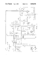
- FIG. 1 shows a schematic diagram of a crystal controlled amplitude modulated RF transmitter including a tripler stage.
- FIG. 2 shows a schematic diagram of an alternative RF transmitter including a fifth overtone crystal oscillator self-producing third harmonic.
- FIG. 3 shows a schematic diagram of an alternative RF transmitter including a frequency multiplying crystal oscillator of the type of FIG. 2 and a series resonant trap coupling the carrier frequency to the amplifier stage.
- FIG. 4 shows a front view of the improved antenna used in conjunction with the present invention.
- FIG. 5 shows a top view taken along reference lines 4--4 of FIG. 4.
- FIG. 1 a schematic diagram is shown of the present invention in relation to the integrated circuit sensor transmitter 2 of Applicant's U.S. Pat. No. 4,737,770 Because the circuitry and operation of the sensor transmitter 2 are discussed in detail in the co-pending application, they will not be discussed in any great detail herein.
- each sensor transmitter 2 comprises a programmable integrated circuit device which may be programmed with specific binary identification data descriptive of the security system and the particular transducer to which it is assigned. That is, along with identification data, each sensor transmitter 2 may be programmed with various preconditioning options peculiar to the specific transducer type to which it is coupled and relative to which the sensed inputs are processed to determine valid alarm (i.e. violation) and restore conditions. Upon the detection of either a violation or a restore signal, the sensor transmitter 2 produces a "data in" signal (i.e.
- the overall construction of the circuitry of FIG. 1 be as small as possible so that it is not detectable by an intruder.
- the sensor transmitter 2 and RF transmitter circuitry 8 are intended to be packaged into a container approximately 3 inches long and 1/2 inch in diameter. This size allows the package to be inserted into a drilled hole adjacent an associated magnet.
- somewhat larger, surface or recess mounted, packaging including a number of reed switches is contemplated.
- a program connector 14 which enables the system installer to physically couple a hand-held programming unit (not shown) to each of the sensor transmitters 2 as they are installed in relation to their associated transducer. Appropriate address and preconditioning data may thus be entered or changed at will.
- switches S1 and S2 are mounted at right angles to one another to two sides of the circuit board containing the sensor transmitter 2 and RF transmitter 8.
- Each switch along with an associated magnet, comprises one transducer which may be used for monitoring a door or window.
- This configuration is particularly advantageous in that it permits alternative mountings of the assembly and related magnet (not shown) in proximity to one of the switches S1 or S2 which, if interrupted, induces a change in switch state from open to closed and a violation transmission. Similarly, the re-opening of the affected switch causes a restore transmission.
- a tamper switch S3 coupled to the transmitter enclosure similarly induces a "tamper" transmission, if violated.
- the transmitter circuitry 8 of FIG. 1 is essentially comprised of three stages which are serially coupled to one another and are responsive to the "transmit enable" and "data in” signals on conductors 4 and 6 to transmit a corresponding amplitude modulated RF message to the CPU.
- these stages are a crystal oscillator stage 16, a tripler stage or multiplier 18 and an amplifier stage 20.
- the output of the transmitter 8, in turn, is coupled to the believed novel antenna which also couples power from a 3.6 volt battery source to the circuitry--the battery/antenna connection occurring at a battery clip integrally constructed as part of the antenna 10.
- the details of the antenna 10 will however be described hereinafter with respect to FIGS. 4 and 5.
- the three stages 16, 18 and 20, as with the other transmitter circuits of FIGS. 2 and 3, and the antenna 10 are designed to provide a maximum signal field strength at 319.5 MHz while attenuating all other undesired frequencies and harmonics, although the circuit of FIG. 3 best accomplishes these goals.
- the circuits are also designed to provide a parts count accommodating of the foregoing packaging size concerns in a cost effective design from the standpoint of discrete part cost and overall assembly costs.
- the crystal oscillator stage 16 generally comprises a fifth overtone producing, modified Pierce oscillator which oscillates at 106.5 MHz, although the crystal's K2 fundamental frequency is 21.3 MHz.
- tunable inductor L1 (21/2T) is set to promote resonance at the fifth overtone of the crystal's K2 fundamental frequency, while capacitor C6 (0.001 ⁇ f) serves as a bypass capacitor to the crystal's K2 fundamental frequency.
- Capacitor C8 (43 pf) is selected to provide the necessary phase shift for oscillation at the fifth overtone of the fundamental frequency (106.5 MHz) and to minimize a parasitic third harmonic of the fundamental frequency, while capacitors C7 (43 pf) and C14 (200 ⁇ f) couple the desired 106.5 MHz or fifth overtone output of the oscillator stage 16 to the tripler stage 18.
- the oscillator 16 requires a brief warmup period. Accordingly, the sensor transmitter 2, approximately 0.5 milliseconds before each message transmission, couples a transmit enable signal by way of conductor 6 to the oscillator 16 to induce oscillation.
- the sensor transmitter circuitry 2 couples its pulse position encoded data by way of conductor 4 and resistors R2 (100 k) and R3 (33 k) to the bases of transistors Q2 and Q3 (motorola mps-H10) of the respective tripler and amplifier stages 18 and 20.
- the 106.5 MHz frequency of the oscillator 16's output is converted and partially amplified to its third harmonic of 319.5 MHz.
- the resultant carrier signal is, in turn, amplified and amplitude modulated in correspondence with the pulse position encoded data at the amplifier stage 20 before it is transmitted by way of antenna 10.
- transistor Q2 of the tripler stage 18 is biased to operate in cutoff, since R2 is significantly larger than R3, to convert the 106.5 MHz input to the desired 319.5 MHz carrier frequency.
- Inductor L2 (11/2T) filters the resultant carrier of any undesired fundamental frequency component and capacitor C9 (100 pf) bypasses undesired frequencies to ground.
- Capacitor C10 (8.2 pf) and C11 (33 pf) in turn, attenuate unwanted frequencies other than the desired 319.5 MHz carrier frequency which is coupled to the amplifier output stage 20, wherein transistor Q3 is biased by resistor R3 (33 K) to operate in it linear range and modulate the carrier with the encoded security data. data.
- Inductor L3 (1.5 T) and capacitor C12 (7.5 pf) couple the modulated carrier to antenna 10 and capacitor C13 (2 pf) further attenuates unwanted frequencies.
- FIG. 1 an alternative embodiment of the transmitter circuitry of FIG. 1 is disclosed.
- This circuit principally differs from that of FIG. 1 in that it does not require a separate tripler stage 18.
- the crystal oscillator stage 16 is modified to not only oscillate at the crystal's fifth overtone frequency of 106.5 MHz but also to enhance the desired third harmonic carrier frequency of 319.5 MHz and at which frequency inductor L4 (1.5 T) and capacitors C7 (1 pf) and C14 (0.2 pf) resonate.
- the carrier frequency is, in turn, coupled by way of the tuned pi coupling network comprised of capacitors C14 (0.2 pf) and C16 (22 pf) and inductor L5 (4.5 T), to a two transistor amplifier output stage 20 including transistors Q2 and Q3 (NEC3544).
- the resultant 319.5 MHz carrier frequency is amplitude modulated with the encoded security data.
- the circuit of FIG. 2 adds inductor L4 (1.5 T) and capacitor C15 (150 pf) into transistor Q1's feedback path to obtain the necessary phase shift for fifth overtone oscillation at 106.5 MHz and to present a relatively high Q1 base impedance, without capacitor C8, at the desired third harmonic of the fifth overtone frequency or 319.5 MHz to enhance this otherwise parasitic harmonic.
- Inductor L1 (2.5 T) and capacitor C6 (220 pf) continue to reject any 21.3 MHz fundamental frequency component.
- the pi coupling network allows the extraction of the 319.5 MHz harmonic, without interfering with the oscillator's basic operation at 106.5 MHz.
- the pi coupling network also attenuates frequency components greater than the desired third harmonic carrier.
- FIG. 3 discloses yet another alternative, and presently preferred embodiment, of the transmitter circuitry 8. It generally operates in the same fashion as that of FIG. 2, except in lieu of a pi coupling network, a series resonant trap comprised of capacitor C17 (7.5 pf) and inductor L5 (4.5 T) is used to trap and couple the desired third harmonic carrier to a single transistor amplifier stage including transistor Q2(NEC 3544).
- This circuit has also been found to meet the pertinent regulatory requirements, while also providing a reduced 25 parts count to better meet the previously mentioned packaging and cost goals.
- the 319.5 MHz carrier frequency is appropriately modulated, it is coupled to the antenna 10 which, from an operational standpoint, need merely comprise a sufficiently long conductor having enough surface area to ensure reasonably noise-free transmissions over the relative short, intended transmission distances of one thousand feet. Consequently, a bare wire may suffice.
- the present invention further contemplates fabricating the required clip connector as part of the antenna.
- the antenna is thus constructed, for example, from beryllium or other suitably conductive/flexive materials.
- the antenna 10 of FIGS. 5 2 and 3 is constructed from flat stock beryllium.
- a solid conductor might be used with less cost, but which would also require a separate battery clip.
- FIGS. 4 and 5 wherein a front view of the antenna is shown in FIG. 4 and a top view, taken along reference lines 5--5 of FIG. 4, is shown in FIG. 5.
- the one end of the antenna is constructed with a vertically disposed, inverted U-shaped portion that is brought into spring contact with the positive end of the 3.6 volt battery power supply.
- a battery holder or separate battery clips are not required and which, as mentioned, facilitates the reduction of overall package size and cost.
- the battery is mounted in parallel relation to the horizontal portion 10a of the antenna 10.
- the circuitry of FIG. 1 is mounted within the interior C-shaped area of the antenna 10, with the programming terminal 14 being mounted at the lower right open corner.
- Formed pin connectors 24 are also provided for solder mounting the antenna 10 to a printed circuit board (not shown).
- a further advantage of the above surrounding construction is that the antenna 10 also acts to physically protect the circuit components from damage such as might typically be encountered at the installation site and/or during inventorying.
Landscapes
- Engineering & Computer Science (AREA)
- Computer Networks & Wireless Communication (AREA)
- Signal Processing (AREA)
- Transmitters (AREA)
Abstract
Description
Claims (7)
Priority Applications (1)
| Application Number | Priority Date | Filing Date | Title |
|---|---|---|---|
| US07/016,561 US4864636A (en) | 1987-02-19 | 1987-02-19 | Crystal controlled transmitter |
Applications Claiming Priority (1)
| Application Number | Priority Date | Filing Date | Title |
|---|---|---|---|
| US07/016,561 US4864636A (en) | 1987-02-19 | 1987-02-19 | Crystal controlled transmitter |
Publications (1)
| Publication Number | Publication Date |
|---|---|
| US4864636A true US4864636A (en) | 1989-09-05 |
Family
ID=21777765
Family Applications (1)
| Application Number | Title | Priority Date | Filing Date |
|---|---|---|---|
| US07/016,561 Expired - Lifetime US4864636A (en) | 1987-02-19 | 1987-02-19 | Crystal controlled transmitter |
Country Status (1)
| Country | Link |
|---|---|
| US (1) | US4864636A (en) |
Cited By (21)
| Publication number | Priority date | Publication date | Assignee | Title |
|---|---|---|---|---|
| WO1991009317A2 (en) * | 1989-12-11 | 1991-06-27 | Österreichisches Forschungszentrum Seibersdorf Ges.M.B.H. | Comb generator, device and process for calibrating measurement sections |
| US5079559A (en) * | 1988-10-26 | 1992-01-07 | Nec Corporation | Dual plate antenna |
| WO1993004540A1 (en) * | 1991-08-21 | 1993-03-04 | L.S. Research, Inc. | System for short-range transmission of signals over the air using a high frequency carrier |
| US5214568A (en) * | 1989-08-07 | 1993-05-25 | Heng Fook K | Transmission system |
| US5223801A (en) * | 1992-03-30 | 1993-06-29 | Interactive Technologies, Inc. | Crystal oscillator and transmitter operating at the third harmonic of the fifth overtone of a crystal |
| US5227805A (en) * | 1989-10-26 | 1993-07-13 | Motorola, Inc. | Antenna loop/battery spring |
| US5227804A (en) * | 1988-07-05 | 1993-07-13 | Nec Corporation | Antenna structure used in portable radio device |
| EP0552598A2 (en) * | 1992-01-21 | 1993-07-28 | NPBI Nederlands Produktielaboratorium voor Bloedtransfusieapparatuur en Infusievloeistoffen B.V. | Apparatus for sealing medical plastic tubing |
| US5301361A (en) * | 1990-12-28 | 1994-04-05 | Samson Technologies | Low parts count transmitter unit |
| US5491839A (en) * | 1991-08-21 | 1996-02-13 | L. S. Research, Inc. | System for short range transmission of a plurality of signals simultaneously over the air using high frequency carriers |
| US5673323A (en) * | 1995-04-12 | 1997-09-30 | L. S. Research, Inc. | Analog spread spectrum wireless speaker system |
| US6058294A (en) * | 1998-03-24 | 2000-05-02 | Microchip Technology Incorporated | Adjustable frequency stabilizing internal chip capacitor system |
| US6515458B1 (en) * | 2001-04-26 | 2003-02-04 | Ion Systems, Inc. | Pulse oscillator and voltage level converter |
| US6737969B2 (en) | 2001-11-27 | 2004-05-18 | Ion Digital Llp | Wireless security sensor systems for windows and doors |
| US20050024207A1 (en) * | 2003-06-06 | 2005-02-03 | Schebel Dean David | Compact wireless sensor |
| US20050122177A1 (en) * | 2003-12-08 | 2005-06-09 | Alps Electric Co., Ltd. | Voltage controlled oscillator for frequency synthesizer |
| US20050229654A1 (en) * | 2003-12-16 | 2005-10-20 | Hugh Victor | Securing system and method |
| US20070085668A1 (en) * | 2005-10-13 | 2007-04-19 | Pacific Industrial Co., Ltd. | Tire condition monitoring device |
| US20080034635A1 (en) * | 2006-08-11 | 2008-02-14 | Hugh Victor | Securing system with housing for hardware |
| WO2014029413A1 (en) * | 2012-08-20 | 2014-02-27 | Telefonaktiebolaget L M Ericsson (Publ) | Device for frequency tripling |
| WO2015081983A1 (en) * | 2013-12-02 | 2015-06-11 | Telefonaktiebolaget L M Ericsson (Publ) | A sub-harmonic mixer and a method therein for converting radio frequency signals to intermediate frequency signals |
Citations (8)
| Publication number | Priority date | Publication date | Assignee | Title |
|---|---|---|---|---|
| US2884526A (en) * | 1957-12-02 | 1959-04-28 | Vincent J Cortese | Oscillator output circuit |
| US3108223A (en) * | 1961-10-23 | 1963-10-22 | Harry E Aine | Miniature radio beacon apparatus |
| US3311812A (en) * | 1967-03-28 | Broadband solid state microwave energy source | ||
| US3742496A (en) * | 1971-01-07 | 1973-06-26 | Itt | Precision dme compatible with tacan |
| US4384288A (en) * | 1980-12-31 | 1983-05-17 | Walton Charles A | Portable radio frequency emitting identifier |
| US4591863A (en) * | 1984-04-04 | 1986-05-27 | Motorola, Inc. | Low profile antenna suitable for use with two-way portable transceivers |
| US4635296A (en) * | 1985-02-22 | 1987-01-06 | Transkinetic Systems, Inc. | Wide bandwidth ultra high stability FM telemetry transmitter |
| US4641366A (en) * | 1984-10-04 | 1987-02-03 | Nec Corporation | Portable radio communication apparatus comprising an antenna member for a broad-band signal |
-
1987
- 1987-02-19 US US07/016,561 patent/US4864636A/en not_active Expired - Lifetime
Patent Citations (8)
| Publication number | Priority date | Publication date | Assignee | Title |
|---|---|---|---|---|
| US3311812A (en) * | 1967-03-28 | Broadband solid state microwave energy source | ||
| US2884526A (en) * | 1957-12-02 | 1959-04-28 | Vincent J Cortese | Oscillator output circuit |
| US3108223A (en) * | 1961-10-23 | 1963-10-22 | Harry E Aine | Miniature radio beacon apparatus |
| US3742496A (en) * | 1971-01-07 | 1973-06-26 | Itt | Precision dme compatible with tacan |
| US4384288A (en) * | 1980-12-31 | 1983-05-17 | Walton Charles A | Portable radio frequency emitting identifier |
| US4591863A (en) * | 1984-04-04 | 1986-05-27 | Motorola, Inc. | Low profile antenna suitable for use with two-way portable transceivers |
| US4641366A (en) * | 1984-10-04 | 1987-02-03 | Nec Corporation | Portable radio communication apparatus comprising an antenna member for a broad-band signal |
| US4635296A (en) * | 1985-02-22 | 1987-01-06 | Transkinetic Systems, Inc. | Wide bandwidth ultra high stability FM telemetry transmitter |
Cited By (37)
| Publication number | Priority date | Publication date | Assignee | Title |
|---|---|---|---|---|
| US5227804A (en) * | 1988-07-05 | 1993-07-13 | Nec Corporation | Antenna structure used in portable radio device |
| US5079559A (en) * | 1988-10-26 | 1992-01-07 | Nec Corporation | Dual plate antenna |
| US5214568A (en) * | 1989-08-07 | 1993-05-25 | Heng Fook K | Transmission system |
| US5227805A (en) * | 1989-10-26 | 1993-07-13 | Motorola, Inc. | Antenna loop/battery spring |
| WO1991009317A3 (en) * | 1989-12-11 | 1991-09-19 | Oesterr Forsch Seibersdorf | Comb generator, device and process for calibrating measurement sections |
| US5594458A (en) * | 1989-12-11 | 1997-01-14 | Oesterreichisches Forschungszentrum Seibersdorf Ges.M.B.H. | Comb generator, device and process for calibrating measurement sections |
| WO1991009317A2 (en) * | 1989-12-11 | 1991-06-27 | Österreichisches Forschungszentrum Seibersdorf Ges.M.B.H. | Comb generator, device and process for calibrating measurement sections |
| US5301361A (en) * | 1990-12-28 | 1994-04-05 | Samson Technologies | Low parts count transmitter unit |
| US5491839A (en) * | 1991-08-21 | 1996-02-13 | L. S. Research, Inc. | System for short range transmission of a plurality of signals simultaneously over the air using high frequency carriers |
| US5299264A (en) * | 1991-08-21 | 1994-03-29 | L. S. Research, Inc. | System for short-range transmission of signals over the air using a high frequency carrier |
| US5581617A (en) * | 1991-08-21 | 1996-12-03 | L. S. Research, Inc. | System for short-range transmission of signals over the air using a high frequency carrier |
| WO1993004540A1 (en) * | 1991-08-21 | 1993-03-04 | L.S. Research, Inc. | System for short-range transmission of signals over the air using a high frequency carrier |
| EP0552598A3 (en) * | 1992-01-21 | 1993-09-08 | Npbi Nederlands Produktielaboratorium Voor Bloedtransfusieapparatuur En Infusievloeistoffen B.V. | Apparatus for sealing medical plastic tubing |
| EP0552598A2 (en) * | 1992-01-21 | 1993-07-28 | NPBI Nederlands Produktielaboratorium voor Bloedtransfusieapparatuur en Infusievloeistoffen B.V. | Apparatus for sealing medical plastic tubing |
| US5223801A (en) * | 1992-03-30 | 1993-06-29 | Interactive Technologies, Inc. | Crystal oscillator and transmitter operating at the third harmonic of the fifth overtone of a crystal |
| US5673323A (en) * | 1995-04-12 | 1997-09-30 | L. S. Research, Inc. | Analog spread spectrum wireless speaker system |
| US6058294A (en) * | 1998-03-24 | 2000-05-02 | Microchip Technology Incorporated | Adjustable frequency stabilizing internal chip capacitor system |
| US6515458B1 (en) * | 2001-04-26 | 2003-02-04 | Ion Systems, Inc. | Pulse oscillator and voltage level converter |
| US6737969B2 (en) | 2001-11-27 | 2004-05-18 | Ion Digital Llp | Wireless security sensor systems for windows and doors |
| US20050024207A1 (en) * | 2003-06-06 | 2005-02-03 | Schebel Dean David | Compact wireless sensor |
| US7081816B2 (en) | 2003-06-06 | 2006-07-25 | Ion Digital Llp | Compact wireless sensor |
| US7292108B2 (en) | 2003-12-08 | 2007-11-06 | Alps Electric Co., Ltd. | Voltage controlled oscillator for frequency synthesizer |
| US20050122177A1 (en) * | 2003-12-08 | 2005-06-09 | Alps Electric Co., Ltd. | Voltage controlled oscillator for frequency synthesizer |
| EP1542355A1 (en) * | 2003-12-08 | 2005-06-15 | Alps Electric Co., Ltd. | Voltage controlled oscillator for frequency synthesizer |
| US20100218567A1 (en) * | 2003-12-16 | 2010-09-02 | Hugh Victor | Securing system and method |
| US7281397B2 (en) | 2003-12-16 | 2007-10-16 | Hugh Victor | Securing system and method |
| US20080245117A1 (en) * | 2003-12-16 | 2008-10-09 | Hugh Victor | Securing system and method |
| US7730750B2 (en) | 2003-12-16 | 2010-06-08 | Hugh Victor | Securing system and method |
| US20050229654A1 (en) * | 2003-12-16 | 2005-10-20 | Hugh Victor | Securing system and method |
| US8402799B2 (en) | 2003-12-16 | 2013-03-26 | Hugh Victor | Securing system and method |
| US20070085668A1 (en) * | 2005-10-13 | 2007-04-19 | Pacific Industrial Co., Ltd. | Tire condition monitoring device |
| US20080034635A1 (en) * | 2006-08-11 | 2008-02-14 | Hugh Victor | Securing system with housing for hardware |
| US7584566B2 (en) | 2006-08-11 | 2009-09-08 | Hugh Victor | Securing system with housing for hardware |
| US8186088B2 (en) | 2006-08-11 | 2012-05-29 | Hugh Victor | Securing system with housing for hardware |
| WO2014029413A1 (en) * | 2012-08-20 | 2014-02-27 | Telefonaktiebolaget L M Ericsson (Publ) | Device for frequency tripling |
| WO2015081983A1 (en) * | 2013-12-02 | 2015-06-11 | Telefonaktiebolaget L M Ericsson (Publ) | A sub-harmonic mixer and a method therein for converting radio frequency signals to intermediate frequency signals |
| US9912293B2 (en) | 2013-12-02 | 2018-03-06 | Telefonaktiebolaget Lm Ericsson (Publ) | Sub-harmonic mixer and a method therein for converting radio frequency signals to intermediate frequency signals |
Similar Documents
| Publication | Publication Date | Title |
|---|---|---|
| US4864636A (en) | Crystal controlled transmitter | |
| US4794622A (en) | Low power transmitter frequency stabilization | |
| US6130612A (en) | Antenna for RF tag with a magnetoelastic resonant core | |
| US5920234A (en) | Buffered oscillator transmitter arrangement for power specific applications having parasitic impedances | |
| KR920701919A (en) | Proximity detector | |
| CA2284600A1 (en) | Apparatus for magnetically decoupling an rfid tag | |
| US5257033A (en) | Transmitter with a reduction of power of signals transmitted at harmonics | |
| EP0793874B1 (en) | An oscillator and transmitter arrangement | |
| CA1279899C (en) | Security system with saw transmitter | |
| EP0486087A2 (en) | Apparatus for receiving and transmitting RF signals | |
| US5223801A (en) | Crystal oscillator and transmitter operating at the third harmonic of the fifth overtone of a crystal | |
| US6373469B1 (en) | Radio frequency computer mouse | |
| US4531115A (en) | Remote alarm system | |
| EP0648009B1 (en) | Oscillating circuit | |
| US4485382A (en) | Tuning circuits with bendable U-shaped variable inductor for garage door actuators | |
| US5486793A (en) | Balanced RF oscillator and transmitter | |
| JPS61116425A (en) | High-frequency electromagnetic wave signal transmission system | |
| US6232846B1 (en) | Oscillator module and communications device using the same | |
| JPS61149880A (en) | Frequency sensor | |
| EP1154559B1 (en) | Oscillator | |
| US3898582A (en) | Transmitter encoder with output for a time period | |
| EP0767540A2 (en) | Radio transmitter | |
| US6369664B1 (en) | Voltage controlled oscillator and electronic apparatus using same | |
| US5668981A (en) | Apparatus having radiating noise damping means for controlling power appliances | |
| EP1111769A2 (en) | Oscillator |
Legal Events
| Date | Code | Title | Description |
|---|---|---|---|
| AS | Assignment |
Owner name: INTERACTIVE TECHNOLOGIES, INC., 2266 N. SECOND ST. Free format text: ASSIGNMENT OF ASSIGNORS INTEREST.;ASSIGNOR:BRUNIUS, ROBERT E.;REEL/FRAME:004681/0150 Effective date: 19870128 |
|
| STCF | Information on status: patent grant |
Free format text: PATENTED CASE |
|
| AS | Assignment |
Owner name: NORWEST BANK MINNESOTA, NATIONAL ASSOCIATION, AS A Free format text: SECURITY INTEREST;ASSIGNOR:INTERACTIVE TECHNOLOGIES, INC.;REEL/FRAME:006122/0071 Effective date: 19920511 |
|
| AS | Assignment |
Owner name: INTERACTIVE TECHNOLOGIES, INC., A MN CORP., MINNES Free format text: ASSIGNMENT OF ASSIGNORS INTEREST.;ASSIGNOR:BRUNIUS, ROBERT E.;REEL/FRAME:006109/0800 Effective date: 19920511 |
|
| FPAY | Fee payment |
Year of fee payment: 4 |
|
| FEPP | Fee payment procedure |
Free format text: PAT HLDR NO LONGER CLAIMS SMALL ENT STAT AS INDIV INVENTOR (ORIGINAL EVENT CODE: LSM1); ENTITY STATUS OF PATENT OWNER: LARGE ENTITY |
|
| REMI | Maintenance fee reminder mailed | ||
| FPAY | Fee payment |
Year of fee payment: 8 |
|
| SULP | Surcharge for late payment | ||
| FPAY | Fee payment |
Year of fee payment: 12 |