US4871224A - Device for optical connections of one or more optical emitters with one or more optical detectors of one or more integrated circuits - Google Patents
Device for optical connections of one or more optical emitters with one or more optical detectors of one or more integrated circuits Download PDFInfo
- Publication number
- US4871224A US4871224A US07/322,410 US32241089A US4871224A US 4871224 A US4871224 A US 4871224A US 32241089 A US32241089 A US 32241089A US 4871224 A US4871224 A US 4871224A
- Authority
- US
- United States
- Prior art keywords
- optical
- spacer
- light
- waveguide
- cover member
- Prior art date
- Legal status (The legal status is an assumption and is not a legal conclusion. Google has not performed a legal analysis and makes no representation as to the accuracy of the status listed.)
- Expired - Fee Related
Links
Images


Classifications
-
- G—PHYSICS
- G02—OPTICS
- G02B—OPTICAL ELEMENTS, SYSTEMS OR APPARATUS
- G02B6/00—Light guides; Structural details of arrangements comprising light guides and other optical elements, e.g. couplings
- G02B6/24—Coupling light guides
- G02B6/42—Coupling light guides with opto-electronic elements
- G02B6/43—Arrangements comprising a plurality of opto-electronic elements and associated optical interconnections
-
- H—ELECTRICITY
- H04—ELECTRIC COMMUNICATION TECHNIQUE
- H04B—TRANSMISSION
- H04B10/00—Transmission systems employing electromagnetic waves other than radio-waves, e.g. infrared, visible or ultraviolet light, or employing corpuscular radiation, e.g. quantum communication
- H04B10/80—Optical aspects relating to the use of optical transmission for specific applications, not provided for in groups H04B10/03 - H04B10/70, e.g. optical power feeding or optical transmission through water
- H04B10/801—Optical aspects relating to the use of optical transmission for specific applications, not provided for in groups H04B10/03 - H04B10/70, e.g. optical power feeding or optical transmission through water using optical interconnects, e.g. light coupled isolators, circuit board interconnections
-
- H—ELECTRICITY
- H01—ELECTRIC ELEMENTS
- H01L—SEMICONDUCTOR DEVICES NOT COVERED BY CLASS H10
- H01L2224/00—Indexing scheme for arrangements for connecting or disconnecting semiconductor or solid-state bodies and methods related thereto as covered by H01L24/00
- H01L2224/01—Means for bonding being attached to, or being formed on, the surface to be connected, e.g. chip-to-package, die-attach, "first-level" interconnects; Manufacturing methods related thereto
- H01L2224/42—Wire connectors; Manufacturing methods related thereto
- H01L2224/47—Structure, shape, material or disposition of the wire connectors after the connecting process
- H01L2224/48—Structure, shape, material or disposition of the wire connectors after the connecting process of an individual wire connector
- H01L2224/4805—Shape
- H01L2224/4809—Loop shape
- H01L2224/48091—Arched
-
- H—ELECTRICITY
- H01—ELECTRIC ELEMENTS
- H01L—SEMICONDUCTOR DEVICES NOT COVERED BY CLASS H10
- H01L2224/00—Indexing scheme for arrangements for connecting or disconnecting semiconductor or solid-state bodies and methods related thereto as covered by H01L24/00
- H01L2224/01—Means for bonding being attached to, or being formed on, the surface to be connected, e.g. chip-to-package, die-attach, "first-level" interconnects; Manufacturing methods related thereto
- H01L2224/42—Wire connectors; Manufacturing methods related thereto
- H01L2224/47—Structure, shape, material or disposition of the wire connectors after the connecting process
- H01L2224/48—Structure, shape, material or disposition of the wire connectors after the connecting process of an individual wire connector
- H01L2224/481—Disposition
- H01L2224/48135—Connecting between different semiconductor or solid-state bodies, i.e. chip-to-chip
- H01L2224/48137—Connecting between different semiconductor or solid-state bodies, i.e. chip-to-chip the bodies being arranged next to each other, e.g. on a common substrate
Definitions
- the present invention is directed to a device for the optical connection of one or more optical emitters with one or more optical detectors of one or more integrated circuits.
- a device for the optical connection of a plurality of optical emitters that are allocated to a common, integrated circuit and have a plurality of optical detectors of this circuit is known and disclosed in an article from App. Optics, Vol. 26, No. 20, Oct. 15, 1987, pp. 4377-4384.
- an optical installation for directing of the light emitted by an optical emitter to several optical detectors is composed of a hologram which is arranged above the emitter and the integrated circuit.
- the hologram is supplied with light emitted by an emitter and will distribute this supplied light to certain optical detectors on the integrated circuit.
- a device for the optical connection of several optical emitters with several optical detectors is known from an article in App. Optics, Vol. 26, No. 17, Sept. 1, 1987, pp. 3649-3654.
- the optical emitters are arranged on a substrate and are covered by a transparent, layered alignment template.
- a Fresnel phase plate lens is arranged as an optical device for the directing of the light emitted by an optical emitter to one or several optical detectors.
- This phase plate lens directs the light, which is emitted by the optical emitters and permeates both a template and the layer of silicon, to the optical detectors, which are arranged on the layer of silicon on the side of the layer which is facing away from the lens and emitters.
- the object of the present invention is to create a device for the optical connection of one or more optical emitters with one or more optical detectors of one or more integrated circuits, which device requires an optimally small constructional cost and has a high precision for manufacturing external optical connections of various integrated circuits, particularly of computer chips, as well as internal optical connections in the case of individual integrated circuits, as well as such external and internal optical connections and combinations.
- the present invention is directed to a device for the connection of an optical emitter with an optical detector of an integrated circuit, said device having a common substrate, each integrated circuit, an optical emitter and optical detector being in the form of components and being secured on said substrate, a spacer being secured on said substrate and having a first surface extending away from said substrate, a cover having a second surface and being mounted on the spacer with the second surface of the cover facing the first surface of the spacer, and optical means for guiding light emitted by an optical emitter to an optical detector being attached to one of said first and second surfaces.
- This solution makes it possible to manufacture in a simple manner and with high precision, internal and external optical connections in or between integrated semiconductor chips with basically only three components.
- a particular advantage is that the external and internal optical connections can be manufactured in combination with each other.
- the substrate, the spacer and cover member of the same material or of materials which have basically the same thermal expansion coefficient.
- this material is anisotropically etchable and, thus, enables a simple manufacturing of oblique side faces which are required in certain embodiments of the invention.
- An expedient embodiment of the spacer of the device according to the invention which can be manufactured in a simple manner and with a high accuracy with a standard lithographic method and can, furthermore, be universally employed, is by forming the spacer of one or more layers to overlap each other and have one or several recess regions existing to proceed across the entire thickness of the layer in which the various components, which are to be secured to the substrate, can be arranged.
- An embodiment of the invention has the optical means constructed as a waveguide structure, which is arranged either on the first surface of the spacer or between the first surface and the second surface.
- the waveguide receives the light emitted by the emitter and couples this out to the desired detectors. This is advantageous for manufacturing external optical connections between various optical circuits, for example between computer chips, in order to enable a data exchange between these chips.
- the waveguide structure can be one or more strip waveguides which may be, preferably, of glass. This is desirable, since the structure can be etched out of an easily producible glass layer in a very simple manner with the assistance of standard lithographic processes.
- the coupling of optical emitters and optical detectors to the waveguide structure can be performed in different ways. These ways include either arranging the output of the emitter directly opposite an end face of the waveguide or concentrating the light from the emitter with a lens and deflecting the light by two deflection elements onto the end face of the waveguide.
- the optical detectors can be coupled to the ends of the waveguide either by having a detector window arranged opposite to the end face of the waveguide or by having the light exiting the waveguide being deflected by a deflecting element onto the detector of the waveguide.
- the cover member is provided with a recess which can consist of a window-like opening so that parts of the particular component can extend above the plane of the waveguide.
- the optical means supplies light emitted by at least one of the optical emitters to optical detectors that are allocated in various components with integrated circuits.
- the spacers are provided for a recess region for each of the components.
- the optical means is a light distribution element which is either fashioned or attached on a bottom surface of the cover member and this light distribution element is supplied by a light emitted by an optical emitter that is allocated to a certain component with an integrated circuit and distributes the light to optical detectors that are allocated to this certain component.
- the optical means is a light distribution element which is either fashioned or attached on a bottom surface of the cover member and this light distribution element is supplied by a light emitted by an optical emitter that is allocated to a certain component with an integrated circuit and distributes the light to optical detectors that are allocated to this certain component.
- the optical means is arranged on the first surface for the guidance of light emitted by the optical emitter arranged in the recess region of the spacer to an optical detector arranged in another recess region in the spacer and that the optical means includes light distributing elements which are attached in the cover plate at each recess for distributing light from the emitter of that particular recess to detectors located in that recess.
- FIG. 1 is a cross sectional view of an embodiment of the device wherein two silicon chips with integrated circuits are externally connected with each other by an optical parallel connection;
- FIG. 2 is a cross sectional view of a different embodiment of a device similar to the device of FIG. 1;
- FIG. 3 is an enlarged partial cross sectional view of an embodiment of the device wherein the optical emitter that is allocated to a silicon chip with an integrated circuit is optimally connected with detectors of this chip so that internal optical connection is provided;
- FIG. 4 is a cross sectional view through an embodiment of the device wherein silicon chips with integrated circuits are externally, optically connected and whereby each chip is internally, optically connected as well;
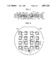
- FIG. 5 is a plan view with portions removed for purposes of illustration of the arrangement of FIG. 4.
- the principles of the present invention are particularly useful when incorporated in a device, such as illustrated in FIG. 1.
- the device of FIG. 1 includes a substrate Su, a spacer Ah and a cover member DK, which are all composed of a layer of silicon, whose thickness is in the range of 300 ⁇ m-1000 ⁇ m.
- the spacer Ah is mounted on the substrate Su and, on the left end, there is a silicon chip with an integrated circuit IC, which is secured on the substrate Su.
- This chip includes an optical emitter oS, which is in the form of a laser diode or array which proceeds along a line extending perpendicular to the plane of the drawing. This optical emitter oS is allocated to the integrated circuit IC.
- an optical detector oD in the form of a photodetector or array that extends along the line which is perpendicular to the plane of the drawing is mounted on the substrate, and this optical detector oD is allocated to an integrated circuit IC2 arranged on this one side.
- the optical emitter oS is electrically connected with the allocated integrated circuit IC and is controlled by this circuit, whereas the optical detector oD is electrically connected to the integrate circuit IC2, which is allocated to it and which controls it.
- the optical emitter oS and the optical oD are components that are separated from the semiconductor chip; however, they could also be integrated on the chip, as in the case of the optical detector oD on the chip IC3 of FIG. 3.
- the spacer Ah is a layer with a recess region Be in which the components are fastened on the substrate Su.
- they can be fastened by gluing.
- These regions Be can be simply produced by etching.
- the spacer Ah is covered by a cover member DK. Between the cover member DK and the spacer Ah is optical means for guiding light, which is illustrated in the embodiment of FIG. 1 as a waveguide structure Wst.
- the waveguide structure is composed of parallel strip waveguides which are, preferably, composed of glass. Each strip extends from a laser diode of the optical emitter oS to the allocated photodetector of the optical detector oD.
- This waveguide structure Wst can be produced in a simple manner in that a glass layer, for example a thickness in the range of 8 ⁇ m-50 ⁇ m, is applied on the spacer Ah or onto a cover member DK and in that the desired waveguide structure Wst is etched out of this layer with the assistance of a standard photolithographic process.
- the glass layer can be attached, for example with the assistance of a known CVD-method.
- the optical emitter oS emits light in the plane of the strip waveguide structure Wst.
- the light emitting area eB of this emitter oS lies opposite an end face Stf of the waveguide of the strip waveguide structure through which the light emitted by the emitter oS is coupled into the waveguide structure Wst.
- a base Sm can be used, which is dimensioned appropriately and fastened on the emitter oS.
- a recess Asp is provided in the cover DK in that area of the optical emitter into which these parts T are arranged.
- This recess Asp can be fashioned, for example, in the form of a window in the cover member DK and can be produced by etching, for example by preferential etching of silicon.
- the recess Asp can also be provided at different locations in the cover member DK, for example, at each location at which components with integrated circuits are fastened on the substrate Su.
- outcoupling to the optical detector oD occurs via a deflection element Ue3.
- This deflection element Ue3 deflects or reflects the light outcoupled at the end face Stf of the waveguide structure Wst to a detector window Df which faces the cover member DK.
- This deflecting element Ue3 can be composed, for example, of an oblique end face of a short waveguide section Wa, which is fastened on a bottom or second surface of the cover member DK so that the light being coupled out of the waveguide structure Wst falls onto the oblique end face.
- the optical detector oD could also be arranged so that its detector window Df lies opposite the end face Stf of a waveguide of the waveguide structure Wst. The light outcoupled by this end face would be directly guided to the detector window Df. In this case, the recess Asp provided on the detector side in the embodiment according to FIG. 1 would be necessary.
- the thickness of the spacer Ah can be bigger than the maximum height of the component fastened on the substrate, such as by gluing. Then recesses in the cover member DK would not be necessary in this arrangement.
- FIG. 2 shows an embodiment wherein the in- and outcoupling occur by deflection.
- This embodiment according to FIG. 2 differs from the embodiment of FIG. 1 merely in that the incoupling of the light and the waveguide structure Wst occurs via deflection and that no recesses are provided in the cover member DK.
- the light emitted by the optical emitter oS in a parallel fashion to the plane of the waveguide structure Wst diverges.
- This light is concentrated on one end face Stf of a waveguide of the waveguide structure Wst by a focussing and collecting lens Li and by two deflecting elements Ue1 and Ue2.
- the lens Li which is mounted on a base (not illustrated) is fastened on a substrate Su and can be a glass bar which is arranged to extend along a line extending perpendicular to the plane of the drawing.
- the first deflecting element Ue1 expediently consists of an oblique side face of the spacer Ah and deflects or reflects the light in a direction to a second or other deflecting element Ue2.
- the oblique side face can be produced by anisotropic etching of the silicon layer forming the spacer Ah.
- the other deflecting element Ue2 is formed by an oblique end face of a short waveguide section Wa, which is fastened on the bottom or second surface of the cover member DK such that the oblique end face Ue2 deflects the light striking it into the end face Stf of the waveguide of the waveguide structure Wst.
- the spacer Ah is formed or composed of two silicon layers Sch1 and Sch2.
- the bottom silicon layer Sch1 has an oblique side face forming a deflection element Ue which can be produced by anisotropic etching.
- the light emitted by the optical emitter oS which may be a laser diode, in the direction of the deflecting element Ue is deflected or reflected by this element Ue to a light distribution element Ho1, which is attached or constructed on a second surface of the cover member DK and distributes the light supplied to it to optical detectors oD, which are integrated on a semiconductor chip with an integrated circuit IC3 and these detectors are formed as photodetectors.
- the light distribution element can be a hologram, for example.
- the embodiment according to FIG. 3 has the advantage that it is compatible with the embodiments of FIGS. 1 and 2.
- a device illustrated in FIGS. 4 and 5 shows an embodiment wherein the optical connection illustrated in FIGS. 1 and 2, as well as the optical connection according to the embodiment of FIG. 3, are realized and provided on the same substrate Su.
- the substrate Su is composed of a silicon wafer on which a first layer Sch1 of a spacer Ah is fastened and this layer Sch1 has a plurality of rectangular recess regions Be. In each rectangular recess region Be, a semiconductor chip with an integrated circuit IC and an optical emitter oS is arranged.
- a strip waveguide structure Wst is fashioned as well. The waveguide of this structure directs light emitted by an optical emitter oS of a clock generator TG (FIG. 5) to optical detectors oD of the various integrated circuits IC.
- the side faces of the recess regions Be of the first layer Sch1 are oblique so that they can constitute deflecting elements Ue.
- a second layer Sch2 of the spacer Ah is applied and has recess regions Be that correspond to the recess regions Be of the first layer Sch1.
- the cover member DK is applied.
- a light distributing element Ho1 is attached on the bottom or second surface of the cover member DK so that an optical connection according to FIG. 3 is obtained in each of these regions.
- the recess regions Be can be produced with a high degree of accuracy by etching or by anisotropic etching of silicon wafers. Since the same material is used for all of the layers, no thermal tensions or stresses will occur.
- the fastening of the substrate Su, the spacer Ah and the cover DK relative to one another can occur, for example by glue or by threaded or screw connections.
Abstract
A device for optically connecting one or several optical emitters with one or several optical detectors of integrated circuits characterized by a substrate, a spacer disposed on the substrate providing recesses for each of the integrated circuits and components and a cover plate with either a light waveguide structure extending between the various emitters and detectors interposed either between the cover plate and spacer or on one of the cover plates and spacers or a distributing element positioned on a surface of the cover plate for distributing light emitted by the optical emitter in one recess to the detectors of the same recess or both. The waveguide system allows interconnecting an optical emitter of one unit or component with a detector of another unit component or components. The distributing element allows connecting the optical emitter to the optical detector of a single unit. Thus, selection of the two types of optical arrangements allows an external connection of one component to another component or internal connections of elements of a single component.
Description
The present invention is directed to a device for the optical connection of one or more optical emitters with one or more optical detectors of one or more integrated circuits.
A device for the optical connection of a plurality of optical emitters that are allocated to a common, integrated circuit and have a plurality of optical detectors of this circuit is known and disclosed in an article from App. Optics, Vol. 26, No. 20, Oct. 15, 1987, pp. 4377-4384. As disclosed, an optical installation for directing of the light emitted by an optical emitter to several optical detectors is composed of a hologram which is arranged above the emitter and the integrated circuit. The hologram is supplied with light emitted by an emitter and will distribute this supplied light to certain optical detectors on the integrated circuit. This publication contains no detailed information how the detectors, the hologram and the integrated circuits are fastened relative to one another.
A device for the optical connection of several optical emitters with several optical detectors is known from an article in App. Optics, Vol. 26, No. 17, Sept. 1, 1987, pp. 3649-3654. As disclosed, the optical emitters are arranged on a substrate and are covered by a transparent, layered alignment template. Between this template and a layer of silicon, a Fresnel phase plate lens is arranged as an optical device for the directing of the light emitted by an optical emitter to one or several optical detectors. This phase plate lens directs the light, which is emitted by the optical emitters and permeates both a template and the layer of silicon, to the optical detectors, which are arranged on the layer of silicon on the side of the layer which is facing away from the lens and emitters.
The object of the present invention is to create a device for the optical connection of one or more optical emitters with one or more optical detectors of one or more integrated circuits, which device requires an optimally small constructional cost and has a high precision for manufacturing external optical connections of various integrated circuits, particularly of computer chips, as well as internal optical connections in the case of individual integrated circuits, as well as such external and internal optical connections and combinations.
To accomplish these goals, the present invention is directed to a device for the connection of an optical emitter with an optical detector of an integrated circuit, said device having a common substrate, each integrated circuit, an optical emitter and optical detector being in the form of components and being secured on said substrate, a spacer being secured on said substrate and having a first surface extending away from said substrate, a cover having a second surface and being mounted on the spacer with the second surface of the cover facing the first surface of the spacer, and optical means for guiding light emitted by an optical emitter to an optical detector being attached to one of said first and second surfaces. This solution makes it possible to manufacture in a simple manner and with high precision, internal and external optical connections in or between integrated semiconductor chips with basically only three components. A particular advantage is that the external and internal optical connections can be manufactured in combination with each other.
In order for the achievement of high precision and to remain durable, it is expedient to create the substrate, the spacer and cover member of the same material or of materials which have basically the same thermal expansion coefficient. Thus, it is expedient to form these as silicon because this material is anisotropically etchable and, thus, enables a simple manufacturing of oblique side faces which are required in certain embodiments of the invention.
An expedient embodiment of the spacer of the device according to the invention, which can be manufactured in a simple manner and with a high accuracy with a standard lithographic method and can, furthermore, be universally employed, is by forming the spacer of one or more layers to overlap each other and have one or several recess regions existing to proceed across the entire thickness of the layer in which the various components, which are to be secured to the substrate, can be arranged.
An embodiment of the invention has the optical means constructed as a waveguide structure, which is arranged either on the first surface of the spacer or between the first surface and the second surface. The waveguide receives the light emitted by the emitter and couples this out to the desired detectors. This is advantageous for manufacturing external optical connections between various optical circuits, for example between computer chips, in order to enable a data exchange between these chips.
The waveguide structure can be one or more strip waveguides which may be, preferably, of glass. This is desirable, since the structure can be etched out of an easily producible glass layer in a very simple manner with the assistance of standard lithographic processes.
The coupling of optical emitters and optical detectors to the waveguide structure can be performed in different ways. These ways include either arranging the output of the emitter directly opposite an end face of the waveguide or concentrating the light from the emitter with a lens and deflecting the light by two deflection elements onto the end face of the waveguide. The optical detectors can be coupled to the ends of the waveguide either by having a detector window arranged opposite to the end face of the waveguide or by having the light exiting the waveguide being deflected by a deflecting element onto the detector of the waveguide.
If either the detector or the optical emitter are arranged for directly coupling into the end face of the waveguide, the cover member is provided with a recess which can consist of a window-like opening so that parts of the particular component can extend above the plane of the waveguide.
Preferably, the optical means supplies light emitted by at least one of the optical emitters to optical detectors that are allocated in various components with integrated circuits. In such an arrangement, the spacers are provided for a recess region for each of the components. Particular in the case of this last mentioned embodiment, it is possible to realize internal optical connections, as well, and simultaneous with external optical connections in a simple manner.
One feature of the invention is that the optical means is a light distribution element which is either fashioned or attached on a bottom surface of the cover member and this light distribution element is supplied by a light emitted by an optical emitter that is allocated to a certain component with an integrated circuit and distributes the light to optical detectors that are allocated to this certain component. Thus, both external and internal connections between and in integrated circuits are to be produced at the same time.
It is particularly advantageous when the spacer is formed of two layers with the first surface therebetween and in between these layers, the optical means is arranged on the first surface for the guidance of light emitted by the optical emitter arranged in the recess region of the spacer to an optical detector arranged in another recess region in the spacer and that the optical means includes light distributing elements which are attached in the cover plate at each recess for distributing light from the emitter of that particular recess to detectors located in that recess. Thus, both external and internal surfaces can be produced.
Other advantages and features of the invention will be readily apparent from the following description of the preferred embodiments, the drawings and claims.
FIG. 1 is a cross sectional view of an embodiment of the device wherein two silicon chips with integrated circuits are externally connected with each other by an optical parallel connection;
FIG. 2 is a cross sectional view of a different embodiment of a device similar to the device of FIG. 1;
FIG. 3 is an enlarged partial cross sectional view of an embodiment of the device wherein the optical emitter that is allocated to a silicon chip with an integrated circuit is optimally connected with detectors of this chip so that internal optical connection is provided;
FIG. 4 is a cross sectional view through an embodiment of the device wherein silicon chips with integrated circuits are externally, optically connected and whereby each chip is internally, optically connected as well; and
FIG. 5 is a plan view with portions removed for purposes of illustration of the arrangement of FIG. 4.
The principles of the present invention are particularly useful when incorporated in a device, such as illustrated in FIG. 1. The device of FIG. 1 includes a substrate Su, a spacer Ah and a cover member DK, which are all composed of a layer of silicon, whose thickness is in the range of 300 μm-1000 μm. The spacer Ah is mounted on the substrate Su and, on the left end, there is a silicon chip with an integrated circuit IC, which is secured on the substrate Su. This chip includes an optical emitter oS, which is in the form of a laser diode or array which proceeds along a line extending perpendicular to the plane of the drawing. This optical emitter oS is allocated to the integrated circuit IC. On the right end of the spacer Ah, an optical detector oD in the form of a photodetector or array that extends along the line which is perpendicular to the plane of the drawing is mounted on the substrate, and this optical detector oD is allocated to an integrated circuit IC2 arranged on this one side. The optical emitter oS is electrically connected with the allocated integrated circuit IC and is controlled by this circuit, whereas the optical detector oD is electrically connected to the integrate circuit IC2, which is allocated to it and which controls it. In FIG. 1, as in FIGS. 2, 4 and 5, the optical emitter oS and the optical oD are components that are separated from the semiconductor chip; however, they could also be integrated on the chip, as in the case of the optical detector oD on the chip IC3 of FIG. 3.
Expediently, the spacer Ah is a layer with a recess region Be in which the components are fastened on the substrate Su. For example, they can be fastened by gluing. These regions Be can be simply produced by etching.
The spacer Ah is covered by a cover member DK. Between the cover member DK and the spacer Ah is optical means for guiding light, which is illustrated in the embodiment of FIG. 1 as a waveguide structure Wst. The waveguide structure is composed of parallel strip waveguides which are, preferably, composed of glass. Each strip extends from a laser diode of the optical emitter oS to the allocated photodetector of the optical detector oD.
This waveguide structure Wst can be produced in a simple manner in that a glass layer, for example a thickness in the range of 8 μm-50 μm, is applied on the spacer Ah or onto a cover member DK and in that the desired waveguide structure Wst is etched out of this layer with the assistance of a standard photolithographic process. The glass layer can be attached, for example with the assistance of a known CVD-method. Thus, the manufacturing of the waveguide structure Wst is simple and unproblemmatic.
The in- and outcoupling of the light in and out of the waveguide structure Wst can occur in different ways. In the case of the embodiment according to FIG. 1, the optical emitter oS emits light in the plane of the strip waveguide structure Wst. The light emitting area eB of this emitter oS lies opposite an end face Stf of the waveguide of the strip waveguide structure through which the light emitted by the emitter oS is coupled into the waveguide structure Wst. In order to bring the light emitting region eB of the optical emitter oS on the level of the waveguide structure Wst, a base Sm can be used, which is dimensioned appropriately and fastened on the emitter oS. In order to make space for the part, such as T, of the optical emitter oS that lie above the light emitting region eB, i.e., for contact and electrical connections, a recess Asp is provided in the cover DK in that area of the optical emitter into which these parts T are arranged. This recess Asp can be fashioned, for example, in the form of a window in the cover member DK and can be produced by etching, for example by preferential etching of silicon. However, the recess Asp can also be provided at different locations in the cover member DK, for example, at each location at which components with integrated circuits are fastened on the substrate Su.
In the case of the embodiment according to FIG. 1, outcoupling to the optical detector oD occurs via a deflection element Ue3. This deflection element Ue3 deflects or reflects the light outcoupled at the end face Stf of the waveguide structure Wst to a detector window Df which faces the cover member DK. This deflecting element Ue3 can be composed, for example, of an oblique end face of a short waveguide section Wa, which is fastened on a bottom or second surface of the cover member DK so that the light being coupled out of the waveguide structure Wst falls onto the oblique end face.
The optical detector oD could also be arranged so that its detector window Df lies opposite the end face Stf of a waveguide of the waveguide structure Wst. The light outcoupled by this end face would be directly guided to the detector window Df. In this case, the recess Asp provided on the detector side in the embodiment according to FIG. 1 would be necessary.
If a beam deflection is used for the in- and outcoupling, the thickness of the spacer Ah can be bigger than the maximum height of the component fastened on the substrate, such as by gluing. Then recesses in the cover member DK would not be necessary in this arrangement.
FIG. 2 shows an embodiment wherein the in- and outcoupling occur by deflection. This embodiment according to FIG. 2 differs from the embodiment of FIG. 1 merely in that the incoupling of the light and the waveguide structure Wst occurs via deflection and that no recesses are provided in the cover member DK.
The light emitted by the optical emitter oS in a parallel fashion to the plane of the waveguide structure Wst diverges. This light is concentrated on one end face Stf of a waveguide of the waveguide structure Wst by a focussing and collecting lens Li and by two deflecting elements Ue1 and Ue2. In the case of the laser diode array, the lens Li, which is mounted on a base (not illustrated) is fastened on a substrate Su and can be a glass bar which is arranged to extend along a line extending perpendicular to the plane of the drawing. The first deflecting element Ue1 expediently consists of an oblique side face of the spacer Ah and deflects or reflects the light in a direction to a second or other deflecting element Ue2. The oblique side face can be produced by anisotropic etching of the silicon layer forming the spacer Ah. The other deflecting element Ue2 is formed by an oblique end face of a short waveguide section Wa, which is fastened on the bottom or second surface of the cover member DK such that the oblique end face Ue2 deflects the light striking it into the end face Stf of the waveguide of the waveguide structure Wst.
In the embodiment according to FIG. 3, the spacer Ah is formed or composed of two silicon layers Sch1 and Sch2. The bottom silicon layer Sch1 has an oblique side face forming a deflection element Ue which can be produced by anisotropic etching.
The light emitted by the optical emitter oS, which may be a laser diode, in the direction of the deflecting element Ue is deflected or reflected by this element Ue to a light distribution element Ho1, which is attached or constructed on a second surface of the cover member DK and distributes the light supplied to it to optical detectors oD, which are integrated on a semiconductor chip with an integrated circuit IC3 and these detectors are formed as photodetectors. The light distribution element can be a hologram, for example.
The embodiment according to FIG. 3 has the advantage that it is compatible with the embodiments of FIGS. 1 and 2.
A device illustrated in FIGS. 4 and 5 shows an embodiment wherein the optical connection illustrated in FIGS. 1 and 2, as well as the optical connection according to the embodiment of FIG. 3, are realized and provided on the same substrate Su. The substrate Su is composed of a silicon wafer on which a first layer Sch1 of a spacer Ah is fastened and this layer Sch1 has a plurality of rectangular recess regions Be. In each rectangular recess region Be, a semiconductor chip with an integrated circuit IC and an optical emitter oS is arranged. On this layer Sch1, a strip waveguide structure Wst is fashioned as well. The waveguide of this structure directs light emitted by an optical emitter oS of a clock generator TG (FIG. 5) to optical detectors oD of the various integrated circuits IC.
As shown in FIG. 4, the side faces of the recess regions Be of the first layer Sch1 are oblique so that they can constitute deflecting elements Ue.
On the waveguide structure Wst, a second layer Sch2 of the spacer Ah is applied and has recess regions Be that correspond to the recess regions Be of the first layer Sch1. On the second layer Sch2, the cover member DK is applied. In the recess regions BE of the spacer Ah, a light distributing element Ho1 is attached on the bottom or second surface of the cover member DK so that an optical connection according to FIG. 3 is obtained in each of these regions.
The recess regions Be can be produced with a high degree of accuracy by etching or by anisotropic etching of silicon wafers. Since the same material is used for all of the layers, no thermal tensions or stresses will occur.
The fastening of the substrate Su, the spacer Ah and the cover DK relative to one another can occur, for example by glue or by threaded or screw connections.
Although various minor modifications may be suggested by those versed in the art, it should be understood that we wish to embody within the scope of the patent granted hereon all such modifications as reasonably and properly come within the scope of our contribution to the art.
Claims (23)
1. A device for optical connection of an optical emitter to an optical detector of an integrated circuit, said device comprising a substrate, each optical emitter, integrated circuit and optical detector being constructed as a component and being fastened on said substrate, a spacer being fastened on said substrate, said spacer having a first surface facing away from said substrate, a cover member having a second surface being secured to the spacer with the second surface facing toward said substrate and optical means for guiding the light emitted by an optical emitter to the optical detector, said means being attached to one of said first and second surfaces.
2. A device according to claim 1, wherein the substrate, the spacer and the cover member are composed of materials with basically the same thermal coefficient of expansion.
3. A device according to claim 1, wherein the substrate, spacer and cover member are composed of silicon.
4. A device according to claim 1, wherein the spacer has a recess region extending across its entire thickness for each component being fastened to the substrate.
5. A device according to claim 4, wherein the spacer is composed of at least two layers disposed on each other.
6. A device according to claim 1, wherein the optical means comprises a waveguide structure having at least one waveguide being disposed on the spacer having ends into which light can be coupled in and coupled out.
7. A device according to claim 6, wherein the waveguide structure is composed of several stripped waveguides.
8. A device according to claim 7, wherein the stripped waveguides are composed of glass.
9. A device according to claim 6, wherein a light emitting region of the optical member is positioned opposite an end face of the light waveguide of the light waveguide structure.
10. A device according to claim 8, wherein the waveguide structure is arranged between the spacer and the cover member and the cover member, in the area of each optical emitter, has a recess into which parts of the optical emitter lying above the height of the light emitting region can project.
11. A device according to claim 6, wherein the light emitted by the optical emitter and to be coupled into the waveguide structure is coupled by means of a lens and two deflecting elements onto the end face of the waveguide, said lens concentrating the light onto one of the deflecting elements which is attached to the spacer and which deflects the light to the other deflecting element which is attached on a second surface of the cover member and aligned with the end face of the waveguide.
12. A device according to claim 11, wherein the one deflecting element is composed of an oblique reflecting side face of the spacer.
13. A device according to claim 11, wherein the other deflecting element is composed of oblique end face of a waveguide section attached to the second surface of the cover and positioned to be aligned with the waveguide structure.
14. A device according to claim 6, wherein the detector window of an optical detector which is to receive light from an end face of the waveguide of the waveguide structure is arranged opposite the end face of the waveguide structure to receive the light coupled therefrom.
15. A device according to claim 14, wherein the waveguide structure is arranged between the spacer and the cover member, said cover member in the region of the optical detector, whose detector window is arranged opposite an end face of the waveguide structure, has a recess into which a part of the optical detector lying above the height of the detector window is projecting.
16. A device according to claim 6, wherein the light coupled out of the end face of the waveguide of the waveguide structure is directed to a detector window of an optical detector by a deflecting element.
17. A device according to claim 16, wherein the deflecting element is composed of an oblique end face of a waveguide structure attached to a second surface of the cover member and aligned with the end face of the waveguide.
18. A device according to claim 6, which has more than one integrated circuit and more than one optical detector, said optical means receiving light from at least one optical emitter and directing it to said optical detectors.
19. A device according to claim 18, wherein for each component having an integrated circuit, the spacer has a recess region for receiving the component and optical detector allocated thereto.
20. A device according to claim 1, wherein the optical means includes a light distributing element attached to said second surface of the cover member, said light distributing element receiving light emitted by the optical emitter that is allocated to a certain component of an integrated circuit, said distributing element distributing the light to the optical detectors that are allocated to said certain component.
21. A device according to claim 20, which includes an optical deflecting element for deflecting light from the optical emitter to the distribution element.
22. A device according to claim 21, wherein the deflecting element is composed of an oblique reflecting side face of the spacer.
23. A device according to claim 1, which has a plurality of integrated circuits, each integrated circuit having an optical emitter and at least one optical detector, said spacer having a recess for each of said integrated circuits, said spacer being constructed of two layers with the first surface disposed therebetween, said optical means including a waveguide system disposed on the first surface between said two layers for conducting light from one of the plurality of emitters to the optical detectors of the remaining integrated circuits, said optical means including a distributing element for each of the remaining circuits disposed on said second surface of the cover member for directing light from the optical emitter of the remaining circuits to the optical detector associated with said circuit.
Applications Claiming Priority (2)
| Application Number | Priority Date | Filing Date | Title |
|---|---|---|---|
| DE3811028 | 1988-03-31 | ||
| DE3811028 | 1988-03-31 |
Publications (1)
| Publication Number | Publication Date |
|---|---|
| US4871224A true US4871224A (en) | 1989-10-03 |
Family
ID=6351182
Family Applications (1)
| Application Number | Title | Priority Date | Filing Date |
|---|---|---|---|
| US07/322,410 Expired - Fee Related US4871224A (en) | 1988-03-31 | 1989-03-13 | Device for optical connections of one or more optical emitters with one or more optical detectors of one or more integrated circuits |
Country Status (3)
| Country | Link |
|---|---|
| US (1) | US4871224A (en) |
| EP (1) | EP0335104A3 (en) |
| JP (1) | JPH0210876A (en) |
Cited By (67)
| Publication number | Priority date | Publication date | Assignee | Title |
|---|---|---|---|---|
| US4966430A (en) * | 1988-10-08 | 1990-10-30 | Telefunken Systemtechnik Gmbh | Semiconductor circuit |
| US5054870A (en) * | 1989-04-03 | 1991-10-08 | Alcatel N.V. | Electro-optical multiple connection arrangement |
| US5100220A (en) * | 1990-03-08 | 1992-03-31 | International Business Machines Corporation | Semiconductor laser diode arrangement and method of making same |
| US5121457A (en) * | 1991-05-21 | 1992-06-09 | Gte Laboratories Incorporated | Method for coupling laser array to optical fiber array |
| GB2253317A (en) * | 1990-11-14 | 1992-09-02 | Plessey Telecomm | Optical backplane interconnecting circuit boards |
| US5163113A (en) * | 1990-07-19 | 1992-11-10 | Gte Laboratories Incorporated | Laser-to-fiber coupling apparatus |
| US5191219A (en) * | 1989-10-10 | 1993-03-02 | Nec Research Institute, Inc. | Information processing apparatus including a planar optical waveguide |
| US5200631A (en) * | 1991-08-06 | 1993-04-06 | International Business Machines Corporation | High speed optical interconnect |
| US5222175A (en) * | 1991-07-09 | 1993-06-22 | Sumitomo Electric Industries, Ltd. | Optical integrated light receiving apparatus |
| US5239189A (en) * | 1991-06-07 | 1993-08-24 | Eastman Kodak Company | Integrated light emitting and light detecting device |
| US5243671A (en) * | 1990-07-19 | 1993-09-07 | Gte Laboratories Incorporated | Laser-to-fiber coupling apparatus |
| US5253094A (en) * | 1989-02-08 | 1993-10-12 | British Telecommunications Public Limited Company | Optical interconnection network |
| US5268973A (en) * | 1992-01-21 | 1993-12-07 | The University Of Texas System | Wafer-scale optical bus |
| US5400419A (en) * | 1992-12-03 | 1995-03-21 | Siemens Aktiengesellschaft | Bidirectional optical transmission and reception module |
| US5401983A (en) * | 1992-04-08 | 1995-03-28 | Georgia Tech Research Corporation | Processes for lift-off of thin film materials or devices for fabricating three dimensional integrated circuits, optical detectors, and micromechanical devices |
| US5416861A (en) * | 1994-04-29 | 1995-05-16 | University Of Cincinnati | Optical synchronous clock distribution network and high-speed signal distribution network |
| US5479540A (en) * | 1994-06-30 | 1995-12-26 | The Whitaker Corporation | Passively aligned bi-directional optoelectronic transceiver module assembly |
| US5500910A (en) * | 1994-06-30 | 1996-03-19 | The Whitaker Corporation | Passively aligned holographic WDM |
| US5638469A (en) * | 1991-11-05 | 1997-06-10 | Mcnc | Microelectronic module having optical and electrical interconnects |
| US5761350A (en) * | 1997-01-22 | 1998-06-02 | Koh; Seungug | Method and apparatus for providing a seamless electrical/optical multi-layer micro-opto-electro-mechanical system assembly |
| US5872762A (en) * | 1996-09-27 | 1999-02-16 | Digital Optics Corporation | Optical head structures including electronic devices adjacent transparent substrates and related methods |
| US5886971A (en) * | 1996-09-27 | 1999-03-23 | Digital Optics Corporation | Optical head structures including support substrates adjacent transparent substrates and related methods |
| WO1999032910A1 (en) * | 1997-12-19 | 1999-07-01 | Intel Corporation | Method and apparatus providing optical input/output through the back side of an integrated circuit die |
| US5978526A (en) * | 1997-12-19 | 1999-11-02 | Motorola, Inc. | Method, multi-channel optical interconnect device, and a multi-channel optically interconnected electronic device for minimizing cross-talk between a plurality of optical signals |
| US6052498A (en) * | 1997-12-19 | 2000-04-18 | Intel Corporation | Method and apparatus providing an optical input/output bus through the back side of an integrated circuit die |
| US6075908A (en) * | 1997-12-19 | 2000-06-13 | Intel Corporation | Method and apparatus for optically modulating light through the back side of an integrated circuit die |
| US6215577B1 (en) | 1999-10-25 | 2001-04-10 | Intel Corporation | Method and apparatus for optically modulating an optical beam with a multi-pass wave-guided optical modulator |
| US6267515B1 (en) * | 1998-02-27 | 2001-07-31 | Oki Electric Industry Co., Ltd. | Optical coupling module and manufacturing method of the same |
| US6268953B1 (en) | 1999-12-02 | 2001-07-31 | Intel Corporation | Method and apparatus for optically modulating an optical beam with long interaction length optical modulator |
| WO2001067144A2 (en) * | 2000-03-06 | 2001-09-13 | Digital Optics Corporation | Integrated optical transceiver and related methods |
| US6330376B1 (en) | 1997-12-19 | 2001-12-11 | Intel Corporation | Higher order rejection method and apparatus for optical modulator |
| US6343171B1 (en) | 1998-10-09 | 2002-01-29 | Fujitsu Limited | Systems based on opto-electronic substrates with electrical and optical interconnections and methods for making |
| US6351326B1 (en) | 1999-12-14 | 2002-02-26 | Intel Corporation | Method and apparatus for optically modulating light utilizing a resonant cavity structure |
| US6374003B1 (en) | 1997-12-19 | 2002-04-16 | Intel Corporation | Method and apparatus for optically modulating light through the back side of an integrated circuit die using a plurality of optical beams |
| US6393169B1 (en) | 1997-12-19 | 2002-05-21 | Intel Corporation | Method and apparatus for providing optical interconnection |
| US6493502B1 (en) | 2001-05-17 | 2002-12-10 | Optronx, Inc. | Dynamic gain equalizer method and associated apparatus |
| US6501092B1 (en) | 1999-10-25 | 2002-12-31 | Intel Corporation | Integrated semiconductor superlattice optical modulator |
| US20030013304A1 (en) * | 2001-05-17 | 2003-01-16 | Optronx, Inc. | Method for forming passive optical coupling device |
| US20030032286A1 (en) * | 2001-05-17 | 2003-02-13 | Shrenik Deliwala | Anisotropic etching of optical components |
| US6526187B1 (en) | 2001-05-17 | 2003-02-25 | Optronx, Inc. | Polarization control apparatus and associated method |
| US6529318B1 (en) | 2001-08-30 | 2003-03-04 | Np Photonics, Inc. | Total internal reflection (TIR) coupler and method for side-coupling pump light into a fiber |
| US6587605B2 (en) | 1999-01-06 | 2003-07-01 | Intel Corporation | Method and apparatus for providing optical interconnection |
| US6603889B2 (en) | 2001-05-17 | 2003-08-05 | Optronx, Inc. | Optical deflector apparatus and associated method |
| EP1335507A1 (en) * | 2002-01-31 | 2003-08-13 | STMicroelectronics S.r.l. | Insulating method and device to obtain an excellent galvanic insulation between two low voltage electronic devices in an integrated opto-isolator |
| US6608945B2 (en) | 2001-05-17 | 2003-08-19 | Optronx, Inc. | Self-aligning modulator method and associated apparatus |
| US6611635B1 (en) | 1998-10-09 | 2003-08-26 | Fujitsu Limited | Opto-electronic substrates with electrical and optical interconnections and methods for making |
| US6625348B2 (en) | 2001-05-17 | 2003-09-23 | Optron X, Inc. | Programmable delay generator apparatus and associated method |
| US6646747B2 (en) | 2001-05-17 | 2003-11-11 | Sioptical, Inc. | Interferometer apparatus and associated method |
| US6654511B2 (en) | 2001-05-17 | 2003-11-25 | Sioptical, Inc. | Optical modulator apparatus and associated method |
| US6669801B2 (en) | 2000-01-21 | 2003-12-30 | Fujitsu Limited | Device transfer method |
| US20040012041A1 (en) * | 2002-07-22 | 2004-01-22 | Applied Materials, Inc. | Optical ready wafers |
| US6684007B2 (en) | 1998-10-09 | 2004-01-27 | Fujitsu Limited | Optical coupling structures and the fabrication processes |
| US6690845B1 (en) | 1998-10-09 | 2004-02-10 | Fujitsu Limited | Three-dimensional opto-electronic modules with electrical and optical interconnections and methods for making |
| US6690844B2 (en) | 2001-05-17 | 2004-02-10 | Optronx, Inc. | Optical fiber apparatus and associated method |
| US20040041081A1 (en) * | 2002-08-30 | 2004-03-04 | Feldman Michael R. | Integrated optical transceiver and related methods |
| US6706546B2 (en) | 1998-10-09 | 2004-03-16 | Fujitsu Limited | Optical reflective structures and method for making |
| US6748125B2 (en) | 2001-05-17 | 2004-06-08 | Sioptical, Inc. | Electronic semiconductor control of light in optical waveguide |
| US6785447B2 (en) | 1998-10-09 | 2004-08-31 | Fujitsu Limited | Single and multilayer waveguides and fabrication process |
| US6845184B1 (en) | 1998-10-09 | 2005-01-18 | Fujitsu Limited | Multi-layer opto-electronic substrates with electrical and optical interconnections and methods for making |
| US6947615B2 (en) | 2001-05-17 | 2005-09-20 | Sioptical, Inc. | Optical lens apparatus and associated method |
| US7101725B2 (en) | 2003-07-23 | 2006-09-05 | Applied Materials, Inc. | Solution to thermal budget |
| US20070080414A1 (en) * | 2002-07-22 | 2007-04-12 | Applied Materials, Inc. | Optical ready substrates |
| US20070181781A1 (en) * | 2001-03-06 | 2007-08-09 | Digital Optics Corporation | Integrated optical transceiver |
| US20090050789A1 (en) * | 2000-03-06 | 2009-02-26 | Tessera North America | Optoelectronic package, camera including the same and related methods |
| US10705302B2 (en) * | 2018-02-27 | 2020-07-07 | Samsung Electronics Co., Ltd. | Photonic integrated circuit packages |
| US10754107B2 (en) * | 2012-03-05 | 2020-08-25 | Cudoquanta Florida, Inc. | Coupling device having a structured reflective surface of stamped malleable metal for coupling input/output of an optical fiber |
| US10761280B2 (en) | 2015-10-23 | 2020-09-01 | Cudoquanta Florida, Inc | Hermetic optical subassembly |
Families Citing this family (3)
| Publication number | Priority date | Publication date | Assignee | Title |
|---|---|---|---|---|
| US5250816A (en) * | 1991-04-08 | 1993-10-05 | Mitsubishi Denki Kabushiki Kaisha | Multichip system and method of supplying clock signal therefor |
| JPH07131063A (en) * | 1993-11-01 | 1995-05-19 | Nec Corp | Multichip module |
| CN110727046B (en) * | 2018-07-16 | 2021-07-23 | 上海新微技术研发中心有限公司 | Method for manufacturing optical coupling end face in three-dimensional integrated optical interconnection chip |
Citations (3)
| Publication number | Priority date | Publication date | Assignee | Title |
|---|---|---|---|---|
| US4136928A (en) * | 1977-05-06 | 1979-01-30 | Bell Telephone Laboratories, Incorporated | Optical integrated circuit including junction laser with oblique mirror |
| US4675518A (en) * | 1982-03-05 | 1987-06-23 | Omron Tateisi Electronics Co. | Optical bistable device |
| US4699449A (en) * | 1985-03-05 | 1987-10-13 | Canadian Patents And Development Limited-Societe Canadienne Des Brevets Et D'exploitation Limitee | Optoelectronic assembly and method of making the same |
Family Cites Families (3)
| Publication number | Priority date | Publication date | Assignee | Title |
|---|---|---|---|---|
| DE2510562C2 (en) * | 1975-03-11 | 1985-04-18 | Siemens AG, 1000 Berlin und 8000 München | Optoelectronic coupling element |
| JPS60121347U (en) * | 1984-01-24 | 1985-08-16 | ソニー株式会社 | Optical transceiver device |
| WO1987004566A1 (en) * | 1986-01-21 | 1987-07-30 | American Telephone & Telegraph Company | Interconnects for wafer-scale-integrated assembly |
-
1989
- 1989-02-21 EP EP19890103004 patent/EP0335104A3/en not_active Withdrawn
- 1989-03-13 US US07/322,410 patent/US4871224A/en not_active Expired - Fee Related
- 1989-03-29 JP JP1080204A patent/JPH0210876A/en active Pending
Patent Citations (3)
| Publication number | Priority date | Publication date | Assignee | Title |
|---|---|---|---|---|
| US4136928A (en) * | 1977-05-06 | 1979-01-30 | Bell Telephone Laboratories, Incorporated | Optical integrated circuit including junction laser with oblique mirror |
| US4675518A (en) * | 1982-03-05 | 1987-06-23 | Omron Tateisi Electronics Co. | Optical bistable device |
| US4699449A (en) * | 1985-03-05 | 1987-10-13 | Canadian Patents And Development Limited-Societe Canadienne Des Brevets Et D'exploitation Limitee | Optoelectronic assembly and method of making the same |
Non-Patent Citations (4)
| Title |
|---|
| Feldman et al, "Computer Generated Holographic Optical Elements for Optical Interconnection of Very Large Scale Integrated Circuits", Applied Optics, vol. 26, No. 20, Oct. 15, 1987, pp. 4377-4384. |
| Feldman et al, Computer Generated Holographic Optical Elements for Optical Interconnection of Very Large Scale Integrated Circuits , Applied Optics, vol. 26, No. 20, Oct. 15, 1987, pp. 4377 4384. * |
| Hornak, "Fresnel Phase Plate Lenses for Through-Wafer Optical Interconnections", Applied Optics, vol. 26, No. 17, Sep. 1, 1987, pp. 3649-3654. |
| Hornak, Fresnel Phase Plate Lenses for Through Wafer Optical Interconnections , Applied Optics, vol. 26, No. 17, Sep. 1, 1987, pp. 3649 3654. * |
Cited By (92)
| Publication number | Priority date | Publication date | Assignee | Title |
|---|---|---|---|---|
| US4966430A (en) * | 1988-10-08 | 1990-10-30 | Telefunken Systemtechnik Gmbh | Semiconductor circuit |
| US5253094A (en) * | 1989-02-08 | 1993-10-12 | British Telecommunications Public Limited Company | Optical interconnection network |
| US5054870A (en) * | 1989-04-03 | 1991-10-08 | Alcatel N.V. | Electro-optical multiple connection arrangement |
| US5191219A (en) * | 1989-10-10 | 1993-03-02 | Nec Research Institute, Inc. | Information processing apparatus including a planar optical waveguide |
| US5100220A (en) * | 1990-03-08 | 1992-03-31 | International Business Machines Corporation | Semiconductor laser diode arrangement and method of making same |
| US5243671A (en) * | 1990-07-19 | 1993-09-07 | Gte Laboratories Incorporated | Laser-to-fiber coupling apparatus |
| US5163113A (en) * | 1990-07-19 | 1992-11-10 | Gte Laboratories Incorporated | Laser-to-fiber coupling apparatus |
| GB2253317A (en) * | 1990-11-14 | 1992-09-02 | Plessey Telecomm | Optical backplane interconnecting circuit boards |
| GB2253317B (en) * | 1990-11-14 | 1994-10-19 | Plessey Telecomm | Optical backplane interconnecting circuit boards |
| US5121457A (en) * | 1991-05-21 | 1992-06-09 | Gte Laboratories Incorporated | Method for coupling laser array to optical fiber array |
| US5239189A (en) * | 1991-06-07 | 1993-08-24 | Eastman Kodak Company | Integrated light emitting and light detecting device |
| US5222175A (en) * | 1991-07-09 | 1993-06-22 | Sumitomo Electric Industries, Ltd. | Optical integrated light receiving apparatus |
| US5200631A (en) * | 1991-08-06 | 1993-04-06 | International Business Machines Corporation | High speed optical interconnect |
| US5923796A (en) * | 1991-11-05 | 1999-07-13 | Mcnc | Microelectronic module having optical and electrical interconnects |
| US5638469A (en) * | 1991-11-05 | 1997-06-10 | Mcnc | Microelectronic module having optical and electrical interconnects |
| US5268973A (en) * | 1992-01-21 | 1993-12-07 | The University Of Texas System | Wafer-scale optical bus |
| US5401983A (en) * | 1992-04-08 | 1995-03-28 | Georgia Tech Research Corporation | Processes for lift-off of thin film materials or devices for fabricating three dimensional integrated circuits, optical detectors, and micromechanical devices |
| US5400419A (en) * | 1992-12-03 | 1995-03-21 | Siemens Aktiengesellschaft | Bidirectional optical transmission and reception module |
| US5416861A (en) * | 1994-04-29 | 1995-05-16 | University Of Cincinnati | Optical synchronous clock distribution network and high-speed signal distribution network |
| US5479540A (en) * | 1994-06-30 | 1995-12-26 | The Whitaker Corporation | Passively aligned bi-directional optoelectronic transceiver module assembly |
| US5500910A (en) * | 1994-06-30 | 1996-03-19 | The Whitaker Corporation | Passively aligned holographic WDM |
| US5872762A (en) * | 1996-09-27 | 1999-02-16 | Digital Optics Corporation | Optical head structures including electronic devices adjacent transparent substrates and related methods |
| US5886971A (en) * | 1996-09-27 | 1999-03-23 | Digital Optics Corporation | Optical head structures including support substrates adjacent transparent substrates and related methods |
| US5761350A (en) * | 1997-01-22 | 1998-06-02 | Koh; Seungug | Method and apparatus for providing a seamless electrical/optical multi-layer micro-opto-electro-mechanical system assembly |
| US6075908A (en) * | 1997-12-19 | 2000-06-13 | Intel Corporation | Method and apparatus for optically modulating light through the back side of an integrated circuit die |
| US6393169B1 (en) | 1997-12-19 | 2002-05-21 | Intel Corporation | Method and apparatus for providing optical interconnection |
| US6049639A (en) * | 1997-12-19 | 2000-04-11 | Intel Corporation | Method and apparatus providing optical input/output through the back side of an integrated circuit die |
| US6052498A (en) * | 1997-12-19 | 2000-04-18 | Intel Corporation | Method and apparatus providing an optical input/output bus through the back side of an integrated circuit die |
| WO1999032910A1 (en) * | 1997-12-19 | 1999-07-01 | Intel Corporation | Method and apparatus providing optical input/output through the back side of an integrated circuit die |
| US5978526A (en) * | 1997-12-19 | 1999-11-02 | Motorola, Inc. | Method, multi-channel optical interconnect device, and a multi-channel optically interconnected electronic device for minimizing cross-talk between a plurality of optical signals |
| US6374003B1 (en) | 1997-12-19 | 2002-04-16 | Intel Corporation | Method and apparatus for optically modulating light through the back side of an integrated circuit die using a plurality of optical beams |
| US6330376B1 (en) | 1997-12-19 | 2001-12-11 | Intel Corporation | Higher order rejection method and apparatus for optical modulator |
| US6267515B1 (en) * | 1998-02-27 | 2001-07-31 | Oki Electric Industry Co., Ltd. | Optical coupling module and manufacturing method of the same |
| US6684007B2 (en) | 1998-10-09 | 2004-01-27 | Fujitsu Limited | Optical coupling structures and the fabrication processes |
| US6611635B1 (en) | 1998-10-09 | 2003-08-26 | Fujitsu Limited | Opto-electronic substrates with electrical and optical interconnections and methods for making |
| US6343171B1 (en) | 1998-10-09 | 2002-01-29 | Fujitsu Limited | Systems based on opto-electronic substrates with electrical and optical interconnections and methods for making |
| US6845184B1 (en) | 1998-10-09 | 2005-01-18 | Fujitsu Limited | Multi-layer opto-electronic substrates with electrical and optical interconnections and methods for making |
| US6690845B1 (en) | 1998-10-09 | 2004-02-10 | Fujitsu Limited | Three-dimensional opto-electronic modules with electrical and optical interconnections and methods for making |
| US6706546B2 (en) | 1998-10-09 | 2004-03-16 | Fujitsu Limited | Optical reflective structures and method for making |
| US6785447B2 (en) | 1998-10-09 | 2004-08-31 | Fujitsu Limited | Single and multilayer waveguides and fabrication process |
| US6587605B2 (en) | 1999-01-06 | 2003-07-01 | Intel Corporation | Method and apparatus for providing optical interconnection |
| US6501092B1 (en) | 1999-10-25 | 2002-12-31 | Intel Corporation | Integrated semiconductor superlattice optical modulator |
| US6566679B2 (en) | 1999-10-25 | 2003-05-20 | Intel Corporation | Integrated semiconductor superlattice optical modulator |
| US6215577B1 (en) | 1999-10-25 | 2001-04-10 | Intel Corporation | Method and apparatus for optically modulating an optical beam with a multi-pass wave-guided optical modulator |
| US6268953B1 (en) | 1999-12-02 | 2001-07-31 | Intel Corporation | Method and apparatus for optically modulating an optical beam with long interaction length optical modulator |
| US6351326B1 (en) | 1999-12-14 | 2002-02-26 | Intel Corporation | Method and apparatus for optically modulating light utilizing a resonant cavity structure |
| US6669801B2 (en) | 2000-01-21 | 2003-12-30 | Fujitsu Limited | Device transfer method |
| US20100272390A1 (en) * | 2000-03-06 | 2010-10-28 | Tessera North America, Inc. | Integrated optical transceiver |
| CN100354671C (en) * | 2000-03-06 | 2007-12-12 | 数字光学公司 | Integrated optical transceiver and related methods |
| US20090050789A1 (en) * | 2000-03-06 | 2009-02-26 | Tessera North America | Optoelectronic package, camera including the same and related methods |
| US20090152450A1 (en) * | 2000-03-06 | 2009-06-18 | Feldman Michael R | Integrated optical transceiver |
| US7750289B2 (en) | 2000-03-06 | 2010-07-06 | Tessera North America, Inc. | Integrated optical device including an optoelectronic element and a sealing substrate with an optical element having optical power thereon |
| US7842914B2 (en) | 2000-03-06 | 2010-11-30 | Tessera North America, Inc. | Optoelectronic package, camera including the same and related methods |
| WO2001067144A3 (en) * | 2000-03-06 | 2002-08-15 | Digital Optics Corp | Integrated optical transceiver and related methods |
| WO2001067144A2 (en) * | 2000-03-06 | 2001-09-13 | Digital Optics Corporation | Integrated optical transceiver and related methods |
| US7375315B2 (en) | 2001-03-06 | 2008-05-20 | Tessera North America, Inc. | Integrated optical transceiver and related methods |
| US20070181781A1 (en) * | 2001-03-06 | 2007-08-09 | Digital Optics Corporation | Integrated optical transceiver |
| US20050205762A1 (en) * | 2001-03-06 | 2005-09-22 | Digital Optics Corporation | Integrated optical transceiver and related methods |
| US20030054639A1 (en) * | 2001-05-17 | 2003-03-20 | Optronx, Inc. | Integrated optical/electronic circuits and associated methods of simultaneous generation thereof |
| US6947615B2 (en) | 2001-05-17 | 2005-09-20 | Sioptical, Inc. | Optical lens apparatus and associated method |
| US6671443B2 (en) | 2001-05-17 | 2003-12-30 | Sioptical, Inc. | Shallow photonic bandgap device |
| US6654511B2 (en) | 2001-05-17 | 2003-11-25 | Sioptical, Inc. | Optical modulator apparatus and associated method |
| US6690844B2 (en) | 2001-05-17 | 2004-02-10 | Optronx, Inc. | Optical fiber apparatus and associated method |
| US6493502B1 (en) | 2001-05-17 | 2002-12-10 | Optronx, Inc. | Dynamic gain equalizer method and associated apparatus |
| US6646747B2 (en) | 2001-05-17 | 2003-11-11 | Sioptical, Inc. | Interferometer apparatus and associated method |
| US6748125B2 (en) | 2001-05-17 | 2004-06-08 | Sioptical, Inc. | Electronic semiconductor control of light in optical waveguide |
| US6625348B2 (en) | 2001-05-17 | 2003-09-23 | Optron X, Inc. | Programmable delay generator apparatus and associated method |
| US6823112B2 (en) | 2001-05-17 | 2004-11-23 | Sioptical, Inc. | Hybrid multiplexer/demultiplexer |
| US6826320B2 (en) | 2001-05-17 | 2004-11-30 | Sioptical, Inc. | Focusing mirror and lens |
| US20040258348A1 (en) * | 2001-05-17 | 2004-12-23 | Shrenik Deliwala | Integrated optical/electronic circuits and associated methods of simultaneous generation thereof |
| US6611636B2 (en) | 2001-05-17 | 2003-08-26 | Optronx, Inc. | Hybrid active electronic and optical Fabry Perot cavity |
| US6869881B2 (en) | 2001-05-17 | 2005-03-22 | Sioptical, Inc. | Method for forming passive optical coupling device |
| US6895136B2 (en) | 2001-05-17 | 2005-05-17 | Sioptical, Inc. | Integrated optical/electronic circuits and associated methods of simultaneous generation thereof |
| US6912330B2 (en) | 2001-05-17 | 2005-06-28 | Sioptical Inc. | Integrated optical/electronic circuits and associated methods of simultaneous generation thereof |
| US6944369B2 (en) | 2001-05-17 | 2005-09-13 | Sioptical, Inc. | Optical coupler having evanescent coupling region |
| US20030013304A1 (en) * | 2001-05-17 | 2003-01-16 | Optronx, Inc. | Method for forming passive optical coupling device |
| US6608945B2 (en) | 2001-05-17 | 2003-08-19 | Optronx, Inc. | Self-aligning modulator method and associated apparatus |
| US20030032286A1 (en) * | 2001-05-17 | 2003-02-13 | Shrenik Deliwala | Anisotropic etching of optical components |
| US20030036265A1 (en) * | 2001-05-17 | 2003-02-20 | Optronx, Inc. | Integrated optical/electronic circuits and associated methods of simultaneous generation thereof |
| US6526187B1 (en) | 2001-05-17 | 2003-02-25 | Optronx, Inc. | Polarization control apparatus and associated method |
| US7409327B2 (en) | 2001-05-17 | 2008-08-05 | Sioptical Inc. | Simulation program for integrated optical/electronic circuit |
| US6603889B2 (en) | 2001-05-17 | 2003-08-05 | Optronx, Inc. | Optical deflector apparatus and associated method |
| US6529318B1 (en) | 2001-08-30 | 2003-03-04 | Np Photonics, Inc. | Total internal reflection (TIR) coupler and method for side-coupling pump light into a fiber |
| EP1335507A1 (en) * | 2002-01-31 | 2003-08-13 | STMicroelectronics S.r.l. | Insulating method and device to obtain an excellent galvanic insulation between two low voltage electronic devices in an integrated opto-isolator |
| US20070080414A1 (en) * | 2002-07-22 | 2007-04-12 | Applied Materials, Inc. | Optical ready substrates |
| US7043106B2 (en) * | 2002-07-22 | 2006-05-09 | Applied Materials, Inc. | Optical ready wafers |
| US20040012041A1 (en) * | 2002-07-22 | 2004-01-22 | Applied Materials, Inc. | Optical ready wafers |
| US20040041081A1 (en) * | 2002-08-30 | 2004-03-04 | Feldman Michael R. | Integrated optical transceiver and related methods |
| US7101725B2 (en) | 2003-07-23 | 2006-09-05 | Applied Materials, Inc. | Solution to thermal budget |
| US10754107B2 (en) * | 2012-03-05 | 2020-08-25 | Cudoquanta Florida, Inc. | Coupling device having a structured reflective surface of stamped malleable metal for coupling input/output of an optical fiber |
| US10761280B2 (en) | 2015-10-23 | 2020-09-01 | Cudoquanta Florida, Inc | Hermetic optical subassembly |
| US10705302B2 (en) * | 2018-02-27 | 2020-07-07 | Samsung Electronics Co., Ltd. | Photonic integrated circuit packages |
Also Published As
| Publication number | Publication date |
|---|---|
| JPH0210876A (en) | 1990-01-16 |
| EP0335104A3 (en) | 1991-11-06 |
| EP0335104A2 (en) | 1989-10-04 |
Similar Documents
| Publication | Publication Date | Title |
|---|---|---|
| US4871224A (en) | Device for optical connections of one or more optical emitters with one or more optical detectors of one or more integrated circuits | |
| US5479540A (en) | Passively aligned bi-directional optoelectronic transceiver module assembly | |
| US6987906B2 (en) | Optical connection device | |
| CA2046716C (en) | Method and device for passive alignment of diode lasers and optical fibers | |
| US6491447B2 (en) | Optical device module | |
| US6267515B1 (en) | Optical coupling module and manufacturing method of the same | |
| US6374004B1 (en) | Optical subassembly | |
| US4787696A (en) | Mounting apparatus for optical fibers and lasers | |
| JPH09311253A (en) | Optical coupling structure and its manufacture | |
| US5911022A (en) | Optical coupling arrangement | |
| US6679635B2 (en) | Optical device permitting passive alignment of lens element | |
| US6588945B2 (en) | Interface between opto-electronic devices and fibers | |
| US7218804B2 (en) | Method and device for establishing an optical connection between an optoelectronic component and an optical waveguide | |
| CA2256585A1 (en) | Structure for connecting optical fibers to optical waveguide | |
| JPH0990177A (en) | Optical semiconductor device | |
| US20030123814A1 (en) | Optical subassembly | |
| JP3468774B2 (en) | Optical coupling device | |
| WO2006021755A1 (en) | Carrier for array of optical emitters | |
| US6989945B2 (en) | Long-throw, tight focusing optical coupler | |
| US5737466A (en) | Electro-optical module with simplified adjustment of the electro-optical elements | |
| JPH07261060A (en) | Optical package | |
| JPH1184181A (en) | Optical coupler | |
| JPH08327859A (en) | Optical semiconductor device and its production | |
| JPS59149069A (en) | Light-receiving element for optical communication | |
| WO2003025649A2 (en) | Optical coupling mount with spot size converter |
Legal Events
| Date | Code | Title | Description |
|---|---|---|---|
| AS | Assignment |
Owner name: SIEMENS AKTIENGESELLSCHAFT, A GERMAN CORP., GERMAN Free format text: ASSIGNMENT OF ASSIGNORS INTEREST.;ASSIGNORS:KARSTENSEN, HOLGER;KLEMENT, EKKEHARD;REEL/FRAME:005054/0181 Effective date: 19890301 |
|
| FEPP | Fee payment procedure |
Free format text: PAYOR NUMBER ASSIGNED (ORIGINAL EVENT CODE: ASPN); ENTITY STATUS OF PATENT OWNER: LARGE ENTITY |
|
| FPAY | Fee payment |
Year of fee payment: 4 |
|
| REMI | Maintenance fee reminder mailed | ||
| LAPS | Lapse for failure to pay maintenance fees | ||
| FP | Lapsed due to failure to pay maintenance fee |
Effective date: 19971008 |
|
| STCH | Information on status: patent discontinuation |
Free format text: PATENT EXPIRED DUE TO NONPAYMENT OF MAINTENANCE FEES UNDER 37 CFR 1.362 |