US4878209A - Macro performance test - Google Patents
Macro performance test Download PDFInfo
- Publication number
- US4878209A US4878209A US07/169,544 US16954488A US4878209A US 4878209 A US4878209 A US 4878209A US 16954488 A US16954488 A US 16954488A US 4878209 A US4878209 A US 4878209A
- Authority
- US
- United States
- Prior art keywords
- signal
- macro
- enabling
- test
- latch
- Prior art date
- Legal status (The legal status is an assumption and is not a legal conclusion. Google has not performed a legal analysis and makes no representation as to the accuracy of the status listed.)
- Expired - Lifetime
Links
Images

Classifications
-
- G—PHYSICS
- G11—INFORMATION STORAGE
- G11C—STATIC STORES
- G11C29/00—Checking stores for correct operation ; Subsequent repair; Testing stores during standby or offline operation
- G11C29/02—Detection or location of defective auxiliary circuits, e.g. defective refresh counters
- G11C29/028—Detection or location of defective auxiliary circuits, e.g. defective refresh counters with adaption or trimming of parameters
-
- G—PHYSICS
- G01—MEASURING; TESTING
- G01R—MEASURING ELECTRIC VARIABLES; MEASURING MAGNETIC VARIABLES
- G01R31/00—Arrangements for testing electric properties; Arrangements for locating electric faults; Arrangements for electrical testing characterised by what is being tested not provided for elsewhere
- G01R31/28—Testing of electronic circuits, e.g. by signal tracer
- G01R31/30—Marginal testing, e.g. by varying supply voltage
- G01R31/3016—Delay or race condition test, e.g. race hazard test
-
- G—PHYSICS
- G11—INFORMATION STORAGE
- G11C—STATIC STORES
- G11C29/00—Checking stores for correct operation ; Subsequent repair; Testing stores during standby or offline operation
- G11C29/04—Detection or location of defective memory elements, e.g. cell constructio details, timing of test signals
- G11C29/50—Marginal testing, e.g. race, voltage or current testing
- G11C29/50012—Marginal testing, e.g. race, voltage or current testing of timing
-
- G—PHYSICS
- G11—INFORMATION STORAGE
- G11C—STATIC STORES
- G11C17/00—Read-only memories programmable only once; Semi-permanent stores, e.g. manually-replaceable information cards
- G11C17/14—Read-only memories programmable only once; Semi-permanent stores, e.g. manually-replaceable information cards in which contents are determined by selectively establishing, breaking or modifying connecting links by permanently altering the state of coupling elements, e.g. PROM
Definitions
- the invention relates in general to large scale integrated (LSI) chips having macros, arrays and similar elements embedded therein. More particularly, the invention relates to an apparatus and method for accurately testing the access time of such embedded elements.
- LSI large scale integrated
- RAM macros and the like which are embedded within LSI chips are necessarily surrounded by intervening circuitry including, for example, logic elements, and input/output chip interfaces.
- the embedded macros are not directly accessible from the input and output terminals of the chip.
- the intervening circuitry causes on-chip time delays to be associated with input and output signals of the chip. These delays prohibit accurate timing measurement between, for example, macro-enable signals and test input/output signals during a macro performance test, since the associated time delay for a given signal is unknown.
- U.S. Pat. No. 3,961,251 discloses a large scale integrated chip or semiconductor device for testing embedded arrays.
- the array includes address gates, data-in gates and data-out gates, and the device includes wiring that skirts the logic circuitry of the device, thereby allowing direct access from the primary input to the array.
- U.S. Pat. No. 3,961,254 discloses a semiconductor device for testing embedded memory arrays.
- the device includes means for introducing information directly into the address register and data register from primary inputs, thereby bypassing the associated logic circuitry.
- the device further includes means which inhibit the associated logic circuitry during the testing mode. The information scanned into the registers is scanned out to determine whether there is a defect in the registers.
- U.S. Pat. No. 4,481,627 discloses a method for testing memory arrays embedded within electronic assemblies. More particularly, the method includes isolating the embedded memory from other logic elements, and then testing the embedded memory array with a memory test subsystem.
- U.S. Pat. No. 4,332,028 discloses a method and device for measuring the memory address access time (AAT) of RAM or ROS memories by utilizing a data recirculation technique.
- the recirculation technique includes measuring the oscillation frequency of the memory, and then determining the required address access time.
- U.S. Pat. No. 3,961,252 discloses a semiconductor device for testing embedded memory arrays.
- address and data registers are converted to counters by the addition of an EXCLUSIVE OR circuit.
- the device further includes a feedback circuit for recirculating the counter outputs to address and data register inputs.
- U.S. Pat. No. 4,510,603 discloses a system for testing the access time of a ROM semiconductor memory.
- the system includes means for splitting the output data of the memory into two paths. One path is used to temporarily hold the memory output data for a specified time interval after which it is compared with the same memory output data on the second path. If the two paths do not contain the same memory output data, a comparator circuit generates an error signal.
- U.S. Pat. No. 4,058,767 discloses a device for determining the AC or switching delay behavior of an LSI circuit. The device measures the signal propagation along different circuit paths to determine the AC characteristics.
- U.S. Pat. No. 4,503,387 discloses a test for the AC characteristics of the input and output circuitry of programmable arrays independent of the AND or OR matrices.
- the test includes disabling the AND matrices, and connecting the true and complement outputs of all of the input buffers to each of the output buffers.
- U.S. Pat. No. 4,225,957 discloses a testable LSI chip having macros embedded therein.
- the chip includes connecting the macros so that the total chip can be tested by testing each macro individually.
- U.S. Pat. No. 4,482,953 discloses a microprocessor having a programmable logic array (PLA).
- the PLA is operable for supplying a sequence of instructions which will test various elements in the microprocessor.
- the invention accomplishes these and other objects by providing an apparatus and method for accurately testing the access time of a macro embedded in an LSI chip.
- the apparatus includes logical gate means connected to the output data latch of the macro, thereby controlling the access time of the macro; and means for determining an on-chip delay time between a test signal and an input signal for enabling the macro, thereby allowing accurate timing measurement between the test signal and the input signal during a macro performance test.
- the method of the invention includes the steps of: generating an enabling signal for a macro output latch: determining an on-chip delay time between the output latch enabling signal and an input signal. thereby synchronizing the output latch enabling signal with the input signal; supplying the synchronized output latch enabling signal to the output latch for a period of time equal to the access time of the macro: and testing the latched output data from the macro.
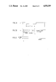
- FIG. 1 is a simplified block diagram of a semiconductor device in accordance with the present invention.
- FIGS. 2A-2C are timing diagrams for explaining the testing operation of the semiconductor device of FIG. 1.
- FIG. 1 shows an LSI chip 1 having an embedded RAM macro 2 in accordance with the invention.
- the RAM macro 2 includes a memory array 4 output latches (sense amplifiers) 6, a control circuit 8, logical gate means 10 and a latch 12.
- the chip 1 further includes interfacing logic circuitry 14, 16, 17, 18. 20, 22 and 24 associated with data inputs, addresses. read/write, macro-select, test strobe, test out and data output lines, respectively.
- the chip 1 further includes receivers 26 and 28, and drivers 30 and 32.
- the read-write line is connected to the array 4 through control circuit 8, and serves to instruct the memory array 4 to perform either a read or write operation.
- the macro-select line extends from receiver 26 to control circuit 8 and to latch 12 through logic circuitry 18.
- a macro-select signal MS supplied on the macro-select line, activates the memory array 4.
- memory array 4 is activated when control circuit 8 receives a "LOW" MS signal.
- the control circuit 8 which alternatively may be provided external to the memory array 4 as a single element, supplies a "HIGH” SL signal to logical gate means 10 in response to a "LOW” MS signal, and supplies a "LOW” SL signal in response to a "HIGH” MS signal.
- the test strobe line extends from receiver 28 to latch 12 and to logical gate means 10 through logic circuitry 20.
- the receiver 28 is adapted to receive a test strobe signal TS from a tester such as a Takeda Riken T3340.
- the test out line extends from latch 12 to driver 30 through logic circuitry 22.
- the data out lines extend from the output latches 6 to drivers 32 through logic 24.
- the logical gate means 10 receives signals SL and TS as inputs, and supplies signal SL as an output to the output latches 6.
- the output latches 6 allow output data to be read out from memory array 4 when signal SL is "HIGH”.
- the logical gate means 10 serves to control the output latches 6 in accordance with signal SL and signal TS. More specifically, logical gate means 10 is designed such that it will supply a "HIGH" SL signal (e.g. output latches 6 enabling signal) only when each of signals SL and TS is "HIGH". Accordingly, logical gate means 10 may be implemented with, for example, an AND gate. Thus, since output latches 6 will only be activated when signal SL is "HIGH”, output data from memory array 4 cannot be latched through output latches 6 until each of signals SL and TS is "HIGH".
- the latch 12 is designed so that it supplies signal MS to the test out line when test strobe TS is "HIGH". This can be accomplished through the use of for example, a clocked D flip-flop, with the signal TS serving as the clock, and signal MS serving as the input to the flip-flop 12.
- the test operation according to the invention includes determining the on-chip delay time T between signals MS and TS. Once the delay time between these signals is determined, it is then possible to verify the access performance of the memory array 4.
- a pulse signal MS is supplied from receiver 26.
- the signal MS has a leading edge (e.g. a transition from 1 to 0) at a user specified time t 1 from origin t.sub. ⁇ .
- the leading edge (LE) of signal MS will serve as a reference portion as will be described below. Since a "LOW" MS signal activates memory array 4, the array 4 becomes active at time t 1 plus the delay through logic circuitry 18.
- signal SL changes from a "LOW" value to a "HIGH” value.
- test strobe TS is supplied with respect to origin t.sub. ⁇ from receiver 28. More specifically, receiver 28 receives test strobe TS from the external tester 34 which is adapted to "schmoo" (see FIG. 2B) signal TS repeatedly until the arrival time of the leading edge of macro-select signal MS is measured at driver 30.
- the schmoo cycle is accomplished by initializing the latch 12 to a "HIGH” value, and then observing the leading edge (LE) or transition of the latched MS signal.
- macro-select signal MS is supplied to D flip-flop 12, and since the test strobe TS serves as the clock for the flip-flop 12, the leading edge of macro-select signal MS will be "captured” or “copied” when the latched MS signal is observed to make a transition from "HIGH” to "LOW” (e.g. LE of MS). With reference to FIGS. 2A-2C the latched MS signal is shown making a transition (e.g. LE of MS captured) with a schmoo cycle ending at time t 2 .
- time t 2 is independent of the time necessary for the latched MS signal to pass through logic 22, since the latched MS signal is merely sampled (e.g. measured) at driver 30 to determine whether the leading edge of signal MS was captured or copied during the schmoo cycle.
- signal TS is first schmoo-ed for a specified time with respect to the origin t.sub. ⁇ , with the trailing edge (TE) of signal TS being set at that specified time.
- the latched MS signal (e.g. output on test out line) is then observed to determine whether the leading edge of signal MS was captured. If the leading edge of signal MS was not captured, then the trailing edge of test strobe signal TS would be incremented (e.g.
- the on-chip delay time T between signals MS and TS can now be calculated by subtracting the timing value of the leading edge of signal MS (t 1 ) from the stored timing value (t 2 ) of the trailing edge of signal TS.
- AC testing Read Access Performance
- time t 1 is 25 ns with respect to the origin t.sub. ⁇
- time t 2 is 40 ns with respect to the origin t.sub. ⁇
- the resulting on-chip delay time T is equal to 15 ns (e.g. 40 ns-25 ns ).
- the manufacturer's specified access time of the memory array 4 is, for example, 10 ns
- a performance test of the access time of the memory array 4 can be run by supplying a "HIGH" TS signal for a time period P equal to the timing value with respect to origin t.sub. ⁇ of the trailing edge of signal TS plus the manufacturer specified access time t m of the memory array.
- the period P for supplying a "HIGH" TS signal is equal to 50 ns (e.g. 40 ns+10 ns).
- the access time of the memory array 4 can be tested since at time t 2 , signals MS and TS are synchronized. More particularly, at time t 2 , array 4 is activated since MS is "LOW", and output latches 6 are enabled since signals SL and TS are each "HIGH”.
- the present invention is able to isolate a macro from intervening logic circuitry so that an accurate timing measurement between a macro-enabling signal and a test input can be implemented during a macro performance test.
- a programmer By latching the data outputs from memory array 4 via signal TS, a programmer is able to control the access time of the macro.
- the on-chip delay time T between signals MS and TS caused by intervening logic circuitry prohibits accurate timing measurement of signals MS and TS during a performance test operation.
- the method and apparatus of the present invention is designed to measure the on-chip delay time T between signals TS and MS, thereby allowing accurate timings to be determined for access time testing of memory array 4.
Abstract
Description
Claims (14)
Priority Applications (4)
| Application Number | Priority Date | Filing Date | Title |
|---|---|---|---|
| US07/169,544 US4878209A (en) | 1988-03-17 | 1988-03-17 | Macro performance test |
| EP89104012A EP0337106B1 (en) | 1988-03-17 | 1989-03-07 | Embedded array access time test |
| DE68924995T DE68924995T2 (en) | 1988-03-17 | 1989-03-07 | Access time check of buried orders. |
| JP1064044A JPH0210278A (en) | 1988-03-17 | 1989-03-17 | Apparatus and method for testing macroaccess time |
Applications Claiming Priority (1)
| Application Number | Priority Date | Filing Date | Title |
|---|---|---|---|
| US07/169,544 US4878209A (en) | 1988-03-17 | 1988-03-17 | Macro performance test |
Publications (1)
| Publication Number | Publication Date |
|---|---|
| US4878209A true US4878209A (en) | 1989-10-31 |
Family
ID=22616147
Family Applications (1)
| Application Number | Title | Priority Date | Filing Date |
|---|---|---|---|
| US07/169,544 Expired - Lifetime US4878209A (en) | 1988-03-17 | 1988-03-17 | Macro performance test |
Country Status (4)
| Country | Link |
|---|---|
| US (1) | US4878209A (en) |
| EP (1) | EP0337106B1 (en) |
| JP (1) | JPH0210278A (en) |
| DE (1) | DE68924995T2 (en) |
Cited By (30)
| Publication number | Priority date | Publication date | Assignee | Title |
|---|---|---|---|---|
| US4982349A (en) * | 1989-06-29 | 1991-01-01 | At&T Bell Laboratories | Response time analysis system |
| US5058087A (en) * | 1987-05-29 | 1991-10-15 | Siemens Aktiengesellschaft | Process for determining the electrical duration of signal paths |
| US5083299A (en) * | 1990-07-16 | 1992-01-21 | Unisys Corporation | Tester for measuring signal propagation delay through electronic components |
| US5181191A (en) * | 1991-11-27 | 1993-01-19 | Hughes Aircraft Company | Built-in test circuitry providing simple and accurate AC test of digital microcircuits with low bandwidth test equipment and probe stations |
| US5268639A (en) * | 1992-06-05 | 1993-12-07 | Rambus, Inc. | Testing timing parameters of high speed integrated circuit devices |
| US5357522A (en) * | 1990-09-28 | 1994-10-18 | Hyundai Electronics Co., Ltd. | Test circuit of input/output macrocell of erasable and programmable logic device |
| US5365165A (en) * | 1986-09-19 | 1994-11-15 | Actel Corporation | Testability architecture and techniques for programmable interconnect architecture |
| US5389990A (en) * | 1989-10-21 | 1995-02-14 | Kabushiki Kaisha Toshiba | Method for measuring DC current/voltage characteristic of semiconductor device |
| US5510730A (en) | 1986-09-19 | 1996-04-23 | Actel Corporation | Reconfigurable programmable interconnect architecture |
| US5528600A (en) * | 1991-01-28 | 1996-06-18 | Actel Corporation | Testability circuits for logic arrays |
| US6005829A (en) * | 1996-09-17 | 1999-12-21 | Xilinx, Inc. | Method for characterizing interconnect timing characteristics |
| US6058496A (en) * | 1997-10-21 | 2000-05-02 | International Business Machines Corporation | Self-timed AC CIO wrap method and apparatus |
| US6069849A (en) * | 1996-09-17 | 2000-05-30 | Xilinx, Inc. | Method and system for measuring signal propagation delays using the duty cycle of a ring oscillator |
| US6075418A (en) * | 1996-09-17 | 2000-06-13 | Xilinx, Inc. | System with downstream set or clear for measuring signal propagation delays on integrated circuits |
| US6144262A (en) * | 1996-09-17 | 2000-11-07 | Xilinx, Inc. | Circuit for measuring signal delays of asynchronous register inputs |
| US6219305B1 (en) | 1996-09-17 | 2001-04-17 | Xilinx, Inc. | Method and system for measuring signal propagation delays using ring oscillators |
| US6232845B1 (en) | 1996-09-17 | 2001-05-15 | Xilinx, Inc. | Circuit for measuring signal delays in synchronous memory elements |
| US6233205B1 (en) | 1996-09-17 | 2001-05-15 | Xilinx, Inc. | Built-in self test method for measuring clock to out delays |
| US6327224B1 (en) | 2000-06-16 | 2001-12-04 | International Business Machines Corporation | On-chip method for measuring access time and data-pin spread |
| US6356513B1 (en) * | 1998-05-29 | 2002-03-12 | Stmicroelectronics S.R.L. | Additional probe circuit for measuring delay time in embedded circuits |
| US6437597B1 (en) | 2001-04-11 | 2002-08-20 | Xilinx, Inc. | Methods and circuits for precise edge placement of test signals |
| US6452459B1 (en) | 1999-07-22 | 2002-09-17 | Xilinx, Inc. | Circuit for measuring signal delays of synchronous memory elements |
| US6466520B1 (en) | 1996-09-17 | 2002-10-15 | Xilinx, Inc. | Built-in AC self test using pulse generators |
| US6630838B1 (en) | 2001-01-23 | 2003-10-07 | Xilinx, Inc. | Method for implementing dynamic burn-in testing using static test signals |
| US7031864B2 (en) * | 2000-07-18 | 2006-04-18 | Oki Electric Industry Co., Ltd. | Semiconductor device having a mode of functional test |
| US7065684B1 (en) | 2002-04-18 | 2006-06-20 | Xilinx, Inc. | Circuits and methods for measuring signal propagation delays on integrated circuits |
| US20060190782A1 (en) * | 2005-02-22 | 2006-08-24 | International Business Machines Corporation | Mechanism to provide test access to third-party macro circuits embedded in an asic (application-specific integrated circuit) |
| US20060190215A1 (en) * | 2005-02-18 | 2006-08-24 | Taiwan Semiconductor Manufacturing Co., Ltd. | Method and system for timing measurement of embedded macro module |
| US20080231307A1 (en) * | 2007-03-21 | 2008-09-25 | Bickford Jeanne P | Testing method using a scalable parametric measurement macro |
| FR3110261A1 (en) * | 2020-05-18 | 2021-11-19 | Idemia Starchip | METHOD AND SYSTEM FOR TESTING AN INTEGRATED CIRCUIT |
Families Citing this family (5)
| Publication number | Priority date | Publication date | Assignee | Title |
|---|---|---|---|---|
| US5455517A (en) * | 1992-06-09 | 1995-10-03 | International Business Machines Corporation | Data output impedance control |
| CA2099415A1 (en) * | 1992-08-27 | 1994-02-28 | Duane Rodney Aadsen | Method and apparatus for self-testing of delay faults |
| EP0845788B1 (en) * | 1996-11-27 | 2003-09-10 | Texas Instruments Incorporated | A memory array test circuit with failure notification |
| KR100517257B1 (en) * | 1996-11-27 | 2005-11-28 | 텍사스 인스트루먼츠 인코포레이티드 | Memory array test circuit and method |
| DE19711097C2 (en) * | 1997-03-17 | 2000-04-06 | Siemens Ag | Integrated circuit with a memory and a test circuit |
Citations (13)
| Publication number | Priority date | Publication date | Assignee | Title |
|---|---|---|---|---|
| US3961251A (en) * | 1974-12-20 | 1976-06-01 | International Business Machines Corporation | Testing embedded arrays |
| US3961252A (en) * | 1974-12-20 | 1976-06-01 | International Business Machines Corporation | Testing embedded arrays |
| US3961254A (en) * | 1974-12-20 | 1976-06-01 | International Business Machines Corporation | Testing embedded arrays |
| US4058767A (en) * | 1975-04-29 | 1977-11-15 | International Business Machines Corporation | Apparatus and process for testing AC performance of LSI components |
| US4225957A (en) * | 1978-10-16 | 1980-09-30 | International Business Machines Corporation | Testing macros embedded in LSI chips |
| US4332028A (en) * | 1979-06-29 | 1982-05-25 | International Business Machines Corporation | Method of measuring the memory address access time (AAT) utilizing a data recirculation technique, and a tester for accomplishing same |
| US4461000A (en) * | 1982-03-01 | 1984-07-17 | Harris Corporation | ROM/PLA Structure and method of testing |
| US4481627A (en) * | 1981-10-30 | 1984-11-06 | Honeywell Information Systems Inc. | Embedded memory testing method and apparatus |
| US4482953A (en) * | 1980-05-30 | 1984-11-13 | Fairchild Camera & Instrument Corporation | Computer with console addressable PLA storing control microcode and microinstructions for self-test of internal registers and ALU |
| US4503387A (en) * | 1982-12-30 | 1985-03-05 | Harris Corporation | A.C. Testing of logic arrays |
| US4510603A (en) * | 1981-05-26 | 1985-04-09 | Burroughs Corporation | Testing system for reliable access times in ROM semiconductor memories |
| US4513418A (en) * | 1982-11-08 | 1985-04-23 | International Business Machines Corporation | Simultaneous self-testing system |
| US4608669A (en) * | 1984-05-18 | 1986-08-26 | International Business Machines Corporation | Self contained array timing |
Family Cites Families (3)
| Publication number | Priority date | Publication date | Assignee | Title |
|---|---|---|---|---|
| US4430735A (en) * | 1981-05-26 | 1984-02-07 | Burroughs Corporation | Apparatus and technique for testing IC memories |
| JPH0711559B2 (en) * | 1983-11-07 | 1995-02-08 | 株式会社日立製作所 | Test pattern generator |
| JPS6122500A (en) * | 1984-07-09 | 1986-01-31 | Advantest Corp | Ic testing device |
-
1988
- 1988-03-17 US US07/169,544 patent/US4878209A/en not_active Expired - Lifetime
-
1989
- 1989-03-07 DE DE68924995T patent/DE68924995T2/en not_active Expired - Fee Related
- 1989-03-07 EP EP89104012A patent/EP0337106B1/en not_active Expired - Lifetime
- 1989-03-17 JP JP1064044A patent/JPH0210278A/en active Pending
Patent Citations (13)
| Publication number | Priority date | Publication date | Assignee | Title |
|---|---|---|---|---|
| US3961252A (en) * | 1974-12-20 | 1976-06-01 | International Business Machines Corporation | Testing embedded arrays |
| US3961254A (en) * | 1974-12-20 | 1976-06-01 | International Business Machines Corporation | Testing embedded arrays |
| US3961251A (en) * | 1974-12-20 | 1976-06-01 | International Business Machines Corporation | Testing embedded arrays |
| US4058767A (en) * | 1975-04-29 | 1977-11-15 | International Business Machines Corporation | Apparatus and process for testing AC performance of LSI components |
| US4225957A (en) * | 1978-10-16 | 1980-09-30 | International Business Machines Corporation | Testing macros embedded in LSI chips |
| US4332028A (en) * | 1979-06-29 | 1982-05-25 | International Business Machines Corporation | Method of measuring the memory address access time (AAT) utilizing a data recirculation technique, and a tester for accomplishing same |
| US4482953A (en) * | 1980-05-30 | 1984-11-13 | Fairchild Camera & Instrument Corporation | Computer with console addressable PLA storing control microcode and microinstructions for self-test of internal registers and ALU |
| US4510603A (en) * | 1981-05-26 | 1985-04-09 | Burroughs Corporation | Testing system for reliable access times in ROM semiconductor memories |
| US4481627A (en) * | 1981-10-30 | 1984-11-06 | Honeywell Information Systems Inc. | Embedded memory testing method and apparatus |
| US4461000A (en) * | 1982-03-01 | 1984-07-17 | Harris Corporation | ROM/PLA Structure and method of testing |
| US4513418A (en) * | 1982-11-08 | 1985-04-23 | International Business Machines Corporation | Simultaneous self-testing system |
| US4503387A (en) * | 1982-12-30 | 1985-03-05 | Harris Corporation | A.C. Testing of logic arrays |
| US4608669A (en) * | 1984-05-18 | 1986-08-26 | International Business Machines Corporation | Self contained array timing |
Cited By (45)
| Publication number | Priority date | Publication date | Assignee | Title |
|---|---|---|---|---|
| US5365165A (en) * | 1986-09-19 | 1994-11-15 | Actel Corporation | Testability architecture and techniques for programmable interconnect architecture |
| US5510730A (en) | 1986-09-19 | 1996-04-23 | Actel Corporation | Reconfigurable programmable interconnect architecture |
| US5432441A (en) * | 1986-09-19 | 1995-07-11 | Actel Corporation | Testability architecture and techniques for programmable interconnect architecture |
| US5058087A (en) * | 1987-05-29 | 1991-10-15 | Siemens Aktiengesellschaft | Process for determining the electrical duration of signal paths |
| US4982349A (en) * | 1989-06-29 | 1991-01-01 | At&T Bell Laboratories | Response time analysis system |
| US5389990A (en) * | 1989-10-21 | 1995-02-14 | Kabushiki Kaisha Toshiba | Method for measuring DC current/voltage characteristic of semiconductor device |
| US5083299A (en) * | 1990-07-16 | 1992-01-21 | Unisys Corporation | Tester for measuring signal propagation delay through electronic components |
| US5357522A (en) * | 1990-09-28 | 1994-10-18 | Hyundai Electronics Co., Ltd. | Test circuit of input/output macrocell of erasable and programmable logic device |
| US5528600A (en) * | 1991-01-28 | 1996-06-18 | Actel Corporation | Testability circuits for logic arrays |
| US5614818A (en) * | 1991-01-28 | 1997-03-25 | Actel Corporation | Testability circuits for logic circuit arrays |
| US5804960A (en) * | 1991-01-28 | 1998-09-08 | Actel Corporation | Circuits for testing the function circuit modules in an integrated circuit |
| US5181191A (en) * | 1991-11-27 | 1993-01-19 | Hughes Aircraft Company | Built-in test circuitry providing simple and accurate AC test of digital microcircuits with low bandwidth test equipment and probe stations |
| US5357195A (en) * | 1992-06-05 | 1994-10-18 | Rambus, Inc. | Testing set up and hold input timing parameters of high speed integrated circuit devices |
| US5325053A (en) * | 1992-06-05 | 1994-06-28 | Rambus, Inc. | Apparatus for testing timing parameters of high speed integrated circuit devices |
| US5268639A (en) * | 1992-06-05 | 1993-12-07 | Rambus, Inc. | Testing timing parameters of high speed integrated circuit devices |
| US6233205B1 (en) | 1996-09-17 | 2001-05-15 | Xilinx, Inc. | Built-in self test method for measuring clock to out delays |
| US6466520B1 (en) | 1996-09-17 | 2002-10-15 | Xilinx, Inc. | Built-in AC self test using pulse generators |
| US6069849A (en) * | 1996-09-17 | 2000-05-30 | Xilinx, Inc. | Method and system for measuring signal propagation delays using the duty cycle of a ring oscillator |
| US6075418A (en) * | 1996-09-17 | 2000-06-13 | Xilinx, Inc. | System with downstream set or clear for measuring signal propagation delays on integrated circuits |
| US6144262A (en) * | 1996-09-17 | 2000-11-07 | Xilinx, Inc. | Circuit for measuring signal delays of asynchronous register inputs |
| US6219305B1 (en) | 1996-09-17 | 2001-04-17 | Xilinx, Inc. | Method and system for measuring signal propagation delays using ring oscillators |
| US6232845B1 (en) | 1996-09-17 | 2001-05-15 | Xilinx, Inc. | Circuit for measuring signal delays in synchronous memory elements |
| US6005829A (en) * | 1996-09-17 | 1999-12-21 | Xilinx, Inc. | Method for characterizing interconnect timing characteristics |
| US6611477B1 (en) | 1996-09-17 | 2003-08-26 | Xilinx, Inc. | Built-in self test using pulse generators |
| US6356514B1 (en) | 1996-09-17 | 2002-03-12 | Xilinx, Inc. | Built-in self test method for measuring clock to out delays |
| US6058496A (en) * | 1997-10-21 | 2000-05-02 | International Business Machines Corporation | Self-timed AC CIO wrap method and apparatus |
| US6356513B1 (en) * | 1998-05-29 | 2002-03-12 | Stmicroelectronics S.R.L. | Additional probe circuit for measuring delay time in embedded circuits |
| US6452459B1 (en) | 1999-07-22 | 2002-09-17 | Xilinx, Inc. | Circuit for measuring signal delays of synchronous memory elements |
| US6327224B1 (en) | 2000-06-16 | 2001-12-04 | International Business Machines Corporation | On-chip method for measuring access time and data-pin spread |
| US7484135B2 (en) | 2000-07-18 | 2009-01-27 | Oki Electric Industry Co., Ltd. | Semiconductor device having a mode of functional test |
| US20060149500A1 (en) * | 2000-07-18 | 2006-07-06 | Katsuaki Matsui | Semiconductor device having a mode of functional test |
| US7031864B2 (en) * | 2000-07-18 | 2006-04-18 | Oki Electric Industry Co., Ltd. | Semiconductor device having a mode of functional test |
| US6630838B1 (en) | 2001-01-23 | 2003-10-07 | Xilinx, Inc. | Method for implementing dynamic burn-in testing using static test signals |
| US6437597B1 (en) | 2001-04-11 | 2002-08-20 | Xilinx, Inc. | Methods and circuits for precise edge placement of test signals |
| US7065684B1 (en) | 2002-04-18 | 2006-06-20 | Xilinx, Inc. | Circuits and methods for measuring signal propagation delays on integrated circuits |
| US20060190215A1 (en) * | 2005-02-18 | 2006-08-24 | Taiwan Semiconductor Manufacturing Co., Ltd. | Method and system for timing measurement of embedded macro module |
| US7212939B2 (en) * | 2005-02-18 | 2007-05-01 | Taiwan Semiconductor Manufacturin Co., Ltd. | Method and system for timing measurement of embedded macro module |
| CN100517515C (en) * | 2005-02-18 | 2009-07-22 | 台湾积体电路制造股份有限公司 | Method and system for measurement |
| US20060190782A1 (en) * | 2005-02-22 | 2006-08-24 | International Business Machines Corporation | Mechanism to provide test access to third-party macro circuits embedded in an asic (application-specific integrated circuit) |
| US7308630B2 (en) | 2005-02-22 | 2007-12-11 | International Business Machines Corporation | Mechanism to provide test access to third-party macro circuits embedded in an ASIC (application-specific integrated circuit) |
| US20080022171A1 (en) * | 2005-02-22 | 2008-01-24 | Grupp Richard J | Mechanism to provide test access to third-party macro circuits embedded in an asic (application-specific integrated circuit) |
| US7734968B2 (en) | 2005-02-22 | 2010-06-08 | International Business Machines Corporation | Mechanism to provide test access to third-party macro circuits embedded in an ASIC (application-specific integrated circuit) |
| US20080231307A1 (en) * | 2007-03-21 | 2008-09-25 | Bickford Jeanne P | Testing method using a scalable parametric measurement macro |
| US7656182B2 (en) | 2007-03-21 | 2010-02-02 | International Business Machines Corporation | Testing method using a scalable parametric measurement macro |
| FR3110261A1 (en) * | 2020-05-18 | 2021-11-19 | Idemia Starchip | METHOD AND SYSTEM FOR TESTING AN INTEGRATED CIRCUIT |
Also Published As
| Publication number | Publication date |
|---|---|
| DE68924995T2 (en) | 1996-06-20 |
| JPH0210278A (en) | 1990-01-16 |
| EP0337106A3 (en) | 1991-07-03 |
| EP0337106A2 (en) | 1989-10-18 |
| DE68924995D1 (en) | 1996-01-18 |
| EP0337106B1 (en) | 1995-12-06 |
Similar Documents
| Publication | Publication Date | Title |
|---|---|---|
| US4878209A (en) | Macro performance test | |
| EP0161639B1 (en) | Self contained array timing | |
| US6122762A (en) | Memory interface device and method for supporting debugging | |
| Huang et al. | A programmable BIST core for embedded DRAM | |
| US5822228A (en) | Method for using built in self test to characterize input-to-output delay time of embedded cores and other integrated circuits | |
| US7870454B2 (en) | Structure for system for and method of performing high speed memory diagnostics via built-in-self-test | |
| US5761215A (en) | Scan based path delay testing of integrated circuits containing embedded memory elements | |
| US5394403A (en) | Fully testable chip having self-timed memory arrays | |
| US5386392A (en) | Programmable high speed array clock generator circuit for array built-in self test memory chips | |
| US7607060B2 (en) | System and method for performing high speed memory diagnostics via built-in-self-test | |
| US20090116312A1 (en) | Storage Array Including a Local Clock Buffer with Programmable Timing | |
| US5513186A (en) | Method and apparatus for interconnect testing without speed degradation | |
| EP0895245B1 (en) | Synchronous semiconductor memory device | |
| US6060898A (en) | Format sensitive timing calibration for an integrated circuit tester | |
| US6275428B1 (en) | Memory-embedded semiconductor integrated circuit device and method for testing same | |
| US6479363B1 (en) | Semiconductor integrated circuit and method for testing the same | |
| US6341092B1 (en) | Designing memory for testability to support scan capability in an asic design | |
| KR100776855B1 (en) | Arrangement for generating signal pulses with defined pulse length in a module with bist-function | |
| US6643809B2 (en) | Semiconductor device and semiconductor device testing method | |
| US7227810B2 (en) | Semiconductor device and testing method for semiconductor device | |
| US6158029A (en) | Method of testing an integrated circuit having a memory and a test circuit | |
| JPH04274100A (en) | Memory-lsi with built-in test circuit | |
| US6198700B1 (en) | Method and apparatus for retiming test signals | |
| JPS62103894A (en) | Reading end signal generation circuit | |
| US6973422B1 (en) | Method and apparatus for modeling and circuits with asynchronous behavior |
Legal Events
| Date | Code | Title | Description |
|---|---|---|---|
| AS | Assignment |
Owner name: INTERNATIONAL BUSINESS MACHINES CORPORATION, ARMON Free format text: ASSIGNMENT OF ASSIGNORS INTEREST.;ASSIGNORS:BASSETT, ROBERT W.;GRIFFIN, WILLIAM R.;MURPHY, SUSAN A.;AND OTHERS;REEL/FRAME:004880/0625;SIGNING DATES FROM 19880303 TO 19880310 Owner name: INTERNATIONAL BUSINESS MACHINES CORPORATION, A COR Free format text: ASSIGNMENT OF ASSIGNORS INTEREST;ASSIGNORS:BASSETT, ROBERT W.;GRIFFIN, WILLIAM R.;MURPHY, SUSAN A.;AND OTHERS;SIGNING DATES FROM 19880303 TO 19880310;REEL/FRAME:004880/0625 |
|
| STCF | Information on status: patent grant |
Free format text: PATENTED CASE |
|
| FEPP | Fee payment procedure |
Free format text: PAYOR NUMBER ASSIGNED (ORIGINAL EVENT CODE: ASPN); ENTITY STATUS OF PATENT OWNER: LARGE ENTITY |
|
| FPAY | Fee payment |
Year of fee payment: 4 |
|
| FPAY | Fee payment |
Year of fee payment: 8 |
|
| FEPP | Fee payment procedure |
Free format text: PAYER NUMBER DE-ASSIGNED (ORIGINAL EVENT CODE: RMPN); ENTITY STATUS OF PATENT OWNER: LARGE ENTITY |
|
| FPAY | Fee payment |
Year of fee payment: 12 |