US4882506A - Low voltage and low power detector circuits - Google Patents

Low voltage and low power detector circuits Download PDF

Info

Publication number
US4882506A
US4882506A US06/908,536 US90853686A US4882506A US 4882506 A US4882506 A US 4882506A US 90853686 A US90853686 A US 90853686A US 4882506 A US4882506 A US 4882506A
Authority
US
United States
Prior art keywords
low
voltage
output
low voltage
comparator
Prior art date
Legal status (The legal status is an assumption and is not a legal conclusion. Google has not performed a legal analysis and makes no representation as to the accuracy of the status listed.)
Expired - Lifetime
Application number
US06/908,536
Inventor
Jan H. Johansson
Erik K. Lunderius
Current Assignee (The listed assignees may be inaccurate. Google has not performed a legal analysis and makes no representation or warranty as to the accuracy of the list.)
Advanced Micro Devices Inc
Original Assignee
Advanced Micro Devices Inc
Priority date (The priority date is an assumption and is not a legal conclusion. Google has not performed a legal analysis and makes no representation as to the accuracy of the date listed.)
Filing date
Publication date
Application filed by Advanced Micro Devices Inc filed Critical Advanced Micro Devices Inc
Priority to US06/908,536 priority Critical patent/US4882506A/en
Priority to JP62505817A priority patent/JPH01500874A/en
Priority to PCT/US1987/002370 priority patent/WO1988002204A1/en
Priority to EP19870906372 priority patent/EP0282567A4/en
Assigned to ADVANCED MICRO DEVICES, INC. reassignment ADVANCED MICRO DEVICES, INC. ASSIGNMENT OF ASSIGNORS INTEREST. Assignors: JOHANSSON, JAN H., LUNDERIUS, ERIK K.
Application granted granted Critical
Publication of US4882506A publication Critical patent/US4882506A/en
Anticipated expiration legal-status Critical
Expired - Lifetime legal-status Critical Current

Links

Images

Classifications

    • HELECTRICITY
    • H04ELECTRIC COMMUNICATION TECHNIQUE
    • H04MTELEPHONIC COMMUNICATION
    • H04M19/00Current supply arrangements for telephone systems
    • H04M19/08Current supply arrangements for telephone systems with current supply sources at the substations
    • YGENERAL TAGGING OF NEW TECHNOLOGICAL DEVELOPMENTS; GENERAL TAGGING OF CROSS-SECTIONAL TECHNOLOGIES SPANNING OVER SEVERAL SECTIONS OF THE IPC; TECHNICAL SUBJECTS COVERED BY FORMER USPC CROSS-REFERENCE ART COLLECTIONS [XRACs] AND DIGESTS
    • Y02TECHNOLOGIES OR APPLICATIONS FOR MITIGATION OR ADAPTATION AGAINST CLIMATE CHANGE
    • Y02DCLIMATE CHANGE MITIGATION TECHNOLOGIES IN INFORMATION AND COMMUNICATION TECHNOLOGIES [ICT], I.E. INFORMATION AND COMMUNICATION TECHNOLOGIES AIMING AT THE REDUCTION OF THEIR OWN ENERGY USE
    • Y02D30/00Reducing energy consumption in communication networks
    • Y02D30/70Reducing energy consumption in communication networks in wireless communication networks

Definitions

  • This invention relates generally to detection circuits and more particularly, it relates to low voltage and low power detection circuits for use in a subscriber power controller integrated circuit which permits communication across the S interface of the Integrated Services Digital Network (ISDN).
  • ISDN Integrated Services Digital Network
  • the S or subscriber lines interface as referred to by the Consultative Committee for International Circuity and Telephony (CCITT) is used to interconnect ISDN terminal equipment to one or more network terminators such as private branch exchanges (PBX).
  • PBX private branch exchanges
  • a subscriber power controller (SPC) is used to convert the 40 volts delivered at the S interface into a stable, regulated 5 volt power supply for integrated circuits in the ISDN terminal equipment such as a telephone or data generating equipment.
  • SPC subscriber power controller
  • Such a power controller is manufactured and sold by Advanced Micro Devices, Inc., Sunnyvale, California, under part No.
  • the subscriber power controller is an integrated circuit formed of a single-chip package. As a part of the subscriber power controller integrated circuit, there are provided circuits which function to detect and to protect against certain faults most likely to occur at the S interface. In particular, the subscriber power controller is safeguarded against a low input voltage and a low input power.
  • the low voltage and low power detection circuits of the present invention is provided as a part of the subscriber power controller integrated circuit for performing such fault detecting functions.
  • the subscriber power controller When the primary input supply voltage drops below a certain preset value, the subscriber power controller is disabled so as to prevent the supply line from being loaded down to an unacceptable low voltage level. Further, when the primary input supply voltage drops below a certain level a microprocessor is informed that the input power is low so as to permit disconnecting of all high power functions in order to conserve power.
  • low voltage and low power circuits of the present invention are provided for use in a subscriber power controller which includes a low voltage detection circuit for generating a first output signal switching between ECL logic levels and a low power detection circuit for generating a second output signal switching between a high voltage level and a low voltage level.
  • the low voltage detection circuit is formed of a first comparator with hysteresis and a first output stage.
  • the first comparator compares a low voltage detection signal corresponding to a portion of a primary input supply voltage with an internal reference voltage to produce a first detected signal.
  • the first output stage is responsive to the first detected signal to produce the first output signal.
  • the low power detection circuit is formed of a second comparator with hysteresis and a second output stage.
  • the second comparator compares a lower power detection signal corresponding to a portion of the primary input supply voltage with the internal reference voltage to produce a second detected signal.
  • the second output stage is responsive to the second detected signal to produce the second output signal.
  • FIG. 1 is an overall block diagram of an integrated services digital network for communication across the S interface in accordance with the present invention
  • FIG. 2 is a more detailed block diagram of the subscriber power controller block in FIG. 1;
  • FIG. 3 is a detailed schematic circuit diagram of the low voltage detection circuit in the subscriber power controller of FIG. 2;
  • FIG. 4 is a detailed schematic circuit diagram of the low power detection circuit of the subscriber power controller of FIG. 2.
  • FIG. 1 an overall block diagram of an integrated services digital network (ISDN) for communication across the S or subscriber interface which connects terminal equipment 2 to a network terminator 3 such as a private branch exchange (PBX).
  • the terminal equipment 2 includes a digital subscriber controller 5, a microprocessor 6, and a subscriber power controller 7.
  • the subscriber power controller is an integrated circuit which converts the 40 volts delivered at the S interface into a stable, regulated 5 volt power supply for other chips in the ISDN terminal equipment.
  • FIG. 2 a more detailed block diagram of the subscriber power controller 7 is illustrated.
  • a controller is the Am7936 subscriber power controller manufactured by Advanced Micro Devices, Inc. of Sunnyvale, California.
  • the controller 7 includes a low voltage detection circuit 12 of the present invention which senses a portion of the primary input supply voltage VIN and compares it with a reference voltage REF1. When the sensed or detected voltage drops below the reference voltage REF1, the subscriber power controller 7 is disabled, thereby preventing the supply lines 14, 16, from being loaded down to an unacceptable low voltage level.
  • the subscriber power controller is disabled by a control logic block 18 which receives as one of its input the output on line 20 from the low voltage detection circuit 12.
  • the controller 7 also includes a low power detection circuit 22 of the present invention which monitors the primary input supply voltage VIN and compares it with an internal reference voltage REF2. When the input voltage drops below the reference voltage REF2, a high voltage level appears on the line 24 at the output of the low power detection circuit 22, and is sent to the microprocessor 6 to indicate an emergency power condition so that all high power functions may be disabled or turned off so as to conserve power.
  • FIG. 3 there is shown a detailed schematic circuit diagram of the low voltage detection circuit 12 formed of a comparator stage 24 with hysteresis and a logic output stage 26.
  • the comparator stage 24 comprises a differential amplifier formed of a pair of transistors Q4 and Q14, a current source transistor Q15 to supply a bias current, a current mirror formed of transistors Q7 and Q8, and an output transistor Q9.
  • the comparator 24 has a first inverting input terminal 28 which is connected to receive a low voltage detection signal for delivery to the base of the transistor Q1.
  • the comparator 24 has a second inverting input terminal 30 which is connected to receive another input signal which may be used to set another voltage reference level.
  • the inverting input terminal 32 of the comparator 24 is connected to receive a reference voltage REF1 which is applied to the base of the transistor Q6.
  • the output of the comparator 24 is taken from the collector of the output transistor Q9.
  • the differential voltage VDIFF1 across the first inverting input terminal 28 and the non-inverting terminal 32 will be at a negative potential. This causes the the transistors Q1 and Q3 to be turned off and causes the transistors Q6 and Q14 to be turned off. As a result, the output transistor Q9 will be turned off rendering its collector to be at a high voltage level. As the differential voltage VDIFF increases and becomes positive corresponding to a detected low voltage signal, the transistors Q1 and Q3 will become non-conductive and the transistors Q6 and Q14 will be turned on so as to supply current to the base of the output transistor Q9. Thus, the transistor Q9 will be saturated and the output of the comparator 24 at the collector of the transistor Q9 will be at a low voltage level representing the detection of a low voltage from the primary input supply voltage VIN.
  • the logic output stage 26 comprises a multi-emitter transistor Q11 and emitter follower transistors Q12 and Q13.
  • the input of the logic output stage 26 is at the base of the transistor Q11 which is connected to the output of the comparator 24 at the collector of transistor Q9.
  • the emitters 34, 36 and 38 are the outputs of output stage 24 and operate at ECL logic levels.
  • the emitter 40 provides a logic output which is connected to the bases of transistors Q12 and Q13 so as to provide an additional ECL logic output at the output terminal 42.
  • the logic outputs at the emitters 34-40 will be at a low ECL logic level.
  • the logic outputs at the emitters 34-36 will be at a high ECL logic level.
  • FIG. 4 there is shown a detailed schematic circuit diagram of the low power detection circuit 22 formed of a comparator stage 42 with hysteresis and an output stage 44.
  • the comparator stage 42 comprises a differential amplifier formed of a pair of transistors Q103 and Q104, a current source Q107 to supply a bias current, a current mirror formed of transistors Q108 and Q109, and an output transistor Q110.
  • the comparator 42 has a non-inverting input terminal 46 which is connected to receive a low power detection signal for delivery to the base of the transistor Q106.
  • the comparator has an inverting input terminal 48 which is connected to receive a reference voltage REF2 for delivery to the base of the transistor Q101.
  • the output of the comparator 42 is taken from the collector of the transistor Q110.
  • the differential voltage VDIFF2 across the inverting terminal 48 and the non-inverting input terminal 46 will be at a negative voltage potential.
  • This causes the transistors Q101-Q103 to be turned on and the transistors Q104-Q106 to be turned off.
  • the output transistor Q110 will be turned off rendering its collector to be at a high voltage level.
  • the differential voltage VDIFF2 increases and becomes positive indicating detection of a low power signal
  • the transistors Q101-Q103 will become non-conductive and the transistors Q104-Q106 will be turned on and supply current to the base of the output transistor Q110.
  • the transistor Q110 will be saturated and the output at its collector will be at a low voltage level, representing the detected low power appearing at the primary input supply voltage VIN.
  • the output stage 44 comprises a current mirror formed of transistors Q111 and Q112, a transistor Q113, an output transistor Q114, and a current source transistor Q115.
  • the input of the output stage 44 is at the junction of the base-collector of the transistor Q111 and the base of the transistor Q112 which is connected to the output of the comparator stage 42 at the collector of the transistor Q110.
  • the output of the output stage 44 is taken from the collector of the transistor Q114.
  • the output at the collector of the transistor Q114 will be at a low voltage level which is approximately +35 volts.
  • the output at the collector of the transistor Q114 will be at a high voltage level which is approximately +40 volts.
  • the present invention provides a low voltage and low power detection circuits for use in a subscriber power controller which includes a low voltage detection circuit for generating a first output signal switching between ECL logic levels and a low power detection circuit for generating a second output signal switching between a high voltage level and a low voltage level.
  • the first output signal is used to disable the controller when the primary input voltage drops below a certain preset level.
  • the second output signal has no influence on the controller but is used to inform a microprocessor that a low power has been detected on the primary input supply voltage so as to disable all high power functions in order to conserve power.

Abstract

Low voltage and low power circuits for use in a subscriber power controller includes a low voltage detection circuit for generating a first output signal switching between ECL logic levels and a low power detection circuit for generating a second output signal switching between a high voltage level and a low voltage level. The low voltage detection circuit is formed of a first comparator with hysteresis and a first output stage. The low power detection circuit is formed of a second comparator with hysteresis and a second output stage. The first output signal is used to disable the controller upon detection of a low voltage at the primary input signal voltage. The second output signal is used to inform a microprocessor so as to permit it to disable all high power functions in order to conserve power.

Description

BACKGROUND OF THE INVENTION
This invention relates generally to detection circuits and more particularly, it relates to low voltage and low power detection circuits for use in a subscriber power controller integrated circuit which permits communication across the S interface of the Integrated Services Digital Network (ISDN).
In the field of telecommunications, use of digital signalling techniques in transmitting information over long distances is gaining more and more prominence for a wide range of communication, including voice, computer data and video data. Typically, the S or subscriber lines interface as referred to by the Consultative Committee for International Telegraphy and Telephony (CCITT) is used to interconnect ISDN terminal equipment to one or more network terminators such as private branch exchanges (PBX). A subscriber power controller (SPC) is used to convert the 40 volts delivered at the S interface into a stable, regulated 5 volt power supply for integrated circuits in the ISDN terminal equipment such as a telephone or data generating equipment. Such a power controller is manufactured and sold by Advanced Micro Devices, Inc., Sunnyvale, California, under part No. Am37936. The subscriber power controller is an integrated circuit formed of a single-chip package. As a part of the subscriber power controller integrated circuit, there are provided circuits which function to detect and to protect against certain faults most likely to occur at the S interface. In particular, the subscriber power controller is safeguarded against a low input voltage and a low input power.
The low voltage and low power detection circuits of the present invention is provided as a part of the subscriber power controller integrated circuit for performing such fault detecting functions. When the primary input supply voltage drops below a certain preset value, the subscriber power controller is disabled so as to prevent the supply line from being loaded down to an unacceptable low voltage level. Further, when the primary input supply voltage drops below a certain level a microprocessor is informed that the input power is low so as to permit disconnecting of all high power functions in order to conserve power.
SUMMARY OF THE INVENTION
In a preferred embodiment, low voltage and low power circuits of the present invention are provided for use in a subscriber power controller which includes a low voltage detection circuit for generating a first output signal switching between ECL logic levels and a low power detection circuit for generating a second output signal switching between a high voltage level and a low voltage level. The low voltage detection circuit is formed of a first comparator with hysteresis and a first output stage. The first comparator compares a low voltage detection signal corresponding to a portion of a primary input supply voltage with an internal reference voltage to produce a first detected signal. The first output stage is responsive to the first detected signal to produce the first output signal.
The low power detection circuit is formed of a second comparator with hysteresis and a second output stage. The second comparator compares a lower power detection signal corresponding to a portion of the primary input supply voltage with the internal reference voltage to produce a second detected signal. The second output stage is responsive to the second detected signal to produce the second output signal.
BRIEF DESCRIPTION OF THE DRAWINGS
The present invention will be better understood from the following detailed description when read in conjunction with the accompanying drawings with like reference numerals indicating corresponding parts throughout, wherein:
FIG. 1 is an overall block diagram of an integrated services digital network for communication across the S interface in accordance with the present invention;
FIG. 2 is a more detailed block diagram of the subscriber power controller block in FIG. 1;
FIG. 3 is a detailed schematic circuit diagram of the low voltage detection circuit in the subscriber power controller of FIG. 2; and
FIG. 4 is a detailed schematic circuit diagram of the low power detection circuit of the subscriber power controller of FIG. 2.
DESCRIPTION OF THE PREFERRED EMBODIMENT
Referring now in detail to the drawings, there is shown in FIG. 1 an overall block diagram of an integrated services digital network (ISDN) for communication across the S or subscriber interface which connects terminal equipment 2 to a network terminator 3 such as a private branch exchange (PBX). The terminal equipment 2 includes a digital subscriber controller 5, a microprocessor 6, and a subscriber power controller 7. As previously explained, the subscriber power controller is an integrated circuit which converts the 40 volts delivered at the S interface into a stable, regulated 5 volt power supply for other chips in the ISDN terminal equipment.
As can be seen from FIG. 2, a more detailed block diagram of the subscriber power controller 7 is illustrated. Such a controller is the Am7936 subscriber power controller manufactured by Advanced Micro Devices, Inc. of Sunnyvale, California. The controller 7 includes a low voltage detection circuit 12 of the present invention which senses a portion of the primary input supply voltage VIN and compares it with a reference voltage REF1. When the sensed or detected voltage drops below the reference voltage REF1, the subscriber power controller 7 is disabled, thereby preventing the supply lines 14, 16, from being loaded down to an unacceptable low voltage level. The subscriber power controller is disabled by a control logic block 18 which receives as one of its input the output on line 20 from the low voltage detection circuit 12.
The controller 7 also includes a low power detection circuit 22 of the present invention which monitors the primary input supply voltage VIN and compares it with an internal reference voltage REF2. When the input voltage drops below the reference voltage REF2, a high voltage level appears on the line 24 at the output of the low power detection circuit 22, and is sent to the microprocessor 6 to indicate an emergency power condition so that all high power functions may be disabled or turned off so as to conserve power.
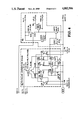
In FIG. 3, there is shown a detailed schematic circuit diagram of the low voltage detection circuit 12 formed of a comparator stage 24 with hysteresis and a logic output stage 26. The comparator stage 24 comprises a differential amplifier formed of a pair of transistors Q4 and Q14, a current source transistor Q15 to supply a bias current, a current mirror formed of transistors Q7 and Q8, and an output transistor Q9. The comparator 24 has a first inverting input terminal 28 which is connected to receive a low voltage detection signal for delivery to the base of the transistor Q1. The comparator 24 has a second inverting input terminal 30 which is connected to receive another input signal which may be used to set another voltage reference level.
The inverting input terminal 32 of the comparator 24 is connected to receive a reference voltage REF1 which is applied to the base of the transistor Q6. The output of the comparator 24 is taken from the collector of the output transistor Q9.
Normally, the differential voltage VDIFF1 across the first inverting input terminal 28 and the non-inverting terminal 32 will be at a negative potential. This causes the the transistors Q1 and Q3 to be turned off and causes the transistors Q6 and Q14 to be turned off. As a result, the output transistor Q9 will be turned off rendering its collector to be at a high voltage level. As the differential voltage VDIFF increases and becomes positive corresponding to a detected low voltage signal, the transistors Q1 and Q3 will become non-conductive and the transistors Q6 and Q14 will be turned on so as to supply current to the base of the output transistor Q9. Thus, the transistor Q9 will be saturated and the output of the comparator 24 at the collector of the transistor Q9 will be at a low voltage level representing the detection of a low voltage from the primary input supply voltage VIN.
The logic output stage 26 comprises a multi-emitter transistor Q11 and emitter follower transistors Q12 and Q13. The input of the logic output stage 26 is at the base of the transistor Q11 which is connected to the output of the comparator 24 at the collector of transistor Q9. The emitters 34, 36 and 38 are the outputs of output stage 24 and operate at ECL logic levels. The emitter 40 provides a logic output which is connected to the bases of transistors Q12 and Q13 so as to provide an additional ECL logic output at the output terminal 42. In operation, when the input of the output stage 26 is at the low voltage level, the logic outputs at the emitters 34-40 will be at a low ECL logic level. When the input to the output stage 26 is at the high voltage level, the logic outputs at the emitters 34-36 will be at a high ECL logic level.
In FIG. 4, there is shown a detailed schematic circuit diagram of the low power detection circuit 22 formed of a comparator stage 42 with hysteresis and an output stage 44. The comparator stage 42 comprises a differential amplifier formed of a pair of transistors Q103 and Q104, a current source Q107 to supply a bias current, a current mirror formed of transistors Q108 and Q109, and an output transistor Q110. The comparator 42 has a non-inverting input terminal 46 which is connected to receive a low power detection signal for delivery to the base of the transistor Q106. The comparator has an inverting input terminal 48 which is connected to receive a reference voltage REF2 for delivery to the base of the transistor Q101. The output of the comparator 42 is taken from the collector of the transistor Q110.
Normally, the differential voltage VDIFF2, across the inverting terminal 48 and the non-inverting input terminal 46 will be at a negative voltage potential. This causes the transistors Q101-Q103 to be turned on and the transistors Q104-Q106 to be turned off. As a result, the output transistor Q110 will be turned off rendering its collector to be at a high voltage level. As the differential voltage VDIFF2 increases and becomes positive indicating detection of a low power signal, the transistors Q101-Q103 will become non-conductive and the transistors Q104-Q106 will be turned on and supply current to the base of the output transistor Q110. Thus, the transistor Q110 will be saturated and the output at its collector will be at a low voltage level, representing the detected low power appearing at the primary input supply voltage VIN.
The output stage 44 comprises a current mirror formed of transistors Q111 and Q112, a transistor Q113, an output transistor Q114, and a current source transistor Q115. The input of the output stage 44 is at the junction of the base-collector of the transistor Q111 and the base of the transistor Q112 which is connected to the output of the comparator stage 42 at the collector of the transistor Q110. The output of the output stage 44 is taken from the collector of the transistor Q114.
In operation, when the input to the output stage 44 is at the normally low voltage level, the output at the collector of the transistor Q114 will be at a low voltage level which is approximately +35 volts. When the input to the stage 44 is at the high voltage level, the output at the collector of the transistor Q114 will be at a high voltage level which is approximately +40 volts.
From the foregoing detailed description, it can thus be seen that the present invention provides a low voltage and low power detection circuits for use in a subscriber power controller which includes a low voltage detection circuit for generating a first output signal switching between ECL logic levels and a low power detection circuit for generating a second output signal switching between a high voltage level and a low voltage level. The first output signal is used to disable the controller when the primary input voltage drops below a certain preset level. The second output signal has no influence on the controller but is used to inform a microprocessor that a low power has been detected on the primary input supply voltage so as to disable all high power functions in order to conserve power.
While there has been illustrated and described what is at present considered to be a preferred embodiment of the present invention, it will be understood by those skilled in the art that various changes and modifications may be made, and equivalents may be substituted for elements thereof without departing from the true scope of the invention. In addition, many modifications may be made to adapt a particular situation or material to the teachings of the invention without departing from the central scope thereof. Therefore, it in intended that this invention not be limited to the particular embodiment disclosed as th best mode contemplated for carrying out the invention, but that the invention will include all embodiments falling within the scope of the appended claims.

Claims (15)

What is claimed is:
1. Low voltage and low power circuits for use in a subscriber power controller comprising:
low voltage detection means for generating a first output signal switching between ECL logic levels;
said low voltage detection means being formed of a first comparator means and a first output stage;
said first comparator means being formed of a first comparator with hysteresis for comparing a low voltage detection signal proportional to a primary input supply voltage with a first internal reference voltage to produce a first detected signal;
said first output stage being responsive to said first detected signal to produce said first output signal;
low power detection means for generating a second output signal switching between a high voltage level and a low voltage level;
said power detection means being formed of a second comparator means and a second output stage;
said second comparator means being formed of a second comparator with hysteresis for comparing a low power detection signal proportional to the primary input supply voltage with the second internal reference voltage to produce a second detected signal; and
said second output stage being responsive to said second detected signal to produce said second output signal.
2. Low voltage and low power circuits as claimed in claim 1, wherein when the low voltage detection signal is lower than the first internal reference voltage the first output signal is at a high ECL logic level.
3. Low voltage and low power circuits as claimed in claim 1, wherein when the low power detection signal is lower than the second internal reference voltage the second output signal is at the high voltage level.
4. Low voltage and low power circuits as claimed in claim 1, wherein said first comparator comprises a first differential amplifier formed of a pair of transistors having a first base connected to the low voltage detection signal and a second base connected to the first reference voltage.
5. Low voltage and low power circuits as claimed in claim 1, wherein said first output stage comprises a multi-emitter transistor having its base connected to the output of said first comparator, the first output signal being generated at the emitters of said multi-emitter transistor.
6. Low voltage and low power circuits as claimed in claim 5, wherein said second comparator comprises a second differential amplifier formed of a pair of transistors whose bases are connected to the low power detection signal and the second reference voltage.
7. Low voltage and low power circuits as claimed in claim 6, wherein said second output stage comprises a current mirror arrangement and an output transistor.
8. In a subscriber power controller device for converting a high voltage at a subscriber interface into a stable, regulated low voltage to be used by integrated circuits in an integrated services digital system terminal equipment, said controller device including low voltage detection means for detecting a low voltage in the primary input supply voltage so as to disable the controller and low power detection means for detecting a low power level in the primary input supply voltage so as to permit a microprocessor to disable all high power functions in order to conserve power, said low voltage and low power detection means comprising:
low voltage detection means for generating a first output signal switching between ECL logic levels;
said low voltage detection means being formed of a first comparator means and a first output stage;
said first comparator means being formed of a first comparator with hysteresis for comparing a low voltage detection signal proportional to a primary input supply voltage with a first internal reference voltage to produce a first detected signal;
said first output stage being responsive to said first detected signal to produce said first output signal;
low power detection means for generating a second output signal switching between a high voltage level and a low voltage level;
said power detection means being formed of a second comparator means and a second output stage;
said second comparator means being formed of a second comparator with hysteresis for comparing a low power detection signal proportional to the primary input supply voltage with the second internal reference voltage to produce a second detected signal; and
said second output stage being responsive to said second detected signal to produce said second output signal.
9. In a subscriber power controller device as claimed in claim 8, wherein when the low voltage detection signal is lower than the first internal reference voltage the first output signal is at a high ECL logic level.
10. In a subscriber power controller device as claimed in claim 8, wherein when the low power detection signal is lower than the internal reference voltage the second output signal is at the high voltage level.
11. In a subscriber power controller device as claimed in claim 8, wherein said first comparator comprises a first differential amplifier formed of a pair of transistors having a first base connected to the low voltage detection signal and a second base connected to the first reference voltage.
12. In a subscriber power controller device as claimed in claim 11, wherein said first output stage comprises a multi-emitter transistor having its base connected to the output of said first comparator, the first output signal being generated at the emitters of said multi-emitter transistor.
13. In a subscriber power controller device as claimed in claim 12, wherein said second comparator comprises a second differential amplifier formed of a pair of transistors whose bases are connected to the low power detection signal and the second reference voltage.
14. In a subscriber power controller device as claimed in claim 11, wherein said second output stage comprises a current mirror arrangement and an output transistor.
15. A method of generating a first output signal representing detection of a low voltage in the primary input supply voltage and a second output signal representative of a low power in the primary input supply voltage for use in a subscriber power controller, said method comprising the steps of:
comparing a low voltage detection signal proportional to a primary input supply voltage with a first internal reference voltage to produce a first detected signal;
converting said first detected signal to produce the first output signal switching between ECL logic levels;
comparing a low power detection signal proportional to the primary input supply voltage with a second internal reference voltage to produce a second detected signal; and
converting the second detected signal to produce the second output signal switching between a high voltage level and a low voltage level.
US06/908,536 1986-09-17 1986-09-17 Low voltage and low power detector circuits Expired - Lifetime US4882506A (en)

Priority Applications (4)

Application Number Priority Date Filing Date Title
US06/908,536 US4882506A (en) 1986-09-17 1986-09-17 Low voltage and low power detector circuits
JP62505817A JPH01500874A (en) 1986-09-17 1987-09-17 Low voltage and low power detection circuit
PCT/US1987/002370 WO1988002204A1 (en) 1986-09-17 1987-09-17 Low voltage and low power detector circuits
EP19870906372 EP0282567A4 (en) 1986-09-17 1987-09-17 Low voltage and low power detector circuits

Applications Claiming Priority (1)

Application Number Priority Date Filing Date Title
US06/908,536 US4882506A (en) 1986-09-17 1986-09-17 Low voltage and low power detector circuits

Publications (1)

Publication Number Publication Date
US4882506A true US4882506A (en) 1989-11-21

Family

ID=25425944

Family Applications (1)

Application Number Title Priority Date Filing Date
US06/908,536 Expired - Lifetime US4882506A (en) 1986-09-17 1986-09-17 Low voltage and low power detector circuits

Country Status (4)

Country Link
US (1) US4882506A (en)
EP (1) EP0282567A4 (en)
JP (1) JPH01500874A (en)
WO (1) WO1988002204A1 (en)

Cited By (14)

* Cited by examiner, † Cited by third party
Publication number Priority date Publication date Assignee Title
US5164613A (en) * 1990-09-28 1992-11-17 Dallas Semiconductor Corporation Reset monitor
US5185538A (en) * 1990-06-13 1993-02-09 Mitsubishi Denki Kabushiki Kaisha Output circuit for semiconductor integrated circuits having controllable load drive capability and operating method thereof
US5192883A (en) * 1990-08-30 1993-03-09 Mitsubishi Denki Kabushiki Kaisha Interface circuit for semiconductor memory device
US5266845A (en) * 1990-10-26 1993-11-30 Kabushiki Kaisha Toshiba Semiconductor integrated circuit provided with emitter coupled logic input/output buffers
US5359233A (en) * 1990-09-28 1994-10-25 Dallas Semiconductor Corporation Reset monitor for detection of power failure and external reset
US5412258A (en) * 1990-11-27 1995-05-02 Kabushiki Kaisha Toshiba Integrated circuit testing device
US5731720A (en) * 1992-10-29 1998-03-24 Fujitsu Limited Semiconductor integrated circuit device capable of reducing power consumption
US5731738A (en) * 1992-07-21 1998-03-24 Advanced Micro Devices, Inc. Method and mechanism of weak pull-up for use with a microcontroller in an integrated circuit
US6204701B1 (en) * 1994-05-31 2001-03-20 Texas Instruments Incorporated Power up detection circuit
WO2002097549A1 (en) * 2001-05-31 2002-12-05 Aclara Biosciences, Inc. Variable multi-channel high voltage power source, with accurate current sense
US20050040863A1 (en) * 2000-08-22 2005-02-24 Altera Corporation Integrated circuit devices with power supply detection circuitry
US20050075809A1 (en) * 2003-09-18 2005-04-07 Ewc Controls Incorporated Apparatus and method for detecting, filtering and conditioning AC voltage signals
US20050184709A1 (en) * 2004-02-24 2005-08-25 Dayley Matthew G. Low current consumption detector circuit & applications
CN104483532A (en) * 2014-11-20 2015-04-01 北京天源科创风电技术有限责任公司 Wind power generator set electric network voltage oscillation identification method and system

Citations (2)

* Cited by examiner, † Cited by third party
Publication number Priority date Publication date Assignee Title
US4709202A (en) * 1982-06-07 1987-11-24 Norand Corporation Battery powered system
US4716354A (en) * 1985-11-12 1987-12-29 Norand Corporation Automatic voltage regulator means providing a dual low power responsive and output-voltage-controlling regulator signal particularly for a plural source battery powered system

Family Cites Families (11)

* Cited by examiner, † Cited by third party
Publication number Priority date Publication date Assignee Title
US3962590A (en) * 1974-08-14 1976-06-08 Bell Telephone Laboratories, Incorporated TTL compatible logic gate circuit
EP0009083A1 (en) * 1978-09-19 1980-04-02 Siemens Aktiengesellschaft Circuit for changing the reference potential of logical signals
GB2032210B (en) * 1978-10-11 1983-06-29 Kushner J K Logic circuit
CA1157175A (en) * 1981-02-20 1983-11-15 Mitel Corporation Power saving line circuit
JPS58225743A (en) * 1982-06-23 1983-12-27 Toshiba Corp Radio telephone equipment
US4488006A (en) * 1982-07-01 1984-12-11 At&T Bell Laboratories Apparatus for controlling the application of telephone line power in a telephone set
FR2549667B1 (en) * 1983-07-22 1985-10-04 Thomson Csf REGULATED SUPPLY CIRCUIT, ESPECIALLY FOR TELEPHONE SET
FR2557396A1 (en) * 1983-11-15 1985-06-28 Gesi HIGH IMPEDANCE POWER SUPPLY FOR ELECTRONIC CIRCUIT POWERED BY A TELEPHONE LINE
US4644579A (en) * 1984-06-28 1987-02-17 International Standard Electric Corporation Shunt regulator for hands-free telephone
US4667164A (en) * 1984-11-07 1987-05-19 Intersil, Inc. Frequency response amplifier
US4631427A (en) * 1984-11-19 1986-12-23 Advanced Micro Devices, Inc. ECL gate circuit having internally generated reference voltages

Patent Citations (2)

* Cited by examiner, † Cited by third party
Publication number Priority date Publication date Assignee Title
US4709202A (en) * 1982-06-07 1987-11-24 Norand Corporation Battery powered system
US4716354A (en) * 1985-11-12 1987-12-29 Norand Corporation Automatic voltage regulator means providing a dual low power responsive and output-voltage-controlling regulator signal particularly for a plural source battery powered system

Cited By (19)

* Cited by examiner, † Cited by third party
Publication number Priority date Publication date Assignee Title
US5185538A (en) * 1990-06-13 1993-02-09 Mitsubishi Denki Kabushiki Kaisha Output circuit for semiconductor integrated circuits having controllable load drive capability and operating method thereof
US5192883A (en) * 1990-08-30 1993-03-09 Mitsubishi Denki Kabushiki Kaisha Interface circuit for semiconductor memory device
US5164613A (en) * 1990-09-28 1992-11-17 Dallas Semiconductor Corporation Reset monitor
US5359233A (en) * 1990-09-28 1994-10-25 Dallas Semiconductor Corporation Reset monitor for detection of power failure and external reset
US5266845A (en) * 1990-10-26 1993-11-30 Kabushiki Kaisha Toshiba Semiconductor integrated circuit provided with emitter coupled logic input/output buffers
US5412258A (en) * 1990-11-27 1995-05-02 Kabushiki Kaisha Toshiba Integrated circuit testing device
US5731738A (en) * 1992-07-21 1998-03-24 Advanced Micro Devices, Inc. Method and mechanism of weak pull-up for use with a microcontroller in an integrated circuit
US5731720A (en) * 1992-10-29 1998-03-24 Fujitsu Limited Semiconductor integrated circuit device capable of reducing power consumption
US6204701B1 (en) * 1994-05-31 2001-03-20 Texas Instruments Incorporated Power up detection circuit
US20050040863A1 (en) * 2000-08-22 2005-02-24 Altera Corporation Integrated circuit devices with power supply detection circuitry
US6985010B2 (en) * 2000-08-22 2006-01-10 Altera Corporation Integrated circuit devices with power supply detection circuitry
US20060028239A1 (en) * 2000-08-22 2006-02-09 Shumarayev Sergey Y Integrated circuit devices with power supply detection circuitry
US7345509B2 (en) 2000-08-22 2008-03-18 Altera Corporation Integrated circuit devices with power supply detection circuitry
WO2002097549A1 (en) * 2001-05-31 2002-12-05 Aclara Biosciences, Inc. Variable multi-channel high voltage power source, with accurate current sense
US20050075809A1 (en) * 2003-09-18 2005-04-07 Ewc Controls Incorporated Apparatus and method for detecting, filtering and conditioning AC voltage signals
US20050184709A1 (en) * 2004-02-24 2005-08-25 Dayley Matthew G. Low current consumption detector circuit & applications
US7230456B2 (en) 2004-02-24 2007-06-12 Intel Corporation Low current consumption detector circuit and applications
CN104483532A (en) * 2014-11-20 2015-04-01 北京天源科创风电技术有限责任公司 Wind power generator set electric network voltage oscillation identification method and system
CN104483532B (en) * 2014-11-20 2017-06-06 北京天源科创风电技术有限责任公司 A kind of Wind turbines line voltage vibrates recognition methods and system

Also Published As

Publication number Publication date
WO1988002204A1 (en) 1988-03-24
JPH01500874A (en) 1989-03-23
EP0282567A1 (en) 1988-09-21
EP0282567A4 (en) 1991-01-16

Similar Documents

Publication Publication Date Title
US4882506A (en) Low voltage and low power detector circuits
US5600715A (en) Integrated loop current detector apparatus for a PSTN modem
US4322586A (en) Transformerless line interface circuit
JPS6237598B2 (en)
US3903380A (en) Method and apparatus for identifying conductors or conductor pairs in a multiconductor cable using speech identification
JPS5995759A (en) Signal detecting circuit
US5335271A (en) Ring trip detection circuit
CA1128224A (en) Call for service and continuity sensor circuit
US3691311A (en) Telephone user set
JP3157960B2 (en) Polarity detection circuit
US4803702A (en) Reset and synchronization interface circuit
EP0089355B1 (en) Detector circuit for communication lines
US4492824A (en) Speakerphone linear comparator
US5144287A (en) Current level sensing circuit for use with gyrator circuitry
US4358645A (en) Loop sensing circuit for use with a subscriber loop interface circuit
US5289537A (en) On-hook transmission circuit in cable line
US4623759A (en) Telephone line voltage actuated switch
US5500896A (en) Code converter comprising protection circuit
KR100365577B1 (en) Telephone hooks position interface circuit
US4234762A (en) Ring trip detector circuit
EP0396886B1 (en) Current switch for use in telephony systems or the like
CA1139470A (en) Transformerless line interface circuit
JPH0272790A (en) Loop detecting circuit
GB2034997A (en) Voltage difference detector
GB2121648A (en) Ring detector and telephone line monitoring system for telephone answering instrument

Legal Events

Date Code Title Description
FEPP Fee payment procedure

Free format text: PAYOR NUMBER ASSIGNED (ORIGINAL EVENT CODE: ASPN); ENTITY STATUS OF PATENT OWNER: LARGE ENTITY

STCF Information on status: patent grant

Free format text: PATENTED CASE

AS Assignment

Owner name: ADVANCED MICRO DEVICES, INC., CALIFORNIA

Free format text: ASSIGNMENT OF ASSIGNORS INTEREST.;ASSIGNORS:JOHANSSON, JAN H.;LUNDERIUS, ERIK K.;REEL/FRAME:005115/0537;SIGNING DATES FROM 19860904 TO 19870812

FEPP Fee payment procedure

Free format text: PAYOR NUMBER ASSIGNED (ORIGINAL EVENT CODE: ASPN); ENTITY STATUS OF PATENT OWNER: LARGE ENTITY

Free format text: PAYER NUMBER DE-ASSIGNED (ORIGINAL EVENT CODE: RMPN); ENTITY STATUS OF PATENT OWNER: LARGE ENTITY

FPAY Fee payment

Year of fee payment: 4

FPAY Fee payment

Year of fee payment: 8

FPAY Fee payment

Year of fee payment: 12