US4882738A - Clock control system - Google Patents
Clock control system Download PDFInfo
- Publication number
- US4882738A US4882738A US07/211,281 US21128188A US4882738A US 4882738 A US4882738 A US 4882738A US 21128188 A US21128188 A US 21128188A US 4882738 A US4882738 A US 4882738A
- Authority
- US
- United States
- Prior art keywords
- clock
- data processing
- signals
- processing unit
- unit
- Prior art date
- Legal status (The legal status is an assumption and is not a legal conclusion. Google has not performed a legal analysis and makes no representation as to the accuracy of the status listed.)
- Expired - Lifetime
Links
Images


Classifications
-
- H—ELECTRICITY
- H04—ELECTRIC COMMUNICATION TECHNIQUE
- H04J—MULTIPLEX COMMUNICATION
- H04J3/00—Time-division multiplex systems
- H04J3/02—Details
- H04J3/06—Synchronising arrangements
- H04J3/0635—Clock or time synchronisation in a network
- H04J3/0685—Clock or time synchronisation in a node; Intranode synchronisation
-
- H—ELECTRICITY
- H04—ELECTRIC COMMUNICATION TECHNIQUE
- H04L—TRANSMISSION OF DIGITAL INFORMATION, e.g. TELEGRAPHIC COMMUNICATION
- H04L1/00—Arrangements for detecting or preventing errors in the information received
- H04L1/22—Arrangements for detecting or preventing errors in the information received using redundant apparatus to increase reliability
-
- H—ELECTRICITY
- H04—ELECTRIC COMMUNICATION TECHNIQUE
- H04J—MULTIPLEX COMMUNICATION
- H04J3/00—Time-division multiplex systems
- H04J3/02—Details
- H04J3/06—Synchronising arrangements
- H04J3/0635—Clock or time synchronisation in a network
- H04J3/0685—Clock or time synchronisation in a node; Intranode synchronisation
- H04J3/0688—Change of the master or reference, e.g. take-over or failure of the master
Definitions
- the present invention relates to a clock control system for use in information processing, digital communication processing and the like.
- the basic machine cycle for the operation of these systems is determined by a clock (pulse) given from a clock supplying unit.
- the basic machine cycle for operation is determined by either a clock given from only one clock supplying unit provided for a system or a clock selected from one of plural clock supplying units, one provided for each data processing unit.
- One such clock supplying unit is provided with a plurality of oscillators generating a clock (pulse) of different frequencies and with a selector for selecting one of these clock trains of different frequencies generated by these plural oscillators.
- Another clock supplying unit can generate clock signals in different cycles. For details of this type of unit, reference may be made to the specification of the U.S. Pat. No. 4,564,943. These units are used for early trouble-shooting of data processing units.
- An object of the present invention is, therefore, to provide a clock control system free from the above-mentioned disadvantages.
- a clock control system equipped with a plurality of data processing units and a plurality of clock supplying units, each matching one or another of the plural data processing units, wherein:
- each of said plural clock supplying unit comprises a plurality of clock generating circuits differing from one another in frequency
- clock selecting means for selecting one of the clock trains from these plural clock generating circuits
- each of said plural data processing units comprises:
- clock switchover ordering means for ordering a switchover from a clock train currently in use to another of said clock supplying units
- selecting/controlling means responsive to instructions from said unit designating means and said clock switchover ordering means, for selecting and controlling a clock train from said plurality of clock generating means for said clock supplying units.
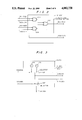
- FIG. 1 illustrates a preferred embodiment of the invention
- FIG. 2 illustrates a detailed composition of clock supply control sections 101 and 201 of FIG. 1;
- FIG. 3 illustrates a detailed composition of clock supplying units 10 and 20 of FIG. 1;
- FIGS. 4 and 5 are diagrams for explaining the operation of the preferred embodiment of the present invention.
- a preferred embodiment of the present invention is provided with a plurality of data processing units 1 and 2 for performing processing operations in accordance with externally supplied clock signals, and a plurality of clock supply units 10 and 20 for varying the mode of clock supply to the data processing units 1 and 2.
- the plural data processing units 1 and 2 respectively have clock control sections 11 and 21 for controlling alterations in the clock supply from the corresponding clock supplying units 10 and 20.
- the clock control sections 11 and 21 have clock supplying unit designating sections 102 and 202 for sending out a signal to designate clock supplying unit 10 or 20, whichever the pertinent data processing unit is to receive clock signals from, to clock supplying unit designating lines 301 and 302; clock switching sections 103 and 203 for generating clock switchover ordering signals on clock switching lines 303 and 304; and clock supply control sections 101 and 201 for outputting, on the basis of signals supplied from the clock supplying unit designating sections 102 and 202 and the clock switching sections 103 and 203 via the lines 301 to 304, clock switching unit switchover ordering signals to lines 305 and 307 and clock switchover ordering signals to lines 306 and 308.
- clock supply control section 101 Since these clock supply control sections 101 and 201 are similarly structured, the following detailed description will be made with reference to clock supply control section 101 alone.
- the clock supply control section 101 is provided with an AND gate 1011 for controlling the switching of clock signals for data processing unit 1 on the basis of a signal given from the clock supplying unit designating section 102 via the line 301 and another signal given from the clock switching section 103 via the line 303; an AND gate 1012 for controlling the switching of clock signals for data processing unit 2 on the basis of a signal inverted from the signal given from the clock supplying unit designating section 202 via the line 302 and another signal given from the clock switching section 203 via the line 304; and an OR gate 1013 for outputting signals from the gates 1011 and 1012 to the line 306, as clock switchover ordering signals for the clock supplying unit 10.
- the clock supply control section 101 outputs the signal given via the line 301 as the clock supplying unit switchover ordering signal to the line 305.
- the clock supplying unit 10 receiving the inputs of signals from this clock supply control section 101 via the lines 305 and 306 is structured similarly to the clock supplying unit 20. Therefore the detailed description hereunder will refer to the clock supplying unit 10 alone.
- the clock supplying unit 10 comprises a first oscillator 104 for generating clock signals at one frequency, a second oscillator 105 for generating clock signals at a different frequency from the first oscillator 104, a selector 106 responsive to the clock switchover ordering signal given from the clock supply control section 101 via the line 306 for selecting either the clock signals from the first oscillator 104 or those from the second oscillator 105, and another selector 107 responsive to the clock supplying unit switchover ordering signal given from the clock supply control unit 101 via the line 305 for selecting the output of the selector 106 via a line 309 or clock signals given from the other clock supplying unit 20 via a line 310 and outputting clock signals to a line 311.
- the clock supplying unit designating section 102 of the data processing unit 1 orders the use of the clock signals from the clock supplying unit 10, and outputs a signal to that effect to the line 301.
- the clock supplying unit designating section 202 of the data processing unit 2 orders the use of the clock signals from the clock supplying unit 10, and outputs a signal to that effect to the line 302.
- the clock supply control section 101 responding to a signal given via the line 301, sends out to the line 305 a signal ordering the supply of clock signals from the clock supplying unit 10.
- the selector 107 of the clock supplying unit 10 selects the output of the selector 106 in response to a signal from the line 305, and supplies it to the data processing unit 1 via the line 311 as the clock signals for its use.
- the clock supply control section 201 responding to a signal given via the line 302, sends out to the line 307 a signal ordering the supply of clock signals from the clock supplying unit 10.
- the selector 107 of the clock supplying unit 20 responding to a signal from the line 307, selects clock signals given from the clock supplying unit 10 via the line 309, and supplies them to the data processing unit 2 by way of a line 312.
- the clock switching section 103 of the data processing unit 1 generates, and sends out to the line 303, a clock switchover ordering signal.
- the gate 1011 of the clock supply control section 101 responding to signals from the lines 301 and 303, generates a clock switching effective signal for the unit it belongs to, transmits the signal via the gate 1013 and the line 306, and supplies it to the clock supplying unit 10 as the clock switchover ordering signal.
- the selector 106 of the clock supplying unit 10 responding to the switchover ordering signal from the line 306, switches over the choice from the output of the first oscillator 104 to that of the second oscillator 105 or vice versa.
- the output of the selector 106 is transmitted via the line 309 to the second clock supplying unit 20 and, at the same time, is supplied to the data processing unit 1 via the selector 107 and the line 311.
- the gate 1012 of the clock supply control section 201 of the data processing unit 2 invalidates the clock switchover ordering signal, given via the line 303, by the negative logic of the unit designating signal given via the line 301. Therefore, the clock supply control section 201 gives no clock switching instruction to the clock supplying unit 20.
- the clock switching section 203 of the data processing unit 2 generates, and sends out to the line 304, a clock switchover ordering signal.
- the gate 1012 of the clock control section 101 of the data processing unit 1 validates the clock switchover ordering signal, given via the line 304, by the negative logic of the unit designating signal given via the line 302.
- the validated signal is given to the clock supplying unit 10 as the switchover ordering signal via the gate 1013 and the line 306.
- the clock supplying unit 10 performs the same clock switching operation as at processing step 410.
- the gate 1011 of the clock control section 201 of the data processing unit 2 invalidates the clock switchover ordering signals, given via the line 304, with the unit designating signal given via the line 302. Therefore, the clock control section 201 gives no clock switchover ordering signal to the clock supplying unit 20.
- a clock switching instruction from either data processing unit, 1 or 2 can switch the clock signals from only the clock supplying unit which currently is supplying clock signals to the processing unit.
- the clock supplying unit switching section 102 of the data processing unit 1 outputs a unit designating signal to the line 301 to receive clock signals from the clock supplying unit 20.
- the clock supplying unit switching section 202 of the data processing unit 2 outputs a unit designating signal to the line 302 to receive clock signals from the clock supplying unit 10.
- the clock control section 101 of the data processing unit 1 supplies the clock supplying unit 10 via the line 305 with the clock supplying unit 20 designating signal given via the line 301 as the signal to order designation of the unit 20.
- the clock control section 201 of the data processing unit 2 supplies the clock supplying unit 20 via the line 307 with the clock supplying unit 10 designating signal given via the line 302 as the signal to order designation of the unit 10.
- the selector 107 of the clock supplying unit 10 selects, and supplies the data processing unit 1 via the line 311 with, the clock signals given from the clock supplying unit 20 via the line 310. Further at processing step 420, the selector 107 of the clock supplying unit 20 selects, and supplies the data processing unit 2 via the line 312 with the clock signals given from the clock supplying unit 10 via the line 309.
- the data processing unit 2 receives clock signals from the clock supplying unit 10. Therefore, when it is desired to change the clock cycle for the data processing unit 2, a clock switching instruction should be given to the clock supplying unit 10 alone. This operation will be described below.
- the clock switching section 103 outputs a clock switchover ordering signal to the line 304.
- the gate 1011 of the clock supply control section 201 invalidates the clock switchover ordering signal, given via the line 304, with the unit designating signal given via the line 302. Therefore, the clock control section 201 gives no clock switchover instruction to the clock supplying unit 20 via the line 308.
- the gate 1012 of the clock supply control section 101 generates from the clock switchover ordering signal, given via the line 304, a clock switchover ordering signal for the clock supply unit 10 by the negative logic of the unit designating signal given via the line 302. This signal is given to the clock supplying unit 10 as the clock switchover ordering signal via the gate 1013 and the line 306.
- the selector 106 of the clock supplying unit 10 responding to the switchover ordering signal given via the line 306, switches over the choice from the output of the first oscillator 104 to that of the second oscillator 105 or vice versa.
- the output of the selector 106 is supplied via the line 309, the second clock supplying unit 20 and the line 312 to the data processing unit 2.
- the system keeps unchanged the state of clock supply even if the clock supplying unit is switched owing to an oscillator trouble or the like in the clock supplying unit, so that the state of clock supply need not be reset. Further the system makes it unnecessary, in switching the clock supply, to be conscious of the relationship between the clock supplying unit and the data processing unit, and only the data processing unit has to be taken account of, resulting in additional improvement of operational efficiency. Moreover, if the clock trains supplied by two clock supplying units are made different from each other unlike in the above described embodiment of the invention wherein they are identical, the variety of clock supply modes will be doubled to provide effective means for failure margin tests of clock signals for early trouble-shooting in system maintenance.
Abstract
Description
Claims (4)
Applications Claiming Priority (2)
| Application Number | Priority Date | Filing Date | Title |
|---|---|---|---|
| JP62-156492 | 1987-06-25 | ||
| JP15649287 | 1987-06-25 |
Publications (1)
| Publication Number | Publication Date |
|---|---|
| US4882738A true US4882738A (en) | 1989-11-21 |
Family
ID=15628937
Family Applications (1)
| Application Number | Title | Priority Date | Filing Date |
|---|---|---|---|
| US07/211,281 Expired - Lifetime US4882738A (en) | 1987-06-25 | 1988-06-24 | Clock control system |
Country Status (1)
| Country | Link |
|---|---|
| US (1) | US4882738A (en) |
Cited By (11)
| Publication number | Priority date | Publication date | Assignee | Title |
|---|---|---|---|---|
| US5057703A (en) * | 1989-08-28 | 1991-10-15 | Siemens Aktiengesellschaft | Working/standby clock pulse supply for digital systems |
| US5089793A (en) * | 1989-10-16 | 1992-02-18 | Seiko Epson Corporation | Semiconductor device having an oscillatory circuit |
| US5289138A (en) * | 1992-07-30 | 1994-02-22 | Amdahl Corportion | Apparatus for synchronously selecting different oscillators as system clock source |
| US5355090A (en) * | 1989-10-06 | 1994-10-11 | Rockwell International Corporation | Phase corrector for redundant clock systems and method |
| US5381542A (en) * | 1991-07-29 | 1995-01-10 | Unisys Corporation | System for switching between a plurality of clock sources upon detection of phase alignment thereof and disabling all other clock sources |
| US5422915A (en) * | 1993-12-23 | 1995-06-06 | Unisys Corporation | Fault tolerant clock distribution system |
| US5452436A (en) * | 1989-08-28 | 1995-09-19 | Hitachi, Ltd. | System for connecting plurality of electronic units to data and clock buses wherein transmitting and receiving data in synchronization with transmitting and receiving clock signals |
| US5574753A (en) * | 1993-12-23 | 1996-11-12 | Unisys Corporation | Glitch free clock start/stop control circuit for outputting a single clock signal and a single sync signal from a plurality of sync signal inputs and a plurality of clock signal inputs |
| US5594895A (en) * | 1992-12-15 | 1997-01-14 | International Business Machines Corporation | Method and apparatus for switching between clock generators only when activity on a bus can be stopped |
| US6477659B1 (en) * | 1999-09-03 | 2002-11-05 | Sun Microsystems, Inc. | Measuring timing margins in digital systems by varying a programmable clock skew |
| US20060072679A1 (en) * | 2004-10-01 | 2006-04-06 | Ching-Yung Chen | Method and device for modulation recognition of digitally modulated signals with multi-level magnitudes |
Citations (6)
| Publication number | Priority date | Publication date | Assignee | Title |
|---|---|---|---|---|
| US4229699A (en) * | 1978-05-22 | 1980-10-21 | Data General Corporation | Multiple clock selection system |
| US4254492A (en) * | 1979-04-02 | 1981-03-03 | Rockwell International Corporation | Redundant clock system utilizing nonsynchronous oscillators |
| US4322580A (en) * | 1980-09-02 | 1982-03-30 | Gte Automatic Electric Labs Inc. | Clock selection circuit |
| US4480198A (en) * | 1981-05-20 | 1984-10-30 | La Telephonie Industrielle Et Commerciale Telic Alcatel | Device for increasing the operational security of a duplicated clock |
| US4564943A (en) * | 1983-07-05 | 1986-01-14 | International Business Machines | System path stressing |
| US4574377A (en) * | 1982-11-26 | 1986-03-04 | Fujitsu Limited | Synchronization method and apparatus in redundant time-division-multiple-access communication equipment |
-
1988
- 1988-06-24 US US07/211,281 patent/US4882738A/en not_active Expired - Lifetime
Patent Citations (6)
| Publication number | Priority date | Publication date | Assignee | Title |
|---|---|---|---|---|
| US4229699A (en) * | 1978-05-22 | 1980-10-21 | Data General Corporation | Multiple clock selection system |
| US4254492A (en) * | 1979-04-02 | 1981-03-03 | Rockwell International Corporation | Redundant clock system utilizing nonsynchronous oscillators |
| US4322580A (en) * | 1980-09-02 | 1982-03-30 | Gte Automatic Electric Labs Inc. | Clock selection circuit |
| US4480198A (en) * | 1981-05-20 | 1984-10-30 | La Telephonie Industrielle Et Commerciale Telic Alcatel | Device for increasing the operational security of a duplicated clock |
| US4574377A (en) * | 1982-11-26 | 1986-03-04 | Fujitsu Limited | Synchronization method and apparatus in redundant time-division-multiple-access communication equipment |
| US4564943A (en) * | 1983-07-05 | 1986-01-14 | International Business Machines | System path stressing |
Cited By (13)
| Publication number | Priority date | Publication date | Assignee | Title |
|---|---|---|---|---|
| US5057703A (en) * | 1989-08-28 | 1991-10-15 | Siemens Aktiengesellschaft | Working/standby clock pulse supply for digital systems |
| US5452436A (en) * | 1989-08-28 | 1995-09-19 | Hitachi, Ltd. | System for connecting plurality of electronic units to data and clock buses wherein transmitting and receiving data in synchronization with transmitting and receiving clock signals |
| US5355090A (en) * | 1989-10-06 | 1994-10-11 | Rockwell International Corporation | Phase corrector for redundant clock systems and method |
| US5089793A (en) * | 1989-10-16 | 1992-02-18 | Seiko Epson Corporation | Semiconductor device having an oscillatory circuit |
| US5381542A (en) * | 1991-07-29 | 1995-01-10 | Unisys Corporation | System for switching between a plurality of clock sources upon detection of phase alignment thereof and disabling all other clock sources |
| US5467466A (en) * | 1991-07-29 | 1995-11-14 | Unisys Corporation | Method for switching between a plurality of clock sources upon detection of phase alignment thereof and disabling all other clock sources |
| US5289138A (en) * | 1992-07-30 | 1994-02-22 | Amdahl Corportion | Apparatus for synchronously selecting different oscillators as system clock source |
| US5594895A (en) * | 1992-12-15 | 1997-01-14 | International Business Machines Corporation | Method and apparatus for switching between clock generators only when activity on a bus can be stopped |
| US5422915A (en) * | 1993-12-23 | 1995-06-06 | Unisys Corporation | Fault tolerant clock distribution system |
| US5574753A (en) * | 1993-12-23 | 1996-11-12 | Unisys Corporation | Glitch free clock start/stop control circuit for outputting a single clock signal and a single sync signal from a plurality of sync signal inputs and a plurality of clock signal inputs |
| US6477659B1 (en) * | 1999-09-03 | 2002-11-05 | Sun Microsystems, Inc. | Measuring timing margins in digital systems by varying a programmable clock skew |
| US20060072679A1 (en) * | 2004-10-01 | 2006-04-06 | Ching-Yung Chen | Method and device for modulation recognition of digitally modulated signals with multi-level magnitudes |
| US7379507B2 (en) * | 2004-10-01 | 2008-05-27 | Industrial Technology Research Institute | Method and device for modulation recognition of digitally modulated signals with multi-level magnitudes |
Similar Documents
| Publication | Publication Date | Title |
|---|---|---|
| US4245342A (en) | One-for-n modem control apparatus | |
| US4095267A (en) | Clock pulse control system for microcomputer systems | |
| US4882738A (en) | Clock control system | |
| US4208715A (en) | Dual data processing system | |
| US3594656A (en) | Automatic clock frequency-switching system | |
| JP2000002754A (en) | Scan flip-flop circuit | |
| US5357491A (en) | Clock selection control device | |
| US5502819A (en) | Clock distribution system for reducing clock skew between processors in a dual sided tightly coupled system | |
| JPS63175913A (en) | Clock supplying system | |
| US5230046A (en) | System for independently controlling supply of a clock signal to a selected group of the arithmetic processors connected in series | |
| CN1302121A (en) | Clock signal switching and selecting method in synchronous clock supply system and its device | |
| JPH04287458A (en) | Transmission rate control system for serial interface | |
| JP2665070B2 (en) | Bus circuit | |
| JPH07281918A (en) | Switching circuit for duplex signal relay system | |
| JPS59231668A (en) | Dual clock signal switching system | |
| JPS58222328A (en) | Channel switch device | |
| JP2737916B2 (en) | Digital signal connection device | |
| JPH0797771B2 (en) | Clock control system | |
| JPH05183971A (en) | System clock device | |
| JPS57117043A (en) | Digital operation control device | |
| JPS6145266B2 (en) | ||
| JPH05165681A (en) | State history device | |
| JPH03210482A (en) | Apparatus for stopping unnecessary function | |
| JPH03109827A (en) | Signal selecting system in duplexing constitution equipment | |
| JPS6251013B2 (en) |
Legal Events
| Date | Code | Title | Description |
|---|---|---|---|
| AS | Assignment |
Owner name: NEC CORPORATION, 33-1, SHIBA 5-CHOME, MINATO-KU, T Free format text: ASSIGNMENT OF ASSIGNORS INTEREST.;ASSIGNOR:SUZUKI, TAKASHI;REEL/FRAME:004935/0410 Effective date: 19880616 |
|
| STCF | Information on status: patent grant |
Free format text: PATENTED CASE |
|
| FPAY | Fee payment |
Year of fee payment: 4 |
|
| REMI | Maintenance fee reminder mailed | ||
| FEPP | Fee payment procedure |
Free format text: PAYOR NUMBER ASSIGNED (ORIGINAL EVENT CODE: ASPN); ENTITY STATUS OF PATENT OWNER: LARGE ENTITY |
|
| FEPP | Fee payment procedure |
Free format text: PAYOR NUMBER ASSIGNED (ORIGINAL EVENT CODE: ASPN); ENTITY STATUS OF PATENT OWNER: LARGE ENTITY Free format text: PAYER NUMBER DE-ASSIGNED (ORIGINAL EVENT CODE: RMPN); ENTITY STATUS OF PATENT OWNER: LARGE ENTITY |
|
| FPAY | Fee payment |
Year of fee payment: 8 |
|
| FEPP | Fee payment procedure |
Free format text: PAYER NUMBER DE-ASSIGNED (ORIGINAL EVENT CODE: RMPN); ENTITY STATUS OF PATENT OWNER: LARGE ENTITY |
|
| FEPP | Fee payment procedure |
Free format text: PAYOR NUMBER ASSIGNED (ORIGINAL EVENT CODE: ASPN); ENTITY STATUS OF PATENT OWNER: LARGE ENTITY |
|
| FPAY | Fee payment |
Year of fee payment: 12 |