US4900276A - Electrical connector with pin retention feature - Google Patents
Electrical connector with pin retention feature Download PDFInfo
- Publication number
- US4900276A US4900276A US07/378,544 US37854489A US4900276A US 4900276 A US4900276 A US 4900276A US 37854489 A US37854489 A US 37854489A US 4900276 A US4900276 A US 4900276A
- Authority
- US
- United States
- Prior art keywords
- pins
- pair
- crimp
- header
- electrical connector
- Prior art date
- Legal status (The legal status is an assumption and is not a legal conclusion. Google has not performed a legal analysis and makes no representation as to the accuracy of the status listed.)
- Expired - Lifetime
Links
Images


Classifications
-
- H—ELECTRICITY
- H01—ELECTRIC ELEMENTS
- H01R—ELECTRICALLY-CONDUCTIVE CONNECTIONS; STRUCTURAL ASSOCIATIONS OF A PLURALITY OF MUTUALLY-INSULATED ELECTRICAL CONNECTING ELEMENTS; COUPLING DEVICES; CURRENT COLLECTORS
- H01R12/00—Structural associations of a plurality of mutually-insulated electrical connecting elements, specially adapted for printed circuits, e.g. printed circuit boards [PCB], flat or ribbon cables, or like generally planar structures, e.g. terminal strips, terminal blocks; Coupling devices specially adapted for printed circuits, flat or ribbon cables, or like generally planar structures; Terminals specially adapted for contact with, or insertion into, printed circuits, flat or ribbon cables, or like generally planar structures
- H01R12/50—Fixed connections
- H01R12/51—Fixed connections for rigid printed circuits or like structures
- H01R12/55—Fixed connections for rigid printed circuits or like structures characterised by the terminals
- H01R12/58—Fixed connections for rigid printed circuits or like structures characterised by the terminals terminals for insertion into holes
-
- H—ELECTRICITY
- H05—ELECTRIC TECHNIQUES NOT OTHERWISE PROVIDED FOR
- H05K—PRINTED CIRCUITS; CASINGS OR CONSTRUCTIONAL DETAILS OF ELECTRIC APPARATUS; MANUFACTURE OF ASSEMBLAGES OF ELECTRICAL COMPONENTS
- H05K3/00—Apparatus or processes for manufacturing printed circuits
- H05K3/30—Assembling printed circuits with electric components, e.g. with resistor
- H05K3/306—Lead-in-hole components, e.g. affixing or retention before soldering, spacing means
- H05K3/308—Adaptations of leads
-
- H—ELECTRICITY
- H05—ELECTRIC TECHNIQUES NOT OTHERWISE PROVIDED FOR
- H05K—PRINTED CIRCUITS; CASINGS OR CONSTRUCTIONAL DETAILS OF ELECTRIC APPARATUS; MANUFACTURE OF ASSEMBLAGES OF ELECTRICAL COMPONENTS
- H05K2201/00—Indexing scheme relating to printed circuits covered by H05K1/00
- H05K2201/10—Details of components or other objects attached to or integrated in a printed circuit board
- H05K2201/10007—Types of components
- H05K2201/10189—Non-printed connector
-
- H—ELECTRICITY
- H05—ELECTRIC TECHNIQUES NOT OTHERWISE PROVIDED FOR
- H05K—PRINTED CIRCUITS; CASINGS OR CONSTRUCTIONAL DETAILS OF ELECTRIC APPARATUS; MANUFACTURE OF ASSEMBLAGES OF ELECTRICAL COMPONENTS
- H05K2201/00—Indexing scheme relating to printed circuits covered by H05K1/00
- H05K2201/10—Details of components or other objects attached to or integrated in a printed circuit board
- H05K2201/10613—Details of electrical connections of non-printed components, e.g. special leads
- H05K2201/10742—Details of leads
- H05K2201/1075—Shape details
- H05K2201/10757—Bent leads
-
- H—ELECTRICITY
- H05—ELECTRIC TECHNIQUES NOT OTHERWISE PROVIDED FOR
- H05K—PRINTED CIRCUITS; CASINGS OR CONSTRUCTIONAL DETAILS OF ELECTRIC APPARATUS; MANUFACTURE OF ASSEMBLAGES OF ELECTRICAL COMPONENTS
- H05K2201/00—Indexing scheme relating to printed circuits covered by H05K1/00
- H05K2201/10—Details of components or other objects attached to or integrated in a printed circuit board
- H05K2201/10613—Details of electrical connections of non-printed components, e.g. special leads
- H05K2201/10742—Details of leads
- H05K2201/1075—Shape details
- H05K2201/10878—Means for retention of a lead in a hole
Definitions
- This invention relates to electrical connectors affixed to printed circuit boards and, more particularly, to providing retaining means for such connectors while its terminal pins are soldered to the printed curcuit board.
- Retention during soldering is particularly important in connection with the more recent multi-terminal connectors.
- connectors have flat, thin leads, which can be readily crimped as in the discrete components of the past, the retention is not a serious problem.
- the easily crimped flat, thin leads usually have a large offset permitting adequate room to pass through the board holes.
- the crimped portion passes completely through holes and locks to the other end of the holes.
- the thickness of the board and location are critical.
- headers include numerous male terminal pins surrounded by various plastics.
- the male pins are typically square metal posts approximately 0.025 inches square and are very stiff. Because of the size and stiffness of such square male pins, headers are soldered to printed circuit utilizing various hold-down devices to retain the header in place during the soldering operation. Such devices include mechanical fasteners such as bolts and screws. Weighted plates are also used. These are placed atop the headers and removed after the soldering process. Although such methods work, they are expensive because they are labor intensive.
- Robotic loaders typically have an upper limit on insertion forces (for example, about 15 pounds) to protect the circuit board in case of a misplaced or damaged component. As this load limit is reached, the insertion head of the robotic loader retracts to provide this safety feature. Consequently, retention features must have relatively low insertion forces to be used with robotic loaders.
- the present invention provides a solution for retaining an electrical connector header in the correct position during soldering and other handling operations.
- the terminal end of one or more pairs of male pins are deformed or crimped in such a manner that they operate in conjunction with one or more pairs of printed circuit board holes to retain the entire header in the correct position during soldering.
- each pair of deformed pins provide very high normal forces against the inside of the corresponding pair of opposing printed circuit board holes into which the pins are inserted.
- location of the crimp is not dependent upon thickness of the printed circuit board because retention depends upon the complementary normal forces of a pair of pins against two opposing printed circuit board holes.
- the complementary action of each pin of the pair against the corresponding surface of the hole provides retention, no matter whether the board is relatively thin or thick.
- the thick pins allow for very little room for offset without creating very high insertion forces.
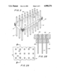
- FIG. 1 is a perspective view of a first embodiment of the present invention illustrating a pair of crimped retaining pins in a double row vertical header.
- FIG. 1A is a top view of FIG. 1.
- FIG. 1B is a sectional view taken along the line B--B of FIG. 1A, after insertion in a printed circuit board.
- FIGS. 2, 2A and 2B are respectively similarly views of a second embodiment of the present invention illustrating a pair of crimped retaining pins in a triple row vertical header.
- FIGS. 3, 3A, 3B, and 3C are also respectively similar views of a third embodiment of the present invention illustrating two pairs of crimped retaining pins in a single row vertical header.
- FIGS. 4, 4A, and 4B are also respectively similar views of two pairs of crimped pins in a single row, right angle header.
- FIGS. 5, 5A and 5B are also respectively similar views of a pair of crimped retaining pins in a double row, right angle header.
- FIG. 1 illustrates a first embodiment of the present invention wherein a double row vertical header 10 is shown.
- the header comprises two rows of square male terminal pins 12.
- Such male terminal pins are an industry standard 0.025 inches square.
- the pins are held in a plastic retainer or wafer 14.
- a pair of adjoining pins, 12A and 12B have been crimped as shown at their terminal or insertion end.
- the deformation is such that the crimped portions of pins 12A and 12B extend toward each other.
- the retention feature of the present invention will work equally well if the crimped portions both extend away from each other. What is important is that each crimped portion of the pair cooperate against corresponding surfaces in the printed circuit board holes, as explained below.
- Buttons 16 are provided on the wafer 14 to provide an offset between wafer and printed circuit board after insertion of the header 10. This allows for adequate cleaning after the soldering operation.
- FIG. 1B illustrates the retention action of the pair of crimped pins 12A and 12B after the header 10 is inserted into a printed circuit board 18.
- the crimped end of the pins are shown within the holes of the board. It should be noted that retention can be achieved by contact of the crimped portion of each lead with only one side of its hole at points identified as 19A and 19B, respectively.
- the normal forces exerted against hole surfaces 19A and 19B by the crimped portion of pins 12A and 12B is sufficiently high to provide the necessary retention during the soldering operation.
- the thickness of the printed circuit board is not as critical as where retention due to a terminal or lead deformation requires contact with opposite sides of the same to circuit board hole.
- the present invention operates equally well in very thin and very thick printed circuit boards. What is important is that at least a pair of complementary pins be similarly crimped so that normal forces of the crimped portion of each act cooperatively against the corresponding surface of each respective printed circuit board hole.
- FIGS. 2, 2A and 2B illustrate a second embodiment of the present invention where like parts are identified by the same reference number.
- This second embodiment shows a triple row vertical header 20 differing from header 10 essentially only in that it contains three instead of two rows of pins 12.
- a single pair of crimped terminals 12A and 12B is utilized here also, one from the first and third rows. They are separated by a regular pin 12.
- the retention action in the printed circuit board 18 is otherwise identical as shown in FIG. 2B.
- FIGS. 3, 3A and 3B illustrate a third embodiment of the present invention.
- the header 30 in the embodiment comprises but a single row of pins held in a plastic wafer 34 similar to 14 of the prior embodiments.
- pairs 32A and 32B cooperate with one another as do pairs 32C and 32D in a manner similar to the single pair of crimped pins in the first two embodiments to provide retention of the header in the printed circuit board.
- complementary crimped terminals 32A (shown in solid) and 32B (shown in phantom) have their crimped portion exerting normal forces against opposite surfaces of their respective printed circuit board holes, thereby achieving the same retention action as in the prior embodiments.
- crimped terminals 32C (solid) and 32C (phantom) shown in FIG. 3D are examples of the same.
- FIGS. 4, 4A and 4B illustrate a fourth embodiment of the present invention.
- the header 40 is also a single row header but the terminal pins 42 are bent at right angles at one end. This is because header 40 is designed to be inserted into printed circuit board 48 at right angles as shown in FIG. 4C. As before, the pins 42 are held by a plastic wafer 44. Header 40 also has two pairs of pins crimped alternatively as in the header of FIG. 3. The crimps are at the right angle portion of the pins for obvious reasons. Thus, as in the case of the embodiment of FIG. 3, pairs 42A and 42B and pairs 42C and 42D of crimped terminals cooperate to retain the header in the printed circuit board 48.
- FIG. 4B illustrates the previously explained cooperative retaining action between crimped pin 42B (solid) and 42A (phantom). The same occurs in the case of pins 42C and 42D. Again, adequate retention can be obtained with a single pair of crimped pins.
- FIGS. 5, 5A and 5B illustrate a fifth embodiment of the present invention.
- the headers 50 is a double row, right angle header, meaning that is comprises a double row of pins 52 held by a wafer 54 where all the pins are set at right angles for insertion into a printed circuit board.
- a pair of pins 52A and 52B are crimped in the manner previously described.
- crimped terminals cooperate as did crimped pins 12A and 12B ion the embodiment of FIG. 1 to retain header 50 in the proper position during soldering.
Landscapes
- Engineering & Computer Science (AREA)
- Manufacturing & Machinery (AREA)
- Microelectronics & Electronic Packaging (AREA)
- Coupling Device And Connection With Printed Circuit (AREA)
Abstract
Description
Claims (20)
Priority Applications (1)
| Application Number | Priority Date | Filing Date | Title |
|---|---|---|---|
| US07/378,544 US4900276A (en) | 1986-03-05 | 1989-07-11 | Electrical connector with pin retention feature |
Applications Claiming Priority (3)
| Application Number | Priority Date | Filing Date | Title |
|---|---|---|---|
| US83653486A | 1986-03-05 | 1986-03-05 | |
| US07053550 US4847588B1 (en) | 1986-03-05 | 1987-05-26 | Electrical connector with pin retention feature |
| US07/378,544 US4900276A (en) | 1986-03-05 | 1989-07-11 | Electrical connector with pin retention feature |
Related Parent Applications (1)
| Application Number | Title | Priority Date | Filing Date |
|---|---|---|---|
| US07053550 Continuation US4847588B1 (en) | 1986-03-05 | 1987-05-26 | Electrical connector with pin retention feature |
Publications (1)
| Publication Number | Publication Date |
|---|---|
| US4900276A true US4900276A (en) | 1990-02-13 |
Family
ID=27368444
Family Applications (1)
| Application Number | Title | Priority Date | Filing Date |
|---|---|---|---|
| US07/378,544 Expired - Lifetime US4900276A (en) | 1986-03-05 | 1989-07-11 | Electrical connector with pin retention feature |
Country Status (1)
| Country | Link |
|---|---|
| US (1) | US4900276A (en) |
Cited By (18)
| Publication number | Priority date | Publication date | Assignee | Title |
|---|---|---|---|---|
| WO1992020203A1 (en) * | 1991-05-08 | 1992-11-12 | General Datacomm, Inc. | Integrated circuit packages using tapered spring contact leads for direct mounting to circuit boards |
| US5199907A (en) * | 1992-06-18 | 1993-04-06 | Amp Incorporated | Electrical connector having contacts with board retention feature |
| US5232379A (en) * | 1992-02-28 | 1993-08-03 | Foxconn International, Inc. | Connector with mounting means for SMT |
| US5257941A (en) * | 1991-08-15 | 1993-11-02 | E. I. Du Pont De Nemours And Company | Connector and electrical connection structure using the same |
| US5411404A (en) * | 1993-10-29 | 1995-05-02 | The Whitaker Corporation | Electrical connector having bus bars providing circuit board retention |
| US5498174A (en) * | 1994-10-18 | 1996-03-12 | The Whitaker Corporation | Electrical connector with spring leg retention feature |
| US6035529A (en) * | 1997-11-25 | 2000-03-14 | Micron Electronics, Inc. | Header pin pre-loaded method |
| US6216338B1 (en) | 1997-11-25 | 2001-04-17 | Micron Electronics, Inc. | Header pin pre-load apparatus |
| US6371802B1 (en) * | 2000-11-21 | 2002-04-16 | Hon Hai Precision Ind. Co., Ltd. | Header connector with stabilizer |
| US20040097141A1 (en) * | 2002-07-30 | 2004-05-20 | Yakov Belopolsky | Electrical connector and contact for use therein |
| US20040120125A1 (en) * | 2002-12-19 | 2004-06-24 | Tillman Frazier Taylor | Retention system for retaining assemblies within an electronic device chassis |
| US20040166706A1 (en) * | 2003-02-20 | 2004-08-26 | Xu Pei Ren | SMT-compatible through-hole electrical connector |
| US6857911B2 (en) * | 2001-03-23 | 2005-02-22 | Yazaki Corporation | Common-use connector for multiple purpose and method of manufacturing the connector |
| US7540744B1 (en) * | 2008-01-08 | 2009-06-02 | Fci Americas Technology, Inc. | Shared hole orthogonal footprint with backdrilled vias |
| US9819106B2 (en) * | 2014-10-02 | 2017-11-14 | Wago Verwaltungsgesellschaft Mbh | Male strip connector |
| US20190090392A1 (en) * | 2017-09-15 | 2019-03-21 | Dell Products, L.P. | Reducing displacement of selected components during printed circuit board assembly (pcba) manufacturing |
| US11083293B2 (en) * | 2019-10-17 | 2021-08-10 | Clark Davis | Modular stackable shelves |
| US11767867B2 (en) | 2020-11-17 | 2023-09-26 | Clark Davis | Pivoting joint for wooden furniture |
Citations (15)
| Publication number | Priority date | Publication date | Assignee | Title |
|---|---|---|---|---|
| US2754486A (en) * | 1953-10-20 | 1956-07-10 | Stackpole Carbon Co | Printed circuit electrical component |
| US2958063A (en) * | 1955-07-12 | 1960-10-25 | Stanwyck Edmund | Terminal for coil support |
| US3056939A (en) * | 1960-07-26 | 1962-10-02 | Illinois Tool Works | Component lead-locking arrangement |
| US3162721A (en) * | 1960-07-26 | 1964-12-22 | Illinois Tool Works | Component lead-locking arrangement |
| US3239720A (en) * | 1964-04-21 | 1966-03-08 | Illinois Tool Works | Capacitor construction and mounting thereof |
| DE1816073A1 (en) * | 1968-12-20 | 1970-07-02 | Siemens Ag | Electrical component intended for connection to a circuit board |
| US3524108A (en) * | 1967-12-26 | 1970-08-11 | Cts Corp | Board mounted modular circuit component and improvement therein |
| DE1916410A1 (en) * | 1969-03-31 | 1970-10-08 | Siemens Ag | Electrical component with resilient connection conductors |
| US3747045A (en) * | 1971-04-19 | 1973-07-17 | Sprague Electric Co | Lead locking configuration for electrical components |
| FR2221829A1 (en) * | 1973-03-16 | 1974-10-11 | Meyer Jean | Fixing device for conductor on insulated support - consists of single metal stamping press fitted into support |
| DE2742716A1 (en) * | 1977-09-22 | 1979-04-05 | Siemens Ag | Connection between electrical component and printed circuit board - by folding wires back to form radially-acting spring contacts to through plated hole |
| US4407556A (en) * | 1981-09-21 | 1983-10-04 | Teletype Corporation | Retaining clip for an electrical connector |
| JPS60164342A (en) * | 1984-02-07 | 1985-08-27 | Nec Corp | Electronic part socket for printed board |
| US4553801A (en) * | 1982-09-23 | 1985-11-19 | Panduit Corp. | Locking and polarizing header |
| US4735587A (en) * | 1986-02-12 | 1988-04-05 | Specialty Electronics, Inc. | Pin header with board retention tail |
-
1989
- 1989-07-11 US US07/378,544 patent/US4900276A/en not_active Expired - Lifetime
Patent Citations (15)
| Publication number | Priority date | Publication date | Assignee | Title |
|---|---|---|---|---|
| US2754486A (en) * | 1953-10-20 | 1956-07-10 | Stackpole Carbon Co | Printed circuit electrical component |
| US2958063A (en) * | 1955-07-12 | 1960-10-25 | Stanwyck Edmund | Terminal for coil support |
| US3056939A (en) * | 1960-07-26 | 1962-10-02 | Illinois Tool Works | Component lead-locking arrangement |
| US3162721A (en) * | 1960-07-26 | 1964-12-22 | Illinois Tool Works | Component lead-locking arrangement |
| US3239720A (en) * | 1964-04-21 | 1966-03-08 | Illinois Tool Works | Capacitor construction and mounting thereof |
| US3524108A (en) * | 1967-12-26 | 1970-08-11 | Cts Corp | Board mounted modular circuit component and improvement therein |
| DE1816073A1 (en) * | 1968-12-20 | 1970-07-02 | Siemens Ag | Electrical component intended for connection to a circuit board |
| DE1916410A1 (en) * | 1969-03-31 | 1970-10-08 | Siemens Ag | Electrical component with resilient connection conductors |
| US3747045A (en) * | 1971-04-19 | 1973-07-17 | Sprague Electric Co | Lead locking configuration for electrical components |
| FR2221829A1 (en) * | 1973-03-16 | 1974-10-11 | Meyer Jean | Fixing device for conductor on insulated support - consists of single metal stamping press fitted into support |
| DE2742716A1 (en) * | 1977-09-22 | 1979-04-05 | Siemens Ag | Connection between electrical component and printed circuit board - by folding wires back to form radially-acting spring contacts to through plated hole |
| US4407556A (en) * | 1981-09-21 | 1983-10-04 | Teletype Corporation | Retaining clip for an electrical connector |
| US4553801A (en) * | 1982-09-23 | 1985-11-19 | Panduit Corp. | Locking and polarizing header |
| JPS60164342A (en) * | 1984-02-07 | 1985-08-27 | Nec Corp | Electronic part socket for printed board |
| US4735587A (en) * | 1986-02-12 | 1988-04-05 | Specialty Electronics, Inc. | Pin header with board retention tail |
Non-Patent Citations (10)
| Title |
|---|
| AMP Engineering and Purchasing Guide, Fifth Edition, Copyright 1984, pp. I 3 I 14. * |
| AMP Engineering and Purchasing Guide, Fifth Edition, Copyright 1984, pp. I-3-I-14. |
| AMP Standard Products Catalog, Fourth Edition, Issued Mar. 1985, pp. 746 753. * |
| AMP Standard Products Catalog, Fourth Edition, Issued Mar. 1985, pp. 746-753. |
| AMP Standard Products Catalog, Third Edition, Issued Aug. 1983, pp. 693 697. * |
| AMP Standard Products Catalog, Third Edition, Issued Aug. 1983, pp. 693-697. |
| Electronic Design, vol. 33, No. 6, Mar. 1985, pp. 142 150, Hasbrouch Heights, New Jersey, US; J. Sherett Special Edition Report, Connectors . * |
| Electronic Design, vol. 33, No. 6, Mar. 1985, pp. 142-150, Hasbrouch Heights, New Jersey, US; J. Sherett "Special Edition Report, Connectors". |
| Patent Abstracts of Japan, vol. 9, No. 332 (E 370) (2055) 26th Dec. 1985; & JP A 60 164 342 (Nippon Denki) 27 08 1985. * |
| Patent Abstracts of Japan, vol. 9, No. 332 (E-370) (2055) 26th Dec. 1985; & JP-A-60 164 342 (Nippon Denki) 27-08-1985. |
Cited By (23)
| Publication number | Priority date | Publication date | Assignee | Title |
|---|---|---|---|---|
| WO1992020203A1 (en) * | 1991-05-08 | 1992-11-12 | General Datacomm, Inc. | Integrated circuit packages using tapered spring contact leads for direct mounting to circuit boards |
| US5257941A (en) * | 1991-08-15 | 1993-11-02 | E. I. Du Pont De Nemours And Company | Connector and electrical connection structure using the same |
| US5232379A (en) * | 1992-02-28 | 1993-08-03 | Foxconn International, Inc. | Connector with mounting means for SMT |
| US5199907A (en) * | 1992-06-18 | 1993-04-06 | Amp Incorporated | Electrical connector having contacts with board retention feature |
| EP0575092A1 (en) * | 1992-06-18 | 1993-12-22 | The Whitaker Corporation | Electrical connector having contacts with board retention feature |
| US5411404A (en) * | 1993-10-29 | 1995-05-02 | The Whitaker Corporation | Electrical connector having bus bars providing circuit board retention |
| US5462444A (en) * | 1993-10-29 | 1995-10-31 | The Whitaker Corporation | Electrical connector having bus bars providing circuit board retention |
| US5498174A (en) * | 1994-10-18 | 1996-03-12 | The Whitaker Corporation | Electrical connector with spring leg retention feature |
| US6035529A (en) * | 1997-11-25 | 2000-03-14 | Micron Electronics, Inc. | Header pin pre-loaded method |
| US6216338B1 (en) | 1997-11-25 | 2001-04-17 | Micron Electronics, Inc. | Header pin pre-load apparatus |
| US6371802B1 (en) * | 2000-11-21 | 2002-04-16 | Hon Hai Precision Ind. Co., Ltd. | Header connector with stabilizer |
| US6857911B2 (en) * | 2001-03-23 | 2005-02-22 | Yazaki Corporation | Common-use connector for multiple purpose and method of manufacturing the connector |
| US20040097141A1 (en) * | 2002-07-30 | 2004-05-20 | Yakov Belopolsky | Electrical connector and contact for use therein |
| US6974337B2 (en) | 2002-07-30 | 2005-12-13 | Fci Americas Technology, Inc. | Electrical connector and contact for use therein |
| US20040120125A1 (en) * | 2002-12-19 | 2004-06-24 | Tillman Frazier Taylor | Retention system for retaining assemblies within an electronic device chassis |
| US6974914B2 (en) | 2002-12-19 | 2005-12-13 | Hewlett-Packard Development Company, L.P. | Retention system for retaining assemblies within an electric device chassis |
| US20040166706A1 (en) * | 2003-02-20 | 2004-08-26 | Xu Pei Ren | SMT-compatible through-hole electrical connector |
| US7540744B1 (en) * | 2008-01-08 | 2009-06-02 | Fci Americas Technology, Inc. | Shared hole orthogonal footprint with backdrilled vias |
| US9819106B2 (en) * | 2014-10-02 | 2017-11-14 | Wago Verwaltungsgesellschaft Mbh | Male strip connector |
| US20190090392A1 (en) * | 2017-09-15 | 2019-03-21 | Dell Products, L.P. | Reducing displacement of selected components during printed circuit board assembly (pcba) manufacturing |
| US10750647B2 (en) * | 2017-09-15 | 2020-08-18 | Dell Products, L.P. | Reducing displacement of selected components during printed circuit board assembly (PCBA) manufacturing |
| US11083293B2 (en) * | 2019-10-17 | 2021-08-10 | Clark Davis | Modular stackable shelves |
| US11767867B2 (en) | 2020-11-17 | 2023-09-26 | Clark Davis | Pivoting joint for wooden furniture |
Similar Documents
| Publication | Publication Date | Title |
|---|---|---|
| US4847588A (en) | Electrical connector with pin retention feature | |
| US4900276A (en) | Electrical connector with pin retention feature | |
| US5139446A (en) | Electrical connector assembly | |
| US6042389A (en) | Low profile connector | |
| US6241535B1 (en) | Low profile connector | |
| EP0384580B1 (en) | Surface mount HDI contact | |
| EP0543278B1 (en) | Low profile electrical connector | |
| US20040157477A1 (en) | High density connector | |
| EP0204504A2 (en) | Electric connector | |
| EP0499378A2 (en) | Low profile cam-in simm socket | |
| US4018494A (en) | Interconnection for electrically connecting two vertically stacked electronic packages | |
| US4075759A (en) | Transverse connector assembly method | |
| US4726777A (en) | Socket for zig-zag inline package | |
| US3467944A (en) | Interconnection system with precision terminal alignment | |
| US5507653A (en) | Insulative wafers for interconnecting a vertical receptacle to a printed circuit board | |
| US5131872A (en) | Contact spring socket | |
| EP0280508B1 (en) | Through-board electrical component header having integral solder mask | |
| EP0546673B1 (en) | Connector with retention feature | |
| US5022862A (en) | Modular connector | |
| JP2000511328A (en) | Vacuum pickup cap used for handling the receptacle | |
| US5569054A (en) | Electrical connector | |
| US4743081A (en) | Contact element | |
| EP0891124A2 (en) | Three-dimensional electrical interconnection system | |
| JPS62150675A (en) | Pin header | |
| EP0077606B1 (en) | Low or zero insertion force connector for multi-pin arrays |
Legal Events
| Date | Code | Title | Description |
|---|---|---|---|
| STCF | Information on status: patent grant |
Free format text: PATENTED CASE |
|
| AS | Assignment |
Owner name: CHEMICAL BANK, NEW YORK Free format text: SECURITY INTEREST;ASSIGNOR:BERG TECHNOLOGY, INC.;REEL/FRAME:006497/0231 Effective date: 19930226 |
|
| FPAY | Fee payment |
Year of fee payment: 4 |
|
| AS | Assignment |
Owner name: BERG TECHNOLOGY, INC., NEVADA Free format text: ASSIGNMENT OF ASSIGNORS INTEREST;ASSIGNOR:E.I. DU PONT DE NEMOURS AND COMPANY;REEL/FRAME:008321/0185 Effective date: 19961209 |
|
| FPAY | Fee payment |
Year of fee payment: 8 |
|
| FPAY | Fee payment |
Year of fee payment: 12 |