US4901205A - Housing for electronic components - Google Patents
Housing for electronic components Download PDFInfo
- Publication number
- US4901205A US4901205A US07/239,818 US23981888A US4901205A US 4901205 A US4901205 A US 4901205A US 23981888 A US23981888 A US 23981888A US 4901205 A US4901205 A US 4901205A
- Authority
- US
- United States
- Prior art keywords
- housing
- housing member
- electronic components
- circuit board
- board
- Prior art date
- Legal status (The legal status is an assumption and is not a legal conclusion. Google has not performed a legal analysis and makes no representation as to the accuracy of the status listed.)
- Expired - Lifetime
Links
Images

Classifications
-
- G—PHYSICS
- G06—COMPUTING; CALCULATING OR COUNTING
- G06F—ELECTRIC DIGITAL DATA PROCESSING
- G06F1/00—Details not covered by groups G06F3/00 - G06F13/00 and G06F21/00
- G06F1/16—Constructional details or arrangements
- G06F1/18—Packaging or power distribution
- G06F1/183—Internal mounting support structures, e.g. for printed circuit boards, internal connecting means
- G06F1/185—Mounting of expansion boards
-
- G—PHYSICS
- G06—COMPUTING; CALCULATING OR COUNTING
- G06F—ELECTRIC DIGITAL DATA PROCESSING
- G06F1/00—Details not covered by groups G06F3/00 - G06F13/00 and G06F21/00
- G06F1/16—Constructional details or arrangements
- G06F1/18—Packaging or power distribution
- G06F1/183—Internal mounting support structures, e.g. for printed circuit boards, internal connecting means
- G06F1/184—Mounting of motherboards
-
- G—PHYSICS
- G06—COMPUTING; CALCULATING OR COUNTING
- G06F—ELECTRIC DIGITAL DATA PROCESSING
- G06F1/00—Details not covered by groups G06F3/00 - G06F13/00 and G06F21/00
- G06F1/16—Constructional details or arrangements
- G06F1/18—Packaging or power distribution
- G06F1/183—Internal mounting support structures, e.g. for printed circuit boards, internal connecting means
- G06F1/186—Securing of expansion boards in correspondence to slots provided at the computer enclosure
-
- H—ELECTRICITY
- H05—ELECTRIC TECHNIQUES NOT OTHERWISE PROVIDED FOR
- H05K—PRINTED CIRCUITS; CASINGS OR CONSTRUCTIONAL DETAILS OF ELECTRIC APPARATUS; MANUFACTURE OF ASSEMBLAGES OF ELECTRICAL COMPONENTS
- H05K7/00—Constructional details common to different types of electric apparatus
- H05K7/14—Mounting supporting structure in casing or on frame or rack
- H05K7/1422—Printed circuit boards receptacles, e.g. stacked structures, electronic circuit modules or box like frames
- H05K7/1427—Housings
- H05K7/1429—Housings for circuits carrying a CPU and adapted to receive expansion cards
Definitions
- This invention relates to a housing for electronic components, and more particularly relates to such a housing having a reduced height while still accommodating circuit boards of standard size and configuration.
- a housing for electronic components comprises a lower housing means having a base portion and engaging means for engaging an upper housing means; said upper housing means having a cover portion and means for receiving the engaging means of the lower housing means; a first circuit board secured to the base portion of the lower housing means and having circuit board receptacle means on an upper surface thereof; a vertical frame secured to said upper housing means and depending therefrom; a bus board secured in vertical orientation to said vertical frame, having connection means at its lower edge to engage the receptacle means on the first circuit board, and also having a plurality of horizontally disposed circuit board receptacle means located on both sides of said bus board; and a plurality of additional circuit boards, each having connector means atone edge thereof adapted to engage the horizontally disposed circuit board receptacle means on the bus board, at least certain of said additional circuit boards having a width extending outwardly from the connector means which is greater than the vertical distance between said first circuit board and said cover portion.
- Another object is to provide a housing for electronic components having a reduced height while still accommodating circuit boards of standard size and configuration.
- Another object is to provide a housing for electronic components which includes a base circuit board, a vertical bus board electrically coupled to said base circuit board, and at least one horizontally oriented additional board electrically coupled to the vertical bus board.
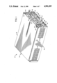
- FIG. 1 is a perspective view of the exterior of the housing for electronic components of the present invention.
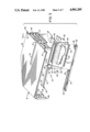
- FIG. 2 is a perspective view of the lower housing member.
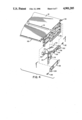
- FIG. 3 is an exploded perspective view of the upper housing member, also showing an internal frame and circuit boards.
- FIG. 4 is a fragmentary exploded perspective view showing one end of the upper housing member, and grounding elements associated therewith.
- FIG. 5 is a sectional view taken along line 5--5 of FIG. 3.
- FIG. 6 is a sectional view, taken along line 6--6 of FIG. 3.
- FIG. 7 is a fragmentary exploded perspective view, showing a fastening mechanism for securing a circuit board to the base of the lower housing member.
- FIG. 8 is a sectional view of the fastening mechanism of FIG. 7.
- FIG. 9 is a fragmentary sectional view taken along line 9--9 of FIG. 4, showing the ground planes in assembled relation to the ground connection.
- the housing 20 for electronic components. As may also be seen in FIGS. 2 and 3, the housing 20 includes an upper housing member 22 and a lower housing member 24.
- the lower housing member 24 includes a base 26 and two side walls 28 and 30.
- the side walls are provided with slots 32 to provide ventilation so that temperatures within the enclosure will not reach excessive levels.
- the side walls 28 and 30 are turned slightly inwardly to provide end elements 34 and 36.
- tabs 38 and 40 which are integral with the side walls 28 and 30, are turned inwardly at ninety degrees to provide a mounting for latches 42 and 44, which function to secure the upper housing member 22 and the lower housing member 24 together, as will subsequently be described in greater detail.
- a fastener (not shown) cooperates with a slot 55 in said projection 53 to achieve said retention.
- Three flexible spring elements 57 are also attached to the front edge of the base 26. These elements engages the end wall of the upper housing member 22 when the members 22 and 24 are assembled, in order to assure an electrical grounding contact between the two members.
- a processor circuit board 52 is secured to the base 26 by a plurality of downwardly extending fasteners 54 (FIGS. 7 and 8), which engage with slots56 located in circular raised areas 58 in the base 26.
- the slots 56 are wider at their open ends than at their closed ends in order to facilitate initial placement of the fasteners 54 therein.
- Each fastener 54 has a resilient upper portion 58 which is pushed through an aperture 60 in the board 52 and then springs outwardly to retain the fastener 54 in place.
- a central shaft 62 of the fastener 54 has a retainer 64 at the upper end thereof which engages the lower surface of the board 52 when the fastener 54 is secured to the base 26.
- a flange 66 and a cap 68 on the shaft 62 define therebetween a portion of the shaft 62 which engages the slot 56 inthe raised area 58 of the base 26.
- the processor board 52 is a circuit board on which are mounted integrated circuit elements and other components such as those identified by reference characters 70, 72, 74 and 76 in FIG. 3. These components, together with conducting paths connecting them, comprise a substantial part of the circuitry included in the personal computer or other apparatuswhich includes the enclosure 20. Also mounted on the board are a pair of receptacles 78 and 80 which receive the edge connectors of one or more additional circuit boards, which are positioned in perpendicular relationship to the board 52, as will be subsequently described in greaterdetail. At its right end, as viewed in FIGS.
- the processor board 52 has attached thereto, by screws or other suitable securing means (not shown), a face member 82 which is apertured to accommodate a number of plugs or receptacles for interfacing electronic components within the housing 20 with electrical circuitry outside the housing 20.
- plugs or receptacles can be employed for any suitable interconnection.
- a plug 84 is provided for communications
- a plug 86 is provided for the CRT
- a plug 88 is provided for a cash drawer
- a plug 90 is provided for a printer module
- a plug 92 is provided for a keyboard
- a plug 94 is provided for a power supply.
- the upper housing member 22 includes a flat cover portion 96, a depending integral front wall 98, and a rear frame 100, which is secured to the cover portion 96 by welding or other suitable means.
- the rear wall 98 is provided with slots 102 for ventilating purposes, and is also provided with slots 104 which engage with the projections 50 on the lower housing member 24 for securing the members 22 and 24 together.
- End walls 106 on the front wall 98 are bent ninety degrees from the wall 98 and overlie theend elements 34 and 36 of the walls 28 and 30 of the lower housing member 24 when the members 22 and 24 are in assembled relationship.
- the side edges of the flat cover portion 96 are turned downwardly to form flanges 108 which overlie upper edge elements 46 and 48 when the upper andlower housing members 22 and 24 are in assembled relationship.
- Two slots 110 are formed near the rear edge of the cover portion 96 and arepositioned to receive upper hook portions of latches 42 and 44.
- the latches42 and 44 are of a toggle type of construction, so that when the hook portions of these latches are engaged in the slots 110 and the latches 42 and 44 are moved downwardly by toggle action, the upper housing member 22 is latched securely to the lower housing member 24.
- a tab 111 which extends from the rear edge of the cover portion 96, includes an integral stiffened portion 113, and may be readily grasped at the same time that the tab 41 on the lower housing members 24 is grasped, in order to separate the upper and lower housing members.
- a large central slot 112 is also provided in the cover portion 96 and permits engagement by an external electrical connector with a vertically positioned circuit board which is located within the housing 20, as will subsequently be disclosed in greater detail.
- a vertical circuit board frame 114 Secured to the underside of the cover portion 96, to the rear wall 98, and to the frame 100 is a vertical circuit board frame 114 which includes an upper element 116 and a lower element 118.
- the upper element 116 may be secured to the lower surface of the cover portion 96 by welding, for example, and may be secured to the rear wall 98 and to the frame 100 by tabs 120 and 122, respectively, also by welding.
- the lower element 118 maybe secured to the rear wall 98 and to the frame 100 by tabs 124 and 126, respectively, also by welding.
- the frame 114 is provided to hold a bus circuit board 128 in a central vertical position within the housing 20 so that connectors 130, 132 on thebottom edge of said board will engage the slots 134, 136 of the receptacles78, 80 on the board 52 when the upper and lower housing members 22, 24 are in assembled relationship.
- Apertures 138 in the frame elements 116 and 118 are positioned to register with apertures 140 in the circuit board 128 whensaid board is properly positioned, and resilient connectors 142 may then beused to secure the board 128 in place on the frame 114.
- the bus board 128 serves a busing function in providing communication between a plurality of additional circuit boards, which are plugged into the board 128, and the processor board 52, into which the bus board 128 isplugged by the connectors 130, 132 and the receptacles 78, 80, as previously described.
- a plurality of receptacles such as the receptacles 144, 146, 148, 150 and 152 (see FIG. 5), are secured to the board 128 in ahorizontal orientation, so that additional circuit boards, such as the boards 154, 156, 158, 160 and 162, when plugged into the receptacles, are located in horizontal planes, parallel to the plane of the processor board52, within the housing 20.
- the boards 154, 156, 158, 160 and 162 are mounted on both sides of the bus board 128 and that the electrical components mountedon the boards, such as the components 164, 166, 168, 170 and 172, are mounted on opposite sides of adjacent boards. Both of these arrangements tend to maximize the number of boards which can be placed horizontally in the space between the processor board 52 and the cover portion 96.
- the boards 154, 156, 158, 160 and 162 can be of greater width, in their dimension extending away from the board 128, than they could be if they were mounted vertically and plugged directly into the processor board 52. Looking at the arrangement another way, it permitsthe upper and lower surfaces of the housing 20 to be closer together in a vertical dimension for a given width of boards 154, 156, 158, 160 and 162 than would be the case if the boards were mounted vertically. This enablesstandard sizes of boards used in personal computers, such as the IBM PCAT, for example, to be employed in a housing which is smaller in its vertical dimension than would normally be possible.
- the receptacles 144, 148 and 152 on one side of the bus board 128 are set back from the front vertical edge of the board 128 a lesser distance than the receptacles 146 and 150 on the other side of the bus board 128. This is to permit ground plates associated with the boards to overlap an engaging a central ground connection 174 which is mounted on the frame 100.
- the ground connection 174 comprises a pair of U-shaped elements 176 and 178 which are secured together.
- a ground plate 180 is electrically connected to the circuit board 154 and has an angled end portion 202 which is connected to the frame 100 by suitable means, such asscrews 182.
- Apertures in the ground plate 180 are surrounded by connectors 184 and 186 which may be coupled to the shielding of external circuitry.
- Connectors (not shown), electrically connected to the circuit board 154, extend through the apertures in the ground plate 180 for connection to external electrical conductors.
- the free end of the ground plate 180 electrically engages an internal surface of the U-shaped element 178.
- a ground plate 188 is connected to the board 156.
- An angledend portion 204 of the plate 188 is connected by screws 200 to the frame 100.
- the free end of the ground plate 188 electrically engages the outer surface of the U-shaped element 176. It will be seen that providing a structure in which the free ends of the ground plates 180 and 188, which are associated with the circuit boards 154 and 156, overlap enhances the compactness of the housing 20.
Abstract
Description
Claims (22)
Priority Applications (3)
| Application Number | Priority Date | Filing Date | Title |
|---|---|---|---|
| US07/239,818 US4901205A (en) | 1988-09-02 | 1988-09-02 | Housing for electronic components |
| JP1220519A JPH02113597A (en) | 1988-09-02 | 1989-08-29 | Electronic component housing |
| EP89308695A EP0357362A3 (en) | 1988-09-02 | 1989-08-29 | Housing for electronic components |
Applications Claiming Priority (1)
| Application Number | Priority Date | Filing Date | Title |
|---|---|---|---|
| US07/239,818 US4901205A (en) | 1988-09-02 | 1988-09-02 | Housing for electronic components |
Publications (1)
| Publication Number | Publication Date |
|---|---|
| US4901205A true US4901205A (en) | 1990-02-13 |
Family
ID=22903879
Family Applications (1)
| Application Number | Title | Priority Date | Filing Date |
|---|---|---|---|
| US07/239,818 Expired - Lifetime US4901205A (en) | 1988-09-02 | 1988-09-02 | Housing for electronic components |
Country Status (3)
| Country | Link |
|---|---|
| US (1) | US4901205A (en) |
| EP (1) | EP0357362A3 (en) |
| JP (1) | JPH02113597A (en) |
Cited By (38)
| Publication number | Priority date | Publication date | Assignee | Title |
|---|---|---|---|---|
| US5045977A (en) * | 1989-09-19 | 1991-09-03 | Bull S.A. | Shielding assembly for a terminal strip connected to an electrical device located inside a chassis |
| US5051868A (en) * | 1990-07-25 | 1991-09-24 | Sun Microsystems, Inc. | Computer construction |
| US5121296A (en) * | 1991-06-10 | 1992-06-09 | Kai Hsu | Computer housing assembly which can be assembled and disassembled without tools |
| US5130893A (en) * | 1990-01-17 | 1992-07-14 | Square D Company | Signal distribution system |
| US5163833A (en) * | 1989-04-14 | 1992-11-17 | Digital Communications Associates, Inc. | Dual personal computer architecture peripheral adapter board |
| US5191544A (en) * | 1990-06-15 | 1993-03-02 | International Business Machines Corp. | Personal computer enclosure with shielding |
| EP0534921A1 (en) * | 1991-09-27 | 1993-03-31 | Telefonaktiebolaget L M Ericsson | An RFI through-let for screening signals |
| US5214569A (en) * | 1991-09-06 | 1993-05-25 | Hsiang Lin C | Mother board structure with fitting holes |
| US5227582A (en) * | 1992-04-06 | 1993-07-13 | Digital Equipment Corporation | Video amplifier assembly mount |
| US5258889A (en) * | 1992-09-28 | 1993-11-02 | Ford Motor Company | Apparatus for compliantly retaining a circuit board in a housing |
| US5287460A (en) * | 1989-04-14 | 1994-02-15 | Digital Communications Associates, Inc. | Bus interface circuit for dual personal computer architecture peripheral adapter board |
| US5338214A (en) * | 1992-10-27 | 1994-08-16 | Steffes Karl M | Expansion card/riser card module for desktop computers |
| US5353202A (en) * | 1990-07-20 | 1994-10-04 | International Business Machines Corp. | Personal computer with shielding of input/output signals |
| US5357404A (en) * | 1991-11-18 | 1994-10-18 | The Whitaker Corporation | EMI shield, and assembly using same |
| US5383096A (en) * | 1993-05-03 | 1995-01-17 | Digital Equipment Corporation | I/O expansion box |
| WO1995019673A1 (en) * | 1994-01-14 | 1995-07-20 | Elonex Technologies, Inc. | Communications network system of client node array linked to resource server node array |
| US5442520A (en) * | 1994-07-01 | 1995-08-15 | Cincinnnati Milacron Inc. | Apparatus for printed circuit board connection |
| US5497292A (en) * | 1994-10-14 | 1996-03-05 | Dell Usa, L.P. | Configurable computer chassis port and method of manufacture therefor |
| US5496181A (en) * | 1993-05-14 | 1996-03-05 | International Business Machines Corporation | Serviceable data terminal structure |
| US5579210A (en) * | 1995-05-05 | 1996-11-26 | At&T Global Information Solutions Company | Apparatus and method for covering interface openings in a computer housing |
| US5686695A (en) * | 1996-03-15 | 1997-11-11 | Enlight Corporation | Resilient plate for a computer interface card |
| US6178093B1 (en) * | 1996-06-28 | 2001-01-23 | International Business Machines Corporation | Information handling system with circuit assembly having holes filled with filler material |
| US6186800B1 (en) | 1999-01-13 | 2001-02-13 | Micron Electronics, Inc. | Circuit board grounding and support structure |
| US6288329B1 (en) * | 1997-08-20 | 2001-09-11 | Dmt Gmbh, Feinwerktechnische Komplettlosungen | Folding component housing |
| US6308394B1 (en) | 1997-12-11 | 2001-10-30 | Micron Technology, Inc. | Method of mounting a motherboard to a chassis |
| US6345994B1 (en) | 1999-01-13 | 2002-02-12 | Micron Technology, Inc. | Circuit board support clip |
| US6362978B1 (en) | 1999-12-27 | 2002-03-26 | Micron Technology, Inc. | Method and apparatus for biasing a circuit board into engagement with a computer chassis |
| US6490725B2 (en) | 1994-01-14 | 2002-12-03 | Elonex I.P. Holdings, Ltd. | Transmitting notification of new video clips of interest from servers in wide area network |
| US6535394B1 (en) * | 1999-04-19 | 2003-03-18 | Hewlett-Packard Company | Printed circuit board attachment structure |
| US6771516B1 (en) | 1999-12-27 | 2004-08-03 | Micron Technology, Inc. | Method and apparatus for fastening circuit boards to computer chassis |
| US20070020962A1 (en) * | 2005-07-20 | 2007-01-25 | Alps Electric Co., Ltd. | Connecting element and circuit connecting device using the connecting element |
| US20070194021A1 (en) * | 2006-02-22 | 2007-08-23 | Chien-Fa Liang | Modular case assembly device |
| US20070201008A1 (en) * | 2005-11-23 | 2007-08-30 | Hsien-Feng Lin | Projection Device with an Electromagnetic Interference Shielding Slice |
| US20070236903A1 (en) * | 2006-04-07 | 2007-10-11 | Sean Phillip Hall | Small-frame computer with overlapping add-in cards |
| US20120327579A1 (en) * | 2011-06-22 | 2012-12-27 | Hon Hai Precision Industry Co., Ltd. | Computer chassis for mounting motherboard therein |
| US20130147327A1 (en) * | 2010-08-23 | 2013-06-13 | Rohde & Schwarz Gmbh & Co. Kg | Box-frame housing and a method of manufacture |
| CN114845506A (en) * | 2022-06-01 | 2022-08-02 | 广州粤道智能科技发展有限公司 | Network communication equipment cabinet convenient to maintain |
| USD980804S1 (en) * | 2020-12-23 | 2023-03-14 | Arista Networks, Inc. | Electrical housing |
Families Citing this family (5)
| Publication number | Priority date | Publication date | Assignee | Title |
|---|---|---|---|---|
| US4979075A (en) * | 1989-10-12 | 1990-12-18 | Compuadd, Corporation | Method and apparatus for controlling circuit expansion for consumer electronic systems |
| JPH09282049A (en) * | 1996-04-15 | 1997-10-31 | Pfu Ltd | Casing for information processor |
| FR2784213A1 (en) * | 1998-10-02 | 2000-04-07 | Alphalogic | Microcomputer-type cash register terminal, for use by several employees in restaurant or similar, has flat touch screen mounted on base part housing electronic components with defined cooling air paths |
| JP5723992B2 (en) * | 2012-08-29 | 2015-05-27 | Eizo株式会社 | AC inlet grounding method and AC inlet grounding structure |
| DE102014222951B4 (en) | 2014-11-11 | 2016-07-28 | Würth Elektronik eiSos Gmbh & Co. KG | Fastening element for attachment to a printed circuit board and fastening device and method for spaced connection of printed circuit boards with such a fastener |
Citations (10)
| Publication number | Priority date | Publication date | Assignee | Title |
|---|---|---|---|---|
| US3811154A (en) * | 1973-02-26 | 1974-05-21 | R Lindeman | Panel mounting fastener |
| US3836703A (en) * | 1973-10-19 | 1974-09-17 | Richco Plastic Co | Circuit board spacer-support |
| US4498717A (en) * | 1983-08-29 | 1985-02-12 | Gte Communication Systems Corp. | Printed wiring board interconnect arrangement |
| US4574332A (en) * | 1983-06-29 | 1986-03-04 | Calabro Anthony Denis | Cage apparatus for printed circuit boards and method for preventing sharp spikes in the signal applied to said printed circuit boards |
| US4585122A (en) * | 1985-01-28 | 1986-04-29 | Racal Data Communications, Inc. | Secure housing arrangement for electronic apparatus |
| US4652969A (en) * | 1985-07-05 | 1987-03-24 | Racal Data Communications Inc. | Secure universal housing arrangement for enclosing electronic circuits |
| US4672510A (en) * | 1984-10-19 | 1987-06-09 | Burr-Brown Corporation | Package for an expandable remote interface unit |
| US4717216A (en) * | 1985-08-13 | 1988-01-05 | General Datacomm, Inc. | Multi circuit board card enclosure |
| US4744006A (en) * | 1986-07-10 | 1988-05-10 | Duffield Robert H | Apparatus for expanding the input/output capabilities of a personal computer |
| US4745524A (en) * | 1987-04-24 | 1988-05-17 | Western Digital Corporation | Mounting of printed circuit boards in computers |
Family Cites Families (4)
| Publication number | Priority date | Publication date | Assignee | Title |
|---|---|---|---|---|
| JPS5890224A (en) * | 1981-11-24 | 1983-05-28 | Nec Corp | Electronic device |
| DE3332658A1 (en) * | 1983-09-09 | 1985-03-28 | Siemens AG, 1000 Berlin und 8000 München | Latching spring |
| EP0170853A1 (en) * | 1984-07-06 | 1986-02-12 | Siemens Aktiengesellschaft | Electrical component |
| JPH06862Y2 (en) * | 1987-07-03 | 1994-01-05 | 北川工業株式会社 | Spacer |
-
1988
- 1988-09-02 US US07/239,818 patent/US4901205A/en not_active Expired - Lifetime
-
1989
- 1989-08-29 JP JP1220519A patent/JPH02113597A/en active Pending
- 1989-08-29 EP EP89308695A patent/EP0357362A3/en not_active Withdrawn
Patent Citations (10)
| Publication number | Priority date | Publication date | Assignee | Title |
|---|---|---|---|---|
| US3811154A (en) * | 1973-02-26 | 1974-05-21 | R Lindeman | Panel mounting fastener |
| US3836703A (en) * | 1973-10-19 | 1974-09-17 | Richco Plastic Co | Circuit board spacer-support |
| US4574332A (en) * | 1983-06-29 | 1986-03-04 | Calabro Anthony Denis | Cage apparatus for printed circuit boards and method for preventing sharp spikes in the signal applied to said printed circuit boards |
| US4498717A (en) * | 1983-08-29 | 1985-02-12 | Gte Communication Systems Corp. | Printed wiring board interconnect arrangement |
| US4672510A (en) * | 1984-10-19 | 1987-06-09 | Burr-Brown Corporation | Package for an expandable remote interface unit |
| US4585122A (en) * | 1985-01-28 | 1986-04-29 | Racal Data Communications, Inc. | Secure housing arrangement for electronic apparatus |
| US4652969A (en) * | 1985-07-05 | 1987-03-24 | Racal Data Communications Inc. | Secure universal housing arrangement for enclosing electronic circuits |
| US4717216A (en) * | 1985-08-13 | 1988-01-05 | General Datacomm, Inc. | Multi circuit board card enclosure |
| US4744006A (en) * | 1986-07-10 | 1988-05-10 | Duffield Robert H | Apparatus for expanding the input/output capabilities of a personal computer |
| US4745524A (en) * | 1987-04-24 | 1988-05-17 | Western Digital Corporation | Mounting of printed circuit boards in computers |
Cited By (48)
| Publication number | Priority date | Publication date | Assignee | Title |
|---|---|---|---|---|
| US5287460A (en) * | 1989-04-14 | 1994-02-15 | Digital Communications Associates, Inc. | Bus interface circuit for dual personal computer architecture peripheral adapter board |
| US5163833A (en) * | 1989-04-14 | 1992-11-17 | Digital Communications Associates, Inc. | Dual personal computer architecture peripheral adapter board |
| US5045977A (en) * | 1989-09-19 | 1991-09-03 | Bull S.A. | Shielding assembly for a terminal strip connected to an electrical device located inside a chassis |
| US5130893A (en) * | 1990-01-17 | 1992-07-14 | Square D Company | Signal distribution system |
| US5191544A (en) * | 1990-06-15 | 1993-03-02 | International Business Machines Corp. | Personal computer enclosure with shielding |
| US5353202A (en) * | 1990-07-20 | 1994-10-04 | International Business Machines Corp. | Personal computer with shielding of input/output signals |
| US5051868A (en) * | 1990-07-25 | 1991-09-24 | Sun Microsystems, Inc. | Computer construction |
| US5121296A (en) * | 1991-06-10 | 1992-06-09 | Kai Hsu | Computer housing assembly which can be assembled and disassembled without tools |
| US5214569A (en) * | 1991-09-06 | 1993-05-25 | Hsiang Lin C | Mother board structure with fitting holes |
| EP0534921A1 (en) * | 1991-09-27 | 1993-03-31 | Telefonaktiebolaget L M Ericsson | An RFI through-let for screening signals |
| US5404276A (en) * | 1991-09-27 | 1995-04-04 | Telefonaktiebolaget L M Ericsson | Screened RFI through-let |
| US5357404A (en) * | 1991-11-18 | 1994-10-18 | The Whitaker Corporation | EMI shield, and assembly using same |
| US5227582A (en) * | 1992-04-06 | 1993-07-13 | Digital Equipment Corporation | Video amplifier assembly mount |
| US5258889A (en) * | 1992-09-28 | 1993-11-02 | Ford Motor Company | Apparatus for compliantly retaining a circuit board in a housing |
| US5338214A (en) * | 1992-10-27 | 1994-08-16 | Steffes Karl M | Expansion card/riser card module for desktop computers |
| US5383096A (en) * | 1993-05-03 | 1995-01-17 | Digital Equipment Corporation | I/O expansion box |
| US5496181A (en) * | 1993-05-14 | 1996-03-05 | International Business Machines Corporation | Serviceable data terminal structure |
| US6490725B2 (en) | 1994-01-14 | 2002-12-03 | Elonex I.P. Holdings, Ltd. | Transmitting notification of new video clips of interest from servers in wide area network |
| US5515510A (en) * | 1994-01-14 | 1996-05-07 | Consilium Overseas Limited | Communications internetwork system connecting a client node array to a resource array |
| WO1995019673A1 (en) * | 1994-01-14 | 1995-07-20 | Elonex Technologies, Inc. | Communications network system of client node array linked to resource server node array |
| US5442520A (en) * | 1994-07-01 | 1995-08-15 | Cincinnnati Milacron Inc. | Apparatus for printed circuit board connection |
| US5497292A (en) * | 1994-10-14 | 1996-03-05 | Dell Usa, L.P. | Configurable computer chassis port and method of manufacture therefor |
| US5579210A (en) * | 1995-05-05 | 1996-11-26 | At&T Global Information Solutions Company | Apparatus and method for covering interface openings in a computer housing |
| US5686695A (en) * | 1996-03-15 | 1997-11-11 | Enlight Corporation | Resilient plate for a computer interface card |
| US6178093B1 (en) * | 1996-06-28 | 2001-01-23 | International Business Machines Corporation | Information handling system with circuit assembly having holes filled with filler material |
| US6288329B1 (en) * | 1997-08-20 | 2001-09-11 | Dmt Gmbh, Feinwerktechnische Komplettlosungen | Folding component housing |
| US6470555B2 (en) | 1997-12-11 | 2002-10-29 | Micron Technology, Inc. | Method of mounting a motherboard to chassis |
| US6308394B1 (en) | 1997-12-11 | 2001-10-30 | Micron Technology, Inc. | Method of mounting a motherboard to a chassis |
| US6470556B2 (en) | 1997-12-11 | 2002-10-29 | Micron Technology, Inc. | Method removably mounting a planar component to a chassis |
| US6186800B1 (en) | 1999-01-13 | 2001-02-13 | Micron Electronics, Inc. | Circuit board grounding and support structure |
| US6345994B1 (en) | 1999-01-13 | 2002-02-12 | Micron Technology, Inc. | Circuit board support clip |
| US6535394B1 (en) * | 1999-04-19 | 2003-03-18 | Hewlett-Packard Company | Printed circuit board attachment structure |
| US6362978B1 (en) | 1999-12-27 | 2002-03-26 | Micron Technology, Inc. | Method and apparatus for biasing a circuit board into engagement with a computer chassis |
| US6771516B1 (en) | 1999-12-27 | 2004-08-03 | Micron Technology, Inc. | Method and apparatus for fastening circuit boards to computer chassis |
| US7331798B2 (en) * | 2005-07-20 | 2008-02-19 | Alps Electric Co., Ltd. | Connecting element and circuit connecting device using the connecting element |
| US20070020962A1 (en) * | 2005-07-20 | 2007-01-25 | Alps Electric Co., Ltd. | Connecting element and circuit connecting device using the connecting element |
| US20070201008A1 (en) * | 2005-11-23 | 2007-08-30 | Hsien-Feng Lin | Projection Device with an Electromagnetic Interference Shielding Slice |
| US20070194021A1 (en) * | 2006-02-22 | 2007-08-23 | Chien-Fa Liang | Modular case assembly device |
| US7735669B2 (en) * | 2006-02-22 | 2010-06-15 | Super Micro Computer Inc. | Modular case assembly device |
| US20070236903A1 (en) * | 2006-04-07 | 2007-10-11 | Sean Phillip Hall | Small-frame computer with overlapping add-in cards |
| US7359216B2 (en) * | 2006-04-07 | 2008-04-15 | Sean Phillip Hall | Small-frame computer with overlapping add-in cards |
| US10321595B2 (en) | 2010-08-23 | 2019-06-11 | Rohde & Schwarz Gmbh & Co. Kg | Box-frame housing and a method of manufacture |
| US20130147327A1 (en) * | 2010-08-23 | 2013-06-13 | Rohde & Schwarz Gmbh & Co. Kg | Box-frame housing and a method of manufacture |
| US9167713B2 (en) * | 2010-08-23 | 2015-10-20 | Rohde & Schwarz Gmbh & Co. Kg | Box-frame housing and a method of manufacture |
| US20120327579A1 (en) * | 2011-06-22 | 2012-12-27 | Hon Hai Precision Industry Co., Ltd. | Computer chassis for mounting motherboard therein |
| USD980804S1 (en) * | 2020-12-23 | 2023-03-14 | Arista Networks, Inc. | Electrical housing |
| CN114845506A (en) * | 2022-06-01 | 2022-08-02 | 广州粤道智能科技发展有限公司 | Network communication equipment cabinet convenient to maintain |
| CN114845506B (en) * | 2022-06-01 | 2024-02-23 | 广州粤道智能科技发展有限公司 | Network communication equipment cabinet convenient for maintenance |
Also Published As
| Publication number | Publication date |
|---|---|
| EP0357362A3 (en) | 1990-04-25 |
| EP0357362A2 (en) | 1990-03-07 |
| JPH02113597A (en) | 1990-04-25 |
Similar Documents
| Publication | Publication Date | Title |
|---|---|---|
| US4901205A (en) | Housing for electronic components | |
| JP2514241B2 (en) | Circuit card housing device | |
| US4821145A (en) | Pluggable assembly for printed circuit cards | |
| US6238244B1 (en) | Shielded electrical connector with superposed terminals | |
| US7742291B2 (en) | Computer enclosure adapted for mounting different types of transfer cards | |
| US5734551A (en) | Method to install SIMMs without causing discomfort to the user | |
| US5940275A (en) | PCMCIA card frame connector and cover assembly | |
| US5333100A (en) | Data card perimeter shield | |
| US6297955B1 (en) | Host assembly for an integrated computer module | |
| US6411522B1 (en) | Integrated computer module with EMI shielding plate | |
| US5339222A (en) | Shielded printed circuit card holder | |
| TW256954B (en) | Improved grounding shroud for electrical connectors | |
| US6049973A (en) | Method of assembling an integrated computer module | |
| JP2844530B2 (en) | Shield for IC card | |
| US5695362A (en) | Hybrid grounded and stacked connector assembly with audio jacks | |
| US7258574B2 (en) | Snap-fit electromagnetic shield | |
| JPH08236215A (en) | Universal ground clip for card acceptance connector | |
| TW200525833A (en) | Electrical card connector | |
| US20120168223A1 (en) | Housing system for receptacles | |
| EP0520173A2 (en) | Computer housing | |
| KR970008504B1 (en) | Connector | |
| US5299942A (en) | Input-output electrical connector | |
| US5793620A (en) | Computer extension board connected to an expansion board | |
| US20040130864A1 (en) | Electronic apparatus having lid to cover memory receptacle | |
| US5465934A (en) | Bracket for a CPU daughter card |
Legal Events
| Date | Code | Title | Description |
|---|---|---|---|
| AS | Assignment |
Owner name: NCR CORPORATION, DAYTON, OHIO, A CORP. OF MARYLAND Free format text: ASSIGNMENT OF ASSIGNORS INTEREST.;ASSIGNORS:LANDIS, DONALD E.;ATKINSON, JAY D.;LYONS, DALE R.;AND OTHERS;REEL/FRAME:004974/0312;SIGNING DATES FROM 19880823 TO 19880826 Owner name: NCR CORPORATION, A CORP. OF MARYLAND, OHIO Free format text: ASSIGNMENT OF ASSIGNORS INTEREST;ASSIGNORS:LANDIS, DONALD E.;ATKINSON, JAY D.;LYONS, DALE R.;AND OTHERS;SIGNING DATES FROM 19880823 TO 19880826;REEL/FRAME:004974/0312 |
|
| STCF | Information on status: patent grant |
Free format text: PATENTED CASE |
|
| CC | Certificate of correction | ||
| FPAY | Fee payment |
Year of fee payment: 4 |
|
| FPAY | Fee payment |
Year of fee payment: 8 |
|
| FPAY | Fee payment |
Year of fee payment: 12 |