US4901267A - Floating point circuit with configurable number of multiplier cycles and variable divide cycle ratio - Google Patents
Floating point circuit with configurable number of multiplier cycles and variable divide cycle ratio Download PDFInfo
- Publication number
- US4901267A US4901267A US07/167,802 US16780288A US4901267A US 4901267 A US4901267 A US 4901267A US 16780288 A US16780288 A US 16780288A US 4901267 A US4901267 A US 4901267A
- Authority
- US
- United States
- Prior art keywords
- divide
- clock
- multiplier
- input
- coupled
- Prior art date
- Legal status (The legal status is an assumption and is not a legal conclusion. Google has not performed a legal analysis and makes no representation as to the accuracy of the status listed.)
- Expired - Lifetime
Links
Images

Classifications
-
- G—PHYSICS
- G06—COMPUTING; CALCULATING OR COUNTING
- G06F—ELECTRIC DIGITAL DATA PROCESSING
- G06F9/00—Arrangements for program control, e.g. control units
- G06F9/06—Arrangements for program control, e.g. control units using stored programs, i.e. using an internal store of processing equipment to receive or retain programs
- G06F9/30—Arrangements for executing machine instructions, e.g. instruction decode
- G06F9/38—Concurrent instruction execution, e.g. pipeline, look ahead
- G06F9/3885—Concurrent instruction execution, e.g. pipeline, look ahead using a plurality of independent parallel functional units
-
- G—PHYSICS
- G06—COMPUTING; CALCULATING OR COUNTING
- G06F—ELECTRIC DIGITAL DATA PROCESSING
- G06F1/00—Details not covered by groups G06F3/00 - G06F13/00 and G06F21/00
- G06F1/04—Generating or distributing clock signals or signals derived directly therefrom
- G06F1/12—Synchronisation of different clock signals provided by a plurality of clock generators
-
- G—PHYSICS
- G06—COMPUTING; CALCULATING OR COUNTING
- G06F—ELECTRIC DIGITAL DATA PROCESSING
- G06F7/00—Methods or arrangements for processing data by operating upon the order or content of the data handled
- G06F7/38—Methods or arrangements for performing computations using exclusively denominational number representation, e.g. using binary, ternary, decimal representation
- G06F7/48—Methods or arrangements for performing computations using exclusively denominational number representation, e.g. using binary, ternary, decimal representation using non-contact-making devices, e.g. tube, solid state device; using unspecified devices
- G06F7/483—Computations with numbers represented by a non-linear combination of denominational numbers, e.g. rational numbers, logarithmic number system or floating-point numbers
-
- G—PHYSICS
- G06—COMPUTING; CALCULATING OR COUNTING
- G06F—ELECTRIC DIGITAL DATA PROCESSING
- G06F7/00—Methods or arrangements for processing data by operating upon the order or content of the data handled
- G06F7/38—Methods or arrangements for performing computations using exclusively denominational number representation, e.g. using binary, ternary, decimal representation
- G06F7/48—Methods or arrangements for performing computations using exclusively denominational number representation, e.g. using binary, ternary, decimal representation using non-contact-making devices, e.g. tube, solid state device; using unspecified devices
- G06F7/57—Arithmetic logic units [ALU], i.e. arrangements or devices for performing two or more of the operations covered by groups G06F7/483 – G06F7/556 or for performing logical operations
-
- G—PHYSICS
- G06—COMPUTING; CALCULATING OR COUNTING
- G06F—ELECTRIC DIGITAL DATA PROCESSING
- G06F9/00—Arrangements for program control, e.g. control units
- G06F9/06—Arrangements for program control, e.g. control units using stored programs, i.e. using an internal store of processing equipment to receive or retain programs
- G06F9/30—Arrangements for executing machine instructions, e.g. instruction decode
- G06F9/30003—Arrangements for executing specific machine instructions
- G06F9/30007—Arrangements for executing specific machine instructions to perform operations on data operands
- G06F9/3001—Arithmetic instructions
- G06F9/30014—Arithmetic instructions with variable precision
-
- G—PHYSICS
- G06—COMPUTING; CALCULATING OR COUNTING
- G06F—ELECTRIC DIGITAL DATA PROCESSING
- G06F2207/00—Indexing scheme relating to methods or arrangements for processing data by operating upon the order or content of the data handled
- G06F2207/38—Indexing scheme relating to groups G06F7/38 - G06F7/575
- G06F2207/3804—Details
- G06F2207/3808—Details concerning the type of numbers or the way they are handled
- G06F2207/3812—Devices capable of handling different types of numbers
- G06F2207/382—Reconfigurable for different fixed word lengths
-
- G—PHYSICS
- G06—COMPUTING; CALCULATING OR COUNTING
- G06F—ELECTRIC DIGITAL DATA PROCESSING
- G06F2207/00—Indexing scheme relating to methods or arrangements for processing data by operating upon the order or content of the data handled
- G06F2207/38—Indexing scheme relating to groups G06F7/38 - G06F7/575
- G06F2207/3804—Details
- G06F2207/386—Special constructional features
- G06F2207/3884—Pipelining
Definitions
- the present invention relates to timing circuits for multiplier and divide/square root units in floating point systems.
- a typical floating point system will have both a multiplier (MUL) and an arithmetic logic unit (ALU).
- Multiplication requires the summation of many partial products, which makes the time to complete a MUL operation longer than the time for an ALU operation.
- Some systems require the clock cycle time to be as fast as possible which results in multiplication taking more cycles than addition.
- Other systems require a simple programming model with the same number of cycles for both multiplication and ALU operations. This results in more clock cycles being allocated for an ALU operation than are necessary.
- a divide/square root unit shares the same input stage as the multiplier unit and provides its result to succeeding stages of the multiplier unit.
- Such a divide/square root unit typically requires a fixed number of cycles for an operation, so that control circuitry clocks in the operands and then clocks out the result after counting the required number of cycles.
- a multiplier may have three stages in one system, an input stage, an output stage and an intermediate stage with a fixed-point half-array multiplier.
- a register at the beginning of the output stage has its output fed back to a multiplexer in the intermediate stage to allow a second pass through the half-array for double-precision floating-point and integer multiplications.
- Single-precision and mixed-precision multiplications require only one pass through the array.
- the present invention optimizes the number and ratio of cycles required among the divide/square root unit, multiplier unit and ALU.
- An intermediate latch with its own clock is provided at the output of the multiplier half-array in the intermediate stage to feed back data for a second pass for double-precision numbers.
- the multiplier can then be adjusted for either two-cycle latency mode (for optimizing double-precision multiplies) or three-cycle latency mode (for optimizing single-precision multiplies).
- a separate divide clock is used for the divide/square root unit, and is synchronized with the multiplier cycle clock on input and output. This allows the divide time to be optimized so that it requires fewer clock cycles when a longer multiplier clock cycle time is used.
- the present invention thus allows a user to optimize the circuit for the application expected.
- the three-cycle latency mode allows a shorter cycle time for single-precision floating-point operations.
- the invention allows a system designer to get the optimum performance out of the divide square root unit for any particular clock rate for the device. Provided that the device major clock cycle time is long enough, the divide iteration rate is completely independent of the multiplier or ALU configuration. Divide iterations can be formed at a rate that is any positive integer multiple of the ALU/MUL instruction rate.
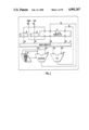
- FIG. 1 is a block diagram of a floating-point data path which uses the present invention
- FIG. 2 is a more detailed block diagram of the embodiment of FIG. 1 showing the present invention
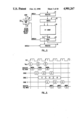
- FIG. 3 is a block diagram of the multiplier array feedback
- FIG. 4 is a block diagram of the synchronizing circuits for the divide clock
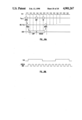
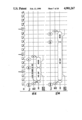
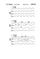
- FIG. 5 is a timing diagram of the two-cycle latency mode for the multiplier
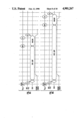
- FIG. 6 is a timing diagram of the three-cycle latency mode for the multiplier
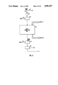
- FIG. 7 is a block diagram showing why two integer or double-precision floating point multiply instructions cannot follow each other in three-cycle latency modes
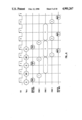
- FIGS. 8A-D are timing diagrams of the divide/square root unit
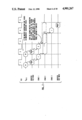
- FIGS. 9A-9C are timing diagrams of the clocks of FIG. 3.
- FIGS. 10A and 10B are timing diagrams of the divide/square root unit where the divide clock frequency is 8 ⁇ main clock frequency.
- FIG. 1 is a block diagram of a 64-bit floating-point data path which utilizes the present invention.
- a register file 12 and registers 14 and 16 provide input data to busing and multiplexing
- the divide/square root unit shares input and output circuitry with the multiplier.
- operands are clocked into divide/square root unit 24 and a counter is activated to clock out the result a fixed number of cycles later.
- the present invention uses a separate divide clock as shown in the more detailed block diagram of FIG. 2.
- multiplier 22 is pipelined with three stages, afirst stage 26, a second stage 28 and a third stage 30. There are also two pipeline registers 32 and 34. Every multiply operation passes through these stages and registers in succession.
- Stage 1 contains front-end circuits to detect source exceptions, e.g. denormalized numbers and invalid operations, and contains an adder to add exponents of floating-point numbers. If a source exception or an invalid operation is detected in stage one, floating-point exception output pin S6, FPEX-. will be asserted, to indicate the exception to the rest of the system.
- source exceptions e.g. denormalized numbers and invalid operations
- adder to add exponents of floating-point numbers. If a source exception or an invalid operation is detected in stage one, floating-point exception output pin S6, FPEX-. will be asserted, to indicate the exception to the rest of the system.
- Stage 2 contains a fixed-point half-array (54 ⁇ 27) multiplier to multiply integers or fractions of floating-point numbers. Single-precisionand mixed-precision floating-point multiplications take one pass through the array, while double-precision floating-point and integer multiplications take two passes. Stage 2 operation takes one or two entirecycles following the completion of stage 1 operation.
- Stage 3 contains IEEE rounding circuits and result exception circuits. The stage 3 operations always take place in the first half of a cycle following the completion of a stage 2 operation.
- the multiplier has two input ports and one output.
- the selection of input port operands is controlled by single-bit MAIN (multiplier A input) and MBIN (multiplier B input) multiplexer controls, which are two of the inputs to the chip.
- the sources of multiplier operands are X register 16, Y register 14 and the A and B ports of register file 12.
- the output of a third stage of the multiplier is placed on the D bus. This output is always routed to the D port of register file 12. This output can also be forwarded to the E port through bypass multiplexer 38 on a store operation. In certain operations, the output can be routed to one or both of temporary latches 40, 42 (T0, T1). These are used in a multiply-add operation. In register-to-register operations, the output can be forwardeddirectly to an input of the multiplier or the ALU through bypass multiplexer 38, bypassing register file 12.
- the multiplier can be adjusted to two latency modes.
- the latency is the number of clock cycles required to complete a multiply operation.
- the latency mode is controlled by a multiply latency mode bit in status register 44.
- the purpose of providing the two modes is to allow the user to optimize either single-precision or double-precision multiplications. It is possible to switch between the two multiplier latency modes by changing the value of the mode bit.
- stage 2 operation takes one cycle, with eachpass through the array occurring in approximately one half of a cycle or less.
- each pass is given an entire cycle and thus the stage 2 operation takes two entire cycles.
- the cycle itself can be shorter.
- FIG. 3 shows the circuitry which enables a change in the latency mode of the multiplier.
- Pipeline registers 32 and 34 at the input and output of the multiplier array are shown.
- the half-array itself is indicated as block 60.
- the input to the half-array is provided by multiplexer 62 and a latch 64 is provided between the output of array 60 and pipeline register 34.
- a clock generator circuit 66 provides clock signals to pipeline registers 32 and 34 and latch 64.
- Two data paths are provided from the output of array 60, a first data path 68 to latch 64 and a second data path 70 directly to pipeline register 34.
- the latency mode control bit on line 73 controls the clock signals. In the three-cycle latency mode, the clock signal to latch 64 is provided on each major clock signal.
- latch 64 In the two-cycle latency mode, latch 64 is clocked each half cycle so that two passes through the array are completed in one cycle.
- a timing diagram showing the relative timing of clocks CM1CLK+, CM2CLK+ and CM3CLK+ are shown in FIG. 9.
- FIG. 5 is a timing diagram of the two-cycle latency mode and FIG. 6 is a timing diagram of the three-cycle latency mode.
- FIG. 7 two integer or double-precision floating point multiply instructions may not follow each other in three-cycle latency mode because this would result in an overlap in stage 2.
- FIGS. 9A, 9B and 9C show the clock timing for the two-cycle mode, the three-cycle mode (double-precision following double-precision) and three-cycle mode (double-precision followed by single-precision).
- the clocks are identical for the two-cycle mode.
- TheCM2CLK signal is provided to a latch which is level triggered, not edged triggered like the registers. Accordingly, changes to the contents of the latch will be locked out after half of a clock cycle, thus allowing two passes through the array in a single cycle of the clock.
- an instruction starts (stage 1) at a time 61 and register 32 receives data on the rising edge of CM1CLK at a time 63. Whilethe CM2CLK signal is high at a time 65, the first pass is made through the array, and then CM2CLK goes low, preventing further changes to the data inthe latch, for the second pass through the half array. There is no rising edge of CM1CLK during this period, with the next rising edge occurring at a time 67 when the half array will again be available for data. For half of the time, the output of register 34 will be garbage, but this does not matter since it is not sent to the register file.
- FIG. 9C shows a double-precision multiply followed by a single-precision multiply in which the CM1CLK signal and the CM2CLK signal change from the mode of FIG. 9B during a period 69 to the mode of FIG. 9A during a period 71.
- Clock generation circuit 66 of FIG. 3 produces the waveforms of FIGS. 9A-9C, and can be implemented in any of a number of ways.
- the inputs are the latency mode bit 73 the CLK signal and a 64 bit integer multiply select signal 75 which tells the circuit whether there is a double-precision multiply or a single-precision multiply.
- Divide/square root unit 24 is provided with a separatedivide clock (DIVCLK+) 46.
- the rest of the circuitry receives a clock signal 48 (CLK+).
- CLK+ clock signal
- clock signal 48 is provided to an AND-gate 50 along with a divide start signal 52.
- the result is provided to a register 54 which is clocked by divide clock signal 46.
- the circuit assumes that the DIVIDE START signal becomes settled while the clock is high (during the first half of a major clock cycle).
- the output of register 54 provides a control signal to divide/square root unit 24 to start a DIV/SQRT operation upon the input of new data.
- the output of data is controlled by a divide stop signal to a latch 56 which is clocked by divide clock 46.
- the output of latch 56 is provided to a register 58 which is clocked by clock signal 48.
- the actual implementation of this circuitry contains other logic elements which are unrelated to the present invention and are accordingly not shown. However, the diagram of FIG. 4 shows the logical synchronization function.
- the same multiplexers 72, 74 that select multiplier operands also select the operands for the divide/square root (DSR) unit.
- the DSR also shares the multiplier's source exceptions circuits.
- the DSR's separate clock input, DIVCLK may operate at either the same (1X), or double (2X), or any integer times the frequency, of the main clock CLK.
- Divide operations are performed at the rate of two bits of the result fraction per DIVCLK cycle.
- Square root operations (SQRT) operate at the rate of one bit of the result fraction per DIVCLK cycle.
- FIGS. 8A-8D The timing for 32 and 64 bit divides and 32 and 64 bit square root operations are shown in FIGS. 8A-8D, respectively.
- a DSR operation (divide or SQRT) is clocked in on the risingedge of cycle 1.
- operand(s) are read from the register file, and in the second half of the cycle they are latched inthe DSR unit.
- the actual DSR loop starts on the rising edge of cycle 2. After the loop is completed in the DSR unit, its result is loaded into themultiplier stage 1, provided the multiplier is unoccupied.
- a NOP no operation
- the unload operation starts in the first half of cycle N
- the result is written in the register filed in the second halfof cycle N+2, so the entire unload operation takes three cycles. Once unload starts, it essentially "looks" like any other two-cycle latency multiplier operation. If the multiplier is occupied by another operation when the loop is complete and unload could be initiated, the DSR unit waits until the multiplier becomes available. The DSR result will be unloaded into the multiplier in the first "empty" timing slot in the multiplier after the Divide/Square Root Unit has finished its operation. The result of the DSR operation is stored in a register file location whose address is given by the instruction which started the operation.
- multiplier operation may be initiated on any cycle after the DSR instruction has been clocked in, other than the one containing NOP.
- the cycle containing the NOP may be used for anALU-only operation.
- DSRINP DSR operation In Progress
- SR 6 a special bit, called DSRINP (DSR operation In Progress) in the status register, SR 6 , is set in cycle 3; it is automatically cleared in the cycle preceding the one in which the DSR result is written into the register file.
- DIV32 FIG. 8A
- the latency count is from the DSR instruction to the first instruction thatcould use the result of the DSR operation as an operand.
- the result is written into the register file in the second half of cycle 11.
- an instruction that uses this result may be clocked in on the rising edge of cycle 11, using register file bypass.
- This instruction is denoted in FIG. 8A as C11; it could be any instruction, including another DSR operation. Therefore, in this case the latency is from rising edge of cycle 1 to that of cycle 11, which is 10 cycles. This reasoning applies equally to the other cases.
- the second operation may be clocked in on the code port only after the first operation propagated to stage 3 of the multiplier and generated any potential result exceptions. For example, if two single-precision divides must be executed consecutively, and the first one was initiated on cycle 1, then the second one may be initiated on cycle 11. Refer to FIG. 8A.
- N 1,2,3 . . . and the
- the divide clock can be any integral multiple of the system clock so long as the minimum divide clock time is maintained. Accordingly, where a longer system clock cycle is required, a smaller number of system clock cycles will be required to perform a divide operation.
- FIG. 10A An example of the Divide/Square Root timing when the Divide Clock frequencyis 8 times the main clock frequency (FIG. 10B) is shown in FIG. 10A.
- the loop For 64bit divide and 32 bit square root operations, the loop is 4 cycles and for 64 bit square root operations the loop is 7 cycles. Otherwise the timing is as set forth in FIG. 10A.
- the latency where the divide clock is 8 timesthe main clock frequency is:
Abstract
Description
______________________________________
Single-precision divide
                 10 cycles of CLK
Double-precision divide
                 17 cycles of CLK
Single-precision SQRT
                 16 cycles of CLK
Double-precision SQRT
                 30 cycles of CLK
______________________________________
Claims (7)
Priority Applications (2)
| Application Number | Priority Date | Filing Date | Title |
|---|---|---|---|
| US07/167,802 US4901267A (en) | 1988-03-14 | 1988-03-14 | Floating point circuit with configurable number of multiplier cycles and variable divide cycle ratio |
| JP1063394A JPH0214318A (en) | 1988-03-14 | 1989-03-14 | Floating point circuit having buildable number of multiplier cycles and variable division cycle ratio |
Applications Claiming Priority (1)
| Application Number | Priority Date | Filing Date | Title |
|---|---|---|---|
| US07/167,802 US4901267A (en) | 1988-03-14 | 1988-03-14 | Floating point circuit with configurable number of multiplier cycles and variable divide cycle ratio |
Publications (1)
| Publication Number | Publication Date |
|---|---|
| US4901267A true US4901267A (en) | 1990-02-13 |
Family
ID=22608893
Family Applications (1)
| Application Number | Title | Priority Date | Filing Date |
|---|---|---|---|
| US07/167,802 Expired - Lifetime US4901267A (en) | 1988-03-14 | 1988-03-14 | Floating point circuit with configurable number of multiplier cycles and variable divide cycle ratio |
Country Status (2)
| Country | Link |
|---|---|
| US (1) | US4901267A (en) |
| JP (1) | JPH0214318A (en) |
Cited By (30)
| Publication number | Priority date | Publication date | Assignee | Title |
|---|---|---|---|---|
| US5021985A (en) * | 1990-01-19 | 1991-06-04 | Weitek Corporation | Variable latency method and apparatus for floating-point coprocessor |
| US5038312A (en) * | 1988-11-14 | 1991-08-06 | Nec Corporation | Data processing system capable of performing vector/matrix processing and arithmetic processing unit incorporated therein |
| US5053987A (en) * | 1989-11-02 | 1991-10-01 | Zoran Corporation | Arithmetic unit in a vector signal processor using pipelined computational blocks |
| EP0450804A2 (en) * | 1990-04-02 | 1991-10-09 | Advanced Micro Devices, Inc. | Pipelined floating point processing unit |
| US5060182A (en) * | 1989-09-05 | 1991-10-22 | Cyrix Corporation | Method and apparatus for performing the square root function using a rectangular aspect ratio multiplier |
| US5111421A (en) * | 1990-02-26 | 1992-05-05 | General Electric Company | System for performing addition and subtraction of signed magnitude floating point binary numbers |
| US5123108A (en) * | 1989-09-11 | 1992-06-16 | Wang Laboratories, Inc. | Improved cpu pipeline having register file bypass and working register bypass on update/access address compare |
| US5128888A (en) * | 1990-04-02 | 1992-07-07 | Advanced Micro Devices, Inc. | Arithmetic unit having multiple accumulators |
| US5153848A (en) * | 1988-06-17 | 1992-10-06 | Bipolar Integrated Technology, Inc. | Floating point processor with internal free-running clock |
| US5159566A (en) * | 1989-09-05 | 1992-10-27 | Cyrix Corporation | Method and apparatus for performing the square root function using a rectangular aspect ratio multiplier |
| US5179531A (en) * | 1990-04-27 | 1993-01-12 | Pioneer Electronic Corporation | Accelerated digital signal processor |
| US5181186A (en) * | 1988-04-13 | 1993-01-19 | Al Ofi Moatad S | TPC computers |
| US5204962A (en) * | 1989-11-30 | 1993-04-20 | Mitsubishi Denki Kabushiki Kaisha | Processor with preceding operation circuit connected to output of data register |
| US5206823A (en) * | 1990-12-13 | 1993-04-27 | Micron Technology, Inc. | Apparatus to perform Newton iterations for reciprocal and reciprocal square root |
| US5220524A (en) * | 1990-12-13 | 1993-06-15 | Micron Technology, Inc. | Machine method to perform newton iterations for reciprocals |
| US5260897A (en) * | 1990-10-31 | 1993-11-09 | Nec Corporation | Signal processing circuit |
| US5267186A (en) * | 1990-04-02 | 1993-11-30 | Advanced Micro Devices, Inc. | Normalizing pipelined floating point processing unit |
| US5272660A (en) * | 1992-06-01 | 1993-12-21 | Motorola, Inc. | Method and apparatus for performing integer and floating point division using a single SRT divider in a data processor |
| EP0671683A1 (en) * | 1994-03-10 | 1995-09-13 | Matsushita Electric Industrial Co., Ltd. | Improved circuit arrangement of data processing system |
| US5528530A (en) * | 1992-08-25 | 1996-06-18 | Alcatel Network Systems, Inc. | Calculation apparatus for performing algebraic and logic computations using iterative calculations and storage of intermediate results |
| US5530663A (en) * | 1994-11-14 | 1996-06-25 | International Business Machines Corporation | Floating point unit for calculating a compound instruction A+B×C in two cycles |
| EP0721157A1 (en) * | 1994-12-12 | 1996-07-10 | Advanced Micro Devices, Inc. | Microprocessor with selectable clock frequency |
| US5802382A (en) * | 1991-02-05 | 1998-09-01 | Lucent Technologies Inc. | Flexible single chip digital processor architecture |
| US5887160A (en) * | 1996-12-10 | 1999-03-23 | Fujitsu Limited | Method and apparatus for communicating integer and floating point data over a shared data path in a single instruction pipeline processor |
| US5956263A (en) * | 1988-11-04 | 1999-09-21 | Hitachi, Ltd. | Multiplication, division and square root extraction apparatus |
| US5974436A (en) * | 1997-04-10 | 1999-10-26 | Mitsubishi Denki Kabushiki Kaisha | Execution processor for carrying out power calculation |
| US20060277425A1 (en) * | 2005-06-07 | 2006-12-07 | Renno Erik K | System and method for power saving in pipelined microprocessors |
| US20080140753A1 (en) * | 2006-12-08 | 2008-06-12 | Vinodh Gopal | Multiplier |
| US20090083519A1 (en) * | 2007-09-20 | 2009-03-26 | Core Logic, Inc. | Processing Element (PE) Structure Forming Floating Point-Reconfigurable Array (FP-RA) and FP-RA Control Circuit for Controlling the FP-RA |
| US8683182B2 (en) | 1995-08-16 | 2014-03-25 | Microunity Systems Engineering, Inc. | System and apparatus for group floating-point inflate and deflate operations |
Citations (4)
| Publication number | Priority date | Publication date | Assignee | Title |
|---|---|---|---|---|
| US4075704A (en) * | 1976-07-02 | 1978-02-21 | Floating Point Systems, Inc. | Floating point data processor for high speech operation |
| US4507728A (en) * | 1981-03-20 | 1985-03-26 | Fujitsu Limited | Data processing system for parallel processing of different instructions |
| US4612628A (en) * | 1983-02-14 | 1986-09-16 | Data General Corp. | Floating-point unit constructed of identical modules |
| US4754421A (en) * | 1985-09-06 | 1988-06-28 | Texas Instruments Incorporated | Multiple precision multiplication device |
-
1988
- 1988-03-14 US US07/167,802 patent/US4901267A/en not_active Expired - Lifetime
-
1989
- 1989-03-14 JP JP1063394A patent/JPH0214318A/en active Pending
Patent Citations (4)
| Publication number | Priority date | Publication date | Assignee | Title |
|---|---|---|---|---|
| US4075704A (en) * | 1976-07-02 | 1978-02-21 | Floating Point Systems, Inc. | Floating point data processor for high speech operation |
| US4507728A (en) * | 1981-03-20 | 1985-03-26 | Fujitsu Limited | Data processing system for parallel processing of different instructions |
| US4612628A (en) * | 1983-02-14 | 1986-09-16 | Data General Corp. | Floating-point unit constructed of identical modules |
| US4754421A (en) * | 1985-09-06 | 1988-06-28 | Texas Instruments Incorporated | Multiple precision multiplication device |
Non-Patent Citations (2)
| Title |
|---|
| Windsor, II, "IEEE Floating Point Chips Implement DSP Architectures", Computer Design, Jan., 1985, pp. 165-170. |
| Windsor, II, IEEE Floating Point Chips Implement DSP Architectures , Computer Design, Jan., 1985, pp. 165 170. * |
Cited By (36)
| Publication number | Priority date | Publication date | Assignee | Title |
|---|---|---|---|---|
| US5181186A (en) * | 1988-04-13 | 1993-01-19 | Al Ofi Moatad S | TPC computers |
| US5153848A (en) * | 1988-06-17 | 1992-10-06 | Bipolar Integrated Technology, Inc. | Floating point processor with internal free-running clock |
| US5956263A (en) * | 1988-11-04 | 1999-09-21 | Hitachi, Ltd. | Multiplication, division and square root extraction apparatus |
| US5038312A (en) * | 1988-11-14 | 1991-08-06 | Nec Corporation | Data processing system capable of performing vector/matrix processing and arithmetic processing unit incorporated therein |
| US5159566A (en) * | 1989-09-05 | 1992-10-27 | Cyrix Corporation | Method and apparatus for performing the square root function using a rectangular aspect ratio multiplier |
| US5060182A (en) * | 1989-09-05 | 1991-10-22 | Cyrix Corporation | Method and apparatus for performing the square root function using a rectangular aspect ratio multiplier |
| US5123108A (en) * | 1989-09-11 | 1992-06-16 | Wang Laboratories, Inc. | Improved cpu pipeline having register file bypass and working register bypass on update/access address compare |
| US5053987A (en) * | 1989-11-02 | 1991-10-01 | Zoran Corporation | Arithmetic unit in a vector signal processor using pipelined computational blocks |
| US5204962A (en) * | 1989-11-30 | 1993-04-20 | Mitsubishi Denki Kabushiki Kaisha | Processor with preceding operation circuit connected to output of data register |
| US5021985A (en) * | 1990-01-19 | 1991-06-04 | Weitek Corporation | Variable latency method and apparatus for floating-point coprocessor |
| US5111421A (en) * | 1990-02-26 | 1992-05-05 | General Electric Company | System for performing addition and subtraction of signed magnitude floating point binary numbers |
| EP0450804A2 (en) * | 1990-04-02 | 1991-10-09 | Advanced Micro Devices, Inc. | Pipelined floating point processing unit |
| EP0450804A3 (en) * | 1990-04-02 | 1993-01-27 | Advanced Micro Devices, Inc. | Pipelined floating point processing unit |
| US5128888A (en) * | 1990-04-02 | 1992-07-07 | Advanced Micro Devices, Inc. | Arithmetic unit having multiple accumulators |
| US5267186A (en) * | 1990-04-02 | 1993-11-30 | Advanced Micro Devices, Inc. | Normalizing pipelined floating point processing unit |
| US5179531A (en) * | 1990-04-27 | 1993-01-12 | Pioneer Electronic Corporation | Accelerated digital signal processor |
| US5260897A (en) * | 1990-10-31 | 1993-11-09 | Nec Corporation | Signal processing circuit |
| US5220524A (en) * | 1990-12-13 | 1993-06-15 | Micron Technology, Inc. | Machine method to perform newton iterations for reciprocals |
| US5206823A (en) * | 1990-12-13 | 1993-04-27 | Micron Technology, Inc. | Apparatus to perform Newton iterations for reciprocal and reciprocal square root |
| US6092179A (en) * | 1991-02-05 | 2000-07-18 | Lucent Technologies Inc. | Core processor with customizable function unit |
| US5802382A (en) * | 1991-02-05 | 1998-09-01 | Lucent Technologies Inc. | Flexible single chip digital processor architecture |
| US5272660A (en) * | 1992-06-01 | 1993-12-21 | Motorola, Inc. | Method and apparatus for performing integer and floating point division using a single SRT divider in a data processor |
| US5528530A (en) * | 1992-08-25 | 1996-06-18 | Alcatel Network Systems, Inc. | Calculation apparatus for performing algebraic and logic computations using iterative calculations and storage of intermediate results |
| EP0671683A1 (en) * | 1994-03-10 | 1995-09-13 | Matsushita Electric Industrial Co., Ltd. | Improved circuit arrangement of data processing system |
| US5752061A (en) * | 1994-03-10 | 1998-05-12 | Matsushita Electric Industrial Co., Ltd. | Arrangement of data processing system having plural arithmetic logic circuits |
| US5530663A (en) * | 1994-11-14 | 1996-06-25 | International Business Machines Corporation | Floating point unit for calculating a compound instruction A+B×C in two cycles |
| US5625806A (en) * | 1994-12-12 | 1997-04-29 | Advanced Micro Devices, Inc. | Self configuring speed path in a microprocessor with multiple clock option |
| EP0721157A1 (en) * | 1994-12-12 | 1996-07-10 | Advanced Micro Devices, Inc. | Microprocessor with selectable clock frequency |
| US8683182B2 (en) | 1995-08-16 | 2014-03-25 | Microunity Systems Engineering, Inc. | System and apparatus for group floating-point inflate and deflate operations |
| US8769248B2 (en) | 1995-08-16 | 2014-07-01 | Microunity Systems Engineering, Inc. | System and apparatus for group floating-point inflate and deflate operations |
| US5887160A (en) * | 1996-12-10 | 1999-03-23 | Fujitsu Limited | Method and apparatus for communicating integer and floating point data over a shared data path in a single instruction pipeline processor |
| US5974436A (en) * | 1997-04-10 | 1999-10-26 | Mitsubishi Denki Kabushiki Kaisha | Execution processor for carrying out power calculation |
| US20060277425A1 (en) * | 2005-06-07 | 2006-12-07 | Renno Erik K | System and method for power saving in pipelined microprocessors |
| US20080140753A1 (en) * | 2006-12-08 | 2008-06-12 | Vinodh Gopal | Multiplier |
| US20090083519A1 (en) * | 2007-09-20 | 2009-03-26 | Core Logic, Inc. | Processing Element (PE) Structure Forming Floating Point-Reconfigurable Array (FP-RA) and FP-RA Control Circuit for Controlling the FP-RA |
| US8046564B2 (en) * | 2007-09-20 | 2011-10-25 | Core Logic, Inc. | Reconfigurable paired processing element array configured with context generated each cycle by FSM controller for multi-cycle floating point operation |
Also Published As
| Publication number | Publication date |
|---|---|
| JPH0214318A (en) | 1990-01-18 |
Similar Documents
| Publication | Publication Date | Title |
|---|---|---|
| US4901267A (en) | Floating point circuit with configurable number of multiplier cycles and variable divide cycle ratio | |
| EP0450804B1 (en) | Pipelined floating point processing unit | |
| US6904446B2 (en) | Floating point multiplier/accumulator with reduced latency and method thereof | |
| US5222240A (en) | Method and apparatus for delaying writing back the results of instructions to a processor | |
| KR100729319B1 (en) | Circuits and methods for high-capacity asynchronous pipeline processing | |
| US6691143B2 (en) | Accelerated montgomery multiplication using plural multipliers | |
| US5513132A (en) | Zero latency overhead self-timed iterative logic structure and method | |
| US5844830A (en) | Executing computer instrucrions by circuits having different latencies | |
| Taylor | Radix 16 SRT dividers with overlapped quotient selection stages: A 225 nanosecond double precision divider for the S-1 Mark IIB | |
| US4866652A (en) | Floating point unit using combined multiply and ALU functions | |
| CN107545292B (en) | Method and circuit for dynamic power control | |
| US6209076B1 (en) | Method and apparatus for two-stage address generation | |
| EP0645717A1 (en) | System for data synchronization and method therefor | |
| Ienne et al. | Bit-serial multipliers and squarers | |
| US20030005261A1 (en) | Method and apparatus for attaching accelerator hardware containing internal state to a processing core | |
| US4815021A (en) | Multifunction arithmetic logic unit circuit | |
| US5787026A (en) | Method and apparatus for providing memory access in a processor pipeline | |
| US5133069A (en) | Technique for placement of pipelining stages in multi-stage datapath elements with an automated circuit design system | |
| US9904512B1 (en) | Methods and apparatus for performing floating point operations | |
| US6622153B1 (en) | Virtual parallel multiplier-accumulator | |
| US5996065A (en) | Apparatus for bypassing intermediate results from a pipelined floating point unit to multiple successive instructions | |
| US5649174A (en) | Microprocessor with instruction-cycle versus clock-frequency mode selection | |
| JPH05197741A (en) | Interlieved multiplier accumulator | |
| US5212782A (en) | Automated method of inserting pipeline stages in a data path element to achieve a specified operating frequency | |
| Sahin et al. | Feasibility of floating-point arithmetic in reconfigurable computing systems |
Legal Events
| Date | Code | Title | Description |
|---|---|---|---|
| AS | Assignment |
Owner name: WEITEK CORPORATION, 1060 E. ARQUES, SUNNYVALE, CA Free format text: ASSIGNMENT OF ASSIGNORS INTEREST.;ASSIGNORS:CHU, GEORGE, K.,;WARE, FRED, A.,;HALIM, SELFIA;AND OTHERS;REEL/FRAME:004865/0291 Effective date: 19880321 Owner name: WEITEK CORPORATION,CALIFORNIA Free format text: ASSIGNMENT OF ASSIGNORS INTEREST;ASSIGNORS:CHU, GEORGE, K.,;WARE, FRED, A.,;HALIM, SELFIA;AND OTHERS;REEL/FRAME:004865/0291 Effective date: 19880321 |
|
| STCF | Information on status: patent grant |
Free format text: PATENTED CASE |
|
| FEPP | Fee payment procedure |
Free format text: PAYOR NUMBER ASSIGNED (ORIGINAL EVENT CODE: ASPN); ENTITY STATUS OF PATENT OWNER: LARGE ENTITY |
|
| FPAY | Fee payment |
Year of fee payment: 4 |
|
| FEPP | Fee payment procedure |
Free format text: PAT HLDR NO LONGER CLAIMS SMALL ENT STAT AS SMALL BUSINESS (ORIGINAL EVENT CODE: LSM2); ENTITY STATUS OF PATENT OWNER: LARGE ENTITY |
|
| FPAY | Fee payment |
Year of fee payment: 8 |
|
| SULP | Surcharge for late payment | ||
| AS | Assignment |
Owner name: CREDIT SUISSE FIRST BOSTON, NEW YORK Free format text: SECURITY INTEREST;ASSIGNORS:CONEXANT SYSTEMS, INC.;BROOKTREE CORPORATION;BROOKTREE WORLDWIDE SALES CORPORATION;AND OTHERS;REEL/FRAME:009719/0537 Effective date: 19981221 |
|
| FPAY | Fee payment |
Year of fee payment: 12 |
|
| AS | Assignment |
Owner name: CONEXANT SYSTEMS, INC., CALIFORNIA Free format text: RELEASE OF SECURITY INTEREST;ASSIGNOR:CREDIT SUISSE FIRST BOSTON;REEL/FRAME:012252/0413 Effective date: 20011018 Owner name: BROOKTREE CORPORATION, CALIFORNIA Free format text: RELEASE OF SECURITY INTEREST;ASSIGNOR:CREDIT SUISSE FIRST BOSTON;REEL/FRAME:012252/0413 Effective date: 20011018 Owner name: BROOKTREE WORLDWIDE SALES CORPORATION, CALIFORNIA Free format text: RELEASE OF SECURITY INTEREST;ASSIGNOR:CREDIT SUISSE FIRST BOSTON;REEL/FRAME:012252/0413 Effective date: 20011018 Owner name: CONEXANT SYSTEMS WORLDWIDE, INC., CALIFORNIA Free format text: RELEASE OF SECURITY INTEREST;ASSIGNOR:CREDIT SUISSE FIRST BOSTON;REEL/FRAME:012252/0413 Effective date: 20011018 |