US4901268A - Multiple function data processor - Google Patents
Multiple function data processor Download PDFInfo
- Publication number
- US4901268A US4901268A US07/234,124 US23412488A US4901268A US 4901268 A US4901268 A US 4901268A US 23412488 A US23412488 A US 23412488A US 4901268 A US4901268 A US 4901268A
- Authority
- US
- United States
- Prior art keywords
- bit
- logic unit
- arithmetic logic
- alu
- input
- Prior art date
- Legal status (The legal status is an assumption and is not a legal conclusion. Google has not performed a legal analysis and makes no representation as to the accuracy of the status listed.)
- Expired - Fee Related
Links
- 230000008878 coupling Effects 0.000 claims 14
- 238000010168 coupling process Methods 0.000 claims 14
- 238000005859 coupling reaction Methods 0.000 claims 14
- 230000000306 recurrent effect Effects 0.000 claims 1
- 239000004020 conductor Substances 0.000 description 57
- 238000000034 method Methods 0.000 description 6
- 238000007781 pre-processing Methods 0.000 description 4
- 238000010586 diagram Methods 0.000 description 3
- 230000004044 response Effects 0.000 description 1
Images
Classifications
-
- G—PHYSICS
- G06—COMPUTING; CALCULATING OR COUNTING
- G06F—ELECTRIC DIGITAL DATA PROCESSING
- G06F7/00—Methods or arrangements for processing data by operating upon the order or content of the data handled
- G06F7/38—Methods or arrangements for performing computations using exclusively denominational number representation, e.g. using binary, ternary, decimal representation
- G06F7/48—Methods or arrangements for performing computations using exclusively denominational number representation, e.g. using binary, ternary, decimal representation using non-contact-making devices, e.g. tube, solid state device; using unspecified devices
-
- G—PHYSICS
- G06—COMPUTING; CALCULATING OR COUNTING
- G06F—ELECTRIC DIGITAL DATA PROCESSING
- G06F9/00—Arrangements for program control, e.g. control units
- G06F9/06—Arrangements for program control, e.g. control units using stored programs, i.e. using an internal store of processing equipment to receive or retain programs
- G06F9/30—Arrangements for executing machine instructions, e.g. instruction decode
- G06F9/30003—Arrangements for executing specific machine instructions
- G06F9/30007—Arrangements for executing specific machine instructions to perform operations on data operands
- G06F9/30036—Instructions to perform operations on packed data, e.g. vector, tile or matrix operations
-
- G—PHYSICS
- G06—COMPUTING; CALCULATING OR COUNTING
- G06F—ELECTRIC DIGITAL DATA PROCESSING
- G06F15/00—Digital computers in general; Data processing equipment in general
- G06F15/76—Architectures of general purpose stored program computers
- G06F15/78—Architectures of general purpose stored program computers comprising a single central processing unit
- G06F15/7828—Architectures of general purpose stored program computers comprising a single central processing unit without memory
- G06F15/7832—Architectures of general purpose stored program computers comprising a single central processing unit without memory on one IC chip (single chip microprocessors)
-
- G—PHYSICS
- G06—COMPUTING; CALCULATING OR COUNTING
- G06F—ELECTRIC DIGITAL DATA PROCESSING
- G06F15/00—Digital computers in general; Data processing equipment in general
- G06F15/76—Architectures of general purpose stored program computers
- G06F15/78—Architectures of general purpose stored program computers comprising a single central processing unit
- G06F15/7867—Architectures of general purpose stored program computers comprising a single central processing unit with reconfigurable architecture
-
- G—PHYSICS
- G06—COMPUTING; CALCULATING OR COUNTING
- G06F—ELECTRIC DIGITAL DATA PROCESSING
- G06F15/00—Digital computers in general; Data processing equipment in general
- G06F15/76—Architectures of general purpose stored program computers
- G06F15/80—Architectures of general purpose stored program computers comprising an array of processing units with common control, e.g. single instruction multiple data processors
- G06F15/8007—Architectures of general purpose stored program computers comprising an array of processing units with common control, e.g. single instruction multiple data processors single instruction multiple data [SIMD] multiprocessors
-
- G—PHYSICS
- G06—COMPUTING; CALCULATING OR COUNTING
- G06F—ELECTRIC DIGITAL DATA PROCESSING
- G06F7/00—Methods or arrangements for processing data by operating upon the order or content of the data handled
- G06F7/38—Methods or arrangements for performing computations using exclusively denominational number representation, e.g. using binary, ternary, decimal representation
- G06F7/48—Methods or arrangements for performing computations using exclusively denominational number representation, e.g. using binary, ternary, decimal representation using non-contact-making devices, e.g. tube, solid state device; using unspecified devices
- G06F7/483—Computations with numbers represented by a non-linear combination of denominational numbers, e.g. rational numbers, logarithmic number system or floating-point numbers
-
- G—PHYSICS
- G06—COMPUTING; CALCULATING OR COUNTING
- G06F—ELECTRIC DIGITAL DATA PROCESSING
- G06F7/00—Methods or arrangements for processing data by operating upon the order or content of the data handled
- G06F7/38—Methods or arrangements for performing computations using exclusively denominational number representation, e.g. using binary, ternary, decimal representation
- G06F7/48—Methods or arrangements for performing computations using exclusively denominational number representation, e.g. using binary, ternary, decimal representation using non-contact-making devices, e.g. tube, solid state device; using unspecified devices
- G06F7/57—Arithmetic logic units [ALU], i.e. arrangements or devices for performing two or more of the operations covered by groups G06F7/483 – G06F7/556 or for performing logical operations
-
- G—PHYSICS
- G06—COMPUTING; CALCULATING OR COUNTING
- G06F—ELECTRIC DIGITAL DATA PROCESSING
- G06F9/00—Arrangements for program control, e.g. control units
- G06F9/06—Arrangements for program control, e.g. control units using stored programs, i.e. using an internal store of processing equipment to receive or retain programs
- G06F9/30—Arrangements for executing machine instructions, e.g. instruction decode
- G06F9/30003—Arrangements for executing specific machine instructions
- G06F9/30007—Arrangements for executing specific machine instructions to perform operations on data operands
- G06F9/3001—Arithmetic instructions
- G06F9/30014—Arithmetic instructions with variable precision
-
- G—PHYSICS
- G06—COMPUTING; CALCULATING OR COUNTING
- G06F—ELECTRIC DIGITAL DATA PROCESSING
- G06F2207/00—Indexing scheme relating to methods or arrangements for processing data by operating upon the order or content of the data handled
- G06F2207/38—Indexing scheme relating to groups G06F7/38 - G06F7/575
- G06F2207/3804—Details
- G06F2207/3808—Details concerning the type of numbers or the way they are handled
- G06F2207/3812—Devices capable of handling different types of numbers
- G06F2207/382—Reconfigurable for different fixed word lengths
-
- G—PHYSICS
- G06—COMPUTING; CALCULATING OR COUNTING
- G06F—ELECTRIC DIGITAL DATA PROCESSING
- G06F2207/00—Indexing scheme relating to methods or arrangements for processing data by operating upon the order or content of the data handled
- G06F2207/38—Indexing scheme relating to groups G06F7/38 - G06F7/575
- G06F2207/3804—Details
- G06F2207/3808—Details concerning the type of numbers or the way they are handled
- G06F2207/3812—Devices capable of handling different types of numbers
- G06F2207/3824—Accepting both fixed-point and floating-point numbers
-
- G—PHYSICS
- G06—COMPUTING; CALCULATING OR COUNTING
- G06F—ELECTRIC DIGITAL DATA PROCESSING
- G06F2207/00—Indexing scheme relating to methods or arrangements for processing data by operating upon the order or content of the data handled
- G06F2207/38—Indexing scheme relating to groups G06F7/38 - G06F7/575
- G06F2207/3804—Details
- G06F2207/3808—Details concerning the type of numbers or the way they are handled
- G06F2207/3828—Multigauge devices, i.e. capable of handling packed numbers without unpacking them
Definitions
- This invention relates to microprocessor architecture adapted for efficient operation on single-precision, multiple-precision and floating-point data.
- Digital signal processors are widely used in modern systems of all types. Where processing must be accomplished on data having different numbers of bits, as for example 8, 16, or 32-bit data paths, difficulties arise in configuring the architecture to efficiently accommodate the various types of data. For example, where 8, 16, and 32-bit data is to be processed, and a portion of the data may be in floating-point form with a 24-bit mantissa and an 8-bit exponent, it is possible to use a 16-bit arithmetic logic unit (ALU) to operate on 16 bits of the data on each clock cycle, temporarily storing the carry bits until the next operating cycle.
- ALU arithmetic logic unit
- the 16-bit ALU when required to handle 8-bit data, requires preprocessing of the 8 bits to configure it to the 16-bit processing path or format.
- the situation using the 16-bit ALU is even worse, because the 24-bit mantissa portion of the data must be broken into two portions, thereby requiring at least two clock cycles, followed by a further clock cycle operating on the exponent.
- the 32-bit ALU microprocessor requires preprocessing in order to handle both 16-bit and 8-bit signals.
- the 24-bit mantissa with 8-bit exponent further requires independent processing of the mantissa and exponent portions, by "unpacking", and further requires preprocessing of the mantissa portion.
- the preprocessing, unpacking and the like may undesirably require additional hardware, additional clock cycles, or both.
- An arithmetic logic unit is partitioned into at least three portions, each including two input ports, an output port and at least one carry terminal.
- the first ALU portion has Nl-bit input and output ports
- the second and the third ALU portions have N2 and N3-bit input and output ports, respectively.
- the three ALU portions have their carry input and output terminals coupled together to form an (N1+N2+N3)-bit ALU portion which processes the (N1+N2+N3)-bit word in one clock cycle.
- the N1-bit ALU portion is decoupled from the two coupled N2 and N3-bit ALU portions to handle two independent (N2+N3)-bit words at a time.
- N1-bit and the N2-bit ALU portions are coupled together to handle (N1+N2)-bit mantissas while the remaining N3-bit ALU portion handles the N3-bit exponent independently.
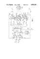
- FIG. 1 is an overall block diagram of a reconfigurable processing unit in accordance with the invention.
- FIG. 2 is a block diagram of a register portion of the register file of FIG. 1.
- 16-bit data or signals are applied from a source (not illustrated) to a first 16-bit input port 10 and further 16-bit signals are applied to a second 16-bit input port 12.
- Ports 10 and 12 are adaptable for receiving two single-precision 16-bit words, a single 32-bitdouble-precision word or a floating-point 24-bit mantissa together with 8-bit exponent.
- input signal is a 32-bit word
- input port 10 receives the more significant portion and input 12 receives the less significant portion.
- input port 10 receives the 16 most significant bits of the mantissa
- input port 12 receives the remaining 8 least significant bits of the mantissa in its eight most significant positions and the 8-bit exponent portion in its eight least significant portions. If only a single 16-bit word is to be processed, thesignal at input port 12 becomes irrelevant and is not loaded into the register file described below.
- the signal applied to input port 10 is applied over a 16-bit conductor set 14 to a first input port 16 of a multiplexer 18.
- the signal applied to input port 12 is applied over a conductor set 20 to a first input port 22 of a multiplexer 24.
- Multiplexers 18 and 24 are controlled from a multiplex control circuit 26.
- the signals applied by way of input ports 10 and 12 to input terminals 16 and 22 of multiplexers 18 and 24, respectively, are coupled from output ports of multiplexers 18 and 24 by way of conductor sets 28 and 30, respectively, to input terminals 32 and 34, respectively, of a register file 36.
- Register file 36 is grouping of registers, further described in conjunction with FIG. 2.
- Register file 36 stores words applied to input terminals 32 and 34 under control of steering control signals applied over a conductor set 120.
- Register file 36 is effectively a random-access memory which provides temporary storage to facilitate the operations of the arithmetic logic units (ALUs) described below.
- Register file 36 has 16-bit outputs at each of ports 38, 40, 42 and 44.
- Signals appearing at 16-bit output port 38 of register file 36 are applied over a conductor set 46 to the 16-bit first input port 48 of a 16-bit ALU 50.
- Signals appearing at output port 40 of register file 36 are applied over 16-bit conductor set 52 to a 16-bit input port 54 of ALU 50.
- the 16-bit MSB of a floating-point mantissa are applied to the input portsof ALU 50.
- Output signals appearing at 16-bit output port 42 of register file 36 are divided into most significant bit (MSB) and least significant bit (LSB) portions. The MSB portions are applied over an 8-conductor set 56 to a first 8-bit input port 58 of an 8-bit ALU 60.
- the LSB portions of the signal appearing at output port 42 of register file 36 are applied over an 8-conductor set 62 to a first 8-bit input port 64 of an 8-bit ALU 66.
- the 16-bit signals appearing at output port 44 of register file 36 aredivided into MSB and LSB portions, with the MSB portions being applied overan 8-conductor set 68 to a second 8-bit input port 70 of ALU 60, and the LSB being applied over an 8-conductor set 72 to a second 8-bit input port 74 of ALU 66.
- the eight least significant bits of the mantissa of a floating-point word are applied to the input ports of ALU 60, while the 8-bit mantissa bits are applied to the input ports of ALU 66.
- Eight-bit ALU 66 also includes a carry output port 76 which is coupled by way of a controllable switch 78 to a carry input port 80 of ALU 60. While switch 78 is illustrated as a mechanical single-pole, double-throw switch,those of ordinary skill in the art know that solid-state equivalents are used in practice.
- ALU 60 also includes a carry output port 82 which is coupled by way of a controllable switch 84 to a carry input pot 86 of ALU 50.
- Switch 78 in the position illustrated couples carry output terminal 76of ALU 66 to carry input terminal 80 of ALU 60, but in its alternate position (not illustrated) switch 78 decouples carry output terminal 76 from carry input terminal 80 and instead couples carry input terminal 80 to a terminal 88 to which logic low level (illustrated as ground) is applied.
- controllable switch 84 in the position illustrated couples carry output terminal 82 of ALU 60 to carry input terminal 86 of ALU 50, but in its alternate position (not illustrated) decouples them andinstead couples carry input port 86 to a logic low level (illustrated as ground) connected to a terminal 90.
- Switches 78 and 84 are controlled by aswitch control circuit illustrated as a block 92.
- Switch control circuit 92 may be a simple decoder which receives signals over a conductor set 93 representative of the type of signal being processed during the circuit clock cycle. Switch control circuit 92 decodes the signal and places switches 78 and 84 in the proper positions, as described below.
- Sixteen-bit ALU 50 produces its processed output signal at a 16-bit output port 94, which is coupled by a conductor set 96 to a second input port 98 of multiplexer 18.
- the signal produced by 8-bit ALU 60 is produced at an 8-bit output port 98 and is coupled to an MSB 8-conductor set 100.
- the 8-bit output signal of ALU 66 is produced at an 8-bit output port 102 and is coupled onto an LSB 8-conductor set 104.
- Conductor sets 100 and 104 merge to form a 16-conductor set 106 which is coupled to a second input port 108 of multiplexer 24.
- 32-bit bit operation is accomplished in three clock cycles.
- the first clock cycle is used to load the first 32-bit word into the register file from input ports 10 and 12, and the second clock cycle is used to load the second 32-bit word into the register file.
- the third clock cycle can be used for processing the words by the three ALUs 50, 60 and 66, connected as one 32-bit ALU by the illustrated position of switches 78 and 80.
- the processed words can be recirculated to register file 36 for further processing by way of the second inputs of multiplexers18 and 24.
- the 32-bit output can conveniently be taken from conductor sets 96 and 106, as illustrated by dashed lines 110 and 112 connected to 16-bit output ports 111 and 113, respectively.
- the first independent 16-bit input word is applied to input terminal 10 concurrently with application of the second independent 16-bit input word to input port 12, and the two words are stored simultaneously in register file 36 in response to the first clock cycle.
- 16-bit ALU 50 may process the data independently of ALUs 60 and 66, or 8-bit ALUs60 and 66 may process the signal together independently of ALU 50.
- Independence of ALU 50 from ALUs 60 and 66 in accomplished by throwing switch 84 to its open position, i.e. to the alternate position (not illustrated), in which terminal 86 is coupled to ground.
- Processing of four 16-bit single-precision words may be accomplished by (a)during a first clock cycle applying the first of two 16-bit words to register file 36 by way of input port 10 and multiplexer 18, and the second by input port 12 and multiplexer 24, and (b) during a second clock cycle applying a third 16-bit word to register file 36 by way of port 10 and multiplexer 18, and a fourth 16-bit word by way of port 12 and multiplexer 24.
- ALU 50 independently processes the first and third 16-bit words applied to its first (48) and second (54)input ports from ports 38 and 40 of register file 36, and ALUs 60 and 66 together independently process the second and fourth 16-bit works applied to their inputs from output ports 42 and 44 of register file 36.
- continuous operation includes loading and processing during each clock cycle.
- Switch 84 may be opened at any time prior to or at the time that the outputproduced at output port 94 (or 98, 102) is applied to a storage element, asfor example by recirculation through multiplexer 18 to register file 36, orapplication of an output by way of conductor set 110 to a utilization apparatus.
- 16-bit ALU 50 operates independently of ALUs 60 and 66.
- switch 78 With switch 78 closed, however, the carry output of ALU 66 is coupled to the carry input 80 of ALU 60, whereby the two 8-bit ALUs together form a single 16-bit ALU which is independent of 16-bit ALU 50.
- the 16-bit signal originally applied by way of input port 12and multiplexer 24 to register file 36 has its LSB portions processed by 8-bit ALU 86 and the MSB portions, together with the carry output of 8-bitALU 66, processed by 8-bit ALU 60.
- Two independent processed outputs are independently generated on conductor sets 96 and 106 and are available forrecirculation or for direct outputs as mentioned above.
- each symbol When performing operations on two 32-bit symbols, each in the form of a 24-bit mantissa together with an 8-bit exponent, each symbol is treated asan independent 32-bit word including 24-bit mantissa divided into first 16-bit MSB word and 8-bit LSB portion, with the 8-bit exponent associated with the 8-bit LSB mantissa portion in a second 16-bit word.
- the two resulting 16-bit words of each symbol are loaded into register 36 during one clock interval, whereupon loading of two such 32-bit symbols requires two clock cycles.
- the 24-bit mantissas are applied from ports 38, 40 and from the MSB portions of ports 42 and 44 of register file 36 to both inputports of 16-bit ALU 50 and to both input ports of 8-bit ALU 60.
- the 8-bit exponent is applied from the LSB portions of output ports 44 and 42 of register file 36 to both input ports 62 and 74 of 8-bit ALU 66.
- switch 84 is closed and switch 78 is opened. With switch 78 open, ALU 66 operates independently of the other two, and 8-bit ALU 60 acts in conjunction with 16-bit ALU 50 as a 24-bit ALU .
- the 24-bit mantissa portion of the symbols are processed by the 24-bit ALU combination, and the 8-bit mantissa portions are processed by 8-bit ALU 66.
- processing of the floating-point signal can be completed within one clock cycle, as with processing of simple 32-bit (double precision) and pairs of 16-bit (singleprecision) words.
- Switches 78 and 84 may be left open, thereby allowing independent operationof 16-bit ALU 50, 8-bit ALU 60 and 8-bit ALU 66 independent of each other.
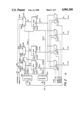
- FIG. 2 is a block diagram of register file 36. Elements of FIG. 2 corresponding to those of FIG. 1 are designated by the same reference numerals.
- 16-conductor set 28 is applied in parallel to 16-bit first input ports 208a, 208b . . . 208n of thirty-two multiplexers 210a, 210b . . . 210n, respectively.
- 16-conductor set 30 is applied in parallel to the 16-bit second input ports 206a, 206b . . . 206n of multiplexers 210a, 210b . . . 210n, respectively.
- the 16-bit output ports of multiplexers 210 are applied to 16-bit input ports of thirty-two 16-bitregisters 212a, 212b. . . 212n, respectively.
- the 16-bit word loaded into any one of registers 212 appears at all times on its 16-bit output conductor set 214a, 214b . . . 214n.
- the output conductor set 214 of each of registers 212 is applied simultaneously to one of the thirty-two 16-bitinput ports of each of multiplexers 216a, 216b, 216c and 216d.
- the 16-bit output conductor set of multiplexer 216a is coupled to 16-bit output port 38 of register file 36.
- the output of multiplexer 216b is coupled to 16-bit output port 40
- the output of multiplexer 216c is coupled to outputport 42
- the output of multiplexer 216d is coupled to output port 44.
- Each 32:1 multiplexer 216 is controlled by 5-bit control signals applied over a corresponding conductor set 218a-d, which is a portion of control conductor set 218.
- multiplexer 216a couples to its output conductor set and to output port 38the signal applied to a selected one of its thirty-two 16-bit inputs, underthe control of the 5-bit selection signal applied thereto over conductor set 218a.
- This arrangement allows the 16-bit word stored in any one of registers 212 to be coupled to any one of output ports 38, 40, 42 or 44, and allows simultaneous selection of the 16-bit words stored in any four of registers 212 for application to output ports 38-44.
- Each multiplexer 210 couples to its output conductor set and to the input port of the corresponding register 212 the signal applied to its first input port from conductor set 28 when its select (S) input terminal is in a particular logic state, as for example a logic low state. More specifically, when the S input of any multiplexer 210 is in a logic high condition, that multiplexer 210 couples to its output conductor set and tothe associated register 212 the signal applied to its second input port 206from conductor set 30. When the S input of a multiplexer 210 is at logic low level, that multiplexer couples to its output conductor set the signalapplied to its first input port from conductor set 28.
- Each register 212 includes a load enable (LE) input terminal.
- Each register212a, 212b . . . 212n is associated with an OR gate 220a, 220b . . . 220n, respectively.
- the output of each OR gate 220 is coupled to the LE input ofthe associated register 212.
- Each OR gate 220 includes two input terminals,one of which is connected to one of 32 single-conductor output conductors or lines 223 from a one-of-32 decoder 222.
- the other input terminal of each OR gate 220 is connected to one of the single-conductor output lines 225 of a second one-of-32 decoder 224.
- the 32 output conductors 225 of decoder 224 are applied individually to inputs of 32 separate OR gates 220.
- the output conductors 223 of decoder 222 are similarly connected to the second inputs of OR gates 220 and are also connected to the S inputs of the associated multiplexers 210.
- OR gate 220a has its output connected to the LE input terminal of register 212a, which is arranged to receive 16-bit signals from multiplexer 210a.
- An output conductor 223a from one-of-32 decoder 222 is connected to the S input of multiplexer 210a and to an input of OR gate 220a.
- OR gate 220a is also connected to one-of-32 decoders 224 output selection conductor 225a.
- Decoder 222 receives a 5-bit control signal from a conductor set 226, and decoder 224 receives a 5-bit control signal over a conductor set 228.
- the control signal applied to decoder 222 over conductor set 226 causes one ofits 31 output lines 223 to assume a logic high condition, thereby enabling one of the 31 registers 212 for writing into storage, and controlling the associated multiplexer 210 to couple the signal from conductor set 30 to that register for writing or loading.
- the next clock pulse causes writing into the register selected by decoder 222 of data from conductor set 30.
- the 5-bit control signal applied over conductor set 228 to decoder 224 can simultaneously select any other single register for loading from conductor set 28.
- the 5-bit signal on conductor set 228 causes one of the 32 output conductors 225 of decodes 224 to select a register 212 to be enabled by way of its associated OR gate 220. Since the output conductors of decoder 224 are notcoupled to the S input terminal of the associated multiplexers, the multiplexers associated with the registers 212 selected by decoder 224 couple to the selected register signals originating from conductor set 28.
- the same clock pulse which causes clocking into the register selected by decoder 222 also causes clocking into the register selected by decoder 224.
- a simple way of viewing this portion of the operation is to consider that a signal applied to conductor set 226 selects a register to be loaded(at the next clock pulse) from conductor set 30, and a signal applied to conductor set 228 selects a register to be similarly loaded from conductorset 28.
- switches 78 and 84 (FIG. 1) will depend uponthe types of data being processed from moment to moment, which as describedabove may be either single precision, double precision or floating-point ina particular clock cycle and will also depend upon the type of processing being accomplished. The control will be apparent to those of ordinary skill in the art, as will the control signals applied over conductor set 120 to cause the signals to arrive at the proper ports of the ALU. Similarly, the control of multiplexers 18 and 24 depends upon when new words are to be loaded, and whether recirculation of data is required, which depends upon the particular application of the arrangement.
- system output may be taken from output ports 38, 40, 42 and 44 of the register file instead of by way of output conductors 110,112 (FIG. 1).
- N 1 +N 2 +N 3 bit words where N 2 is the difference between N 1 and N 3 .
Abstract
Description
Claims (10)
Priority Applications (5)
| Application Number | Priority Date | Filing Date | Title |
|---|---|---|---|
| US07/234,124 US4901268A (en) | 1988-08-19 | 1988-08-19 | Multiple function data processor |
| CA000601486A CA1325281C (en) | 1988-08-19 | 1989-06-01 | Multiple function data processor |
| FR898910476A FR2635601B1 (en) | 1988-08-19 | 1989-08-03 | MULTIPURPOSE DATA PROCESSOR |
| GB8918917A GB2222012B (en) | 1988-08-19 | 1989-08-18 | Multiple function data processor |
| KR1019890011815A KR0137217B1 (en) | 1988-08-19 | 1989-08-19 | Multiple function data processor |
Applications Claiming Priority (1)
| Application Number | Priority Date | Filing Date | Title |
|---|---|---|---|
| US07/234,124 US4901268A (en) | 1988-08-19 | 1988-08-19 | Multiple function data processor |
Publications (1)
| Publication Number | Publication Date |
|---|---|
| US4901268A true US4901268A (en) | 1990-02-13 |
Family
ID=22880035
Family Applications (1)
| Application Number | Title | Priority Date | Filing Date |
|---|---|---|---|
| US07/234,124 Expired - Fee Related US4901268A (en) | 1988-08-19 | 1988-08-19 | Multiple function data processor |
Country Status (5)
| Country | Link |
|---|---|
| US (1) | US4901268A (en) |
| KR (1) | KR0137217B1 (en) |
| CA (1) | CA1325281C (en) |
| FR (1) | FR2635601B1 (en) |
| GB (1) | GB2222012B (en) |
Cited By (61)
| Publication number | Priority date | Publication date | Assignee | Title |
|---|---|---|---|---|
| US5001662A (en) * | 1989-04-28 | 1991-03-19 | Apple Computer, Inc. | Method and apparatus for multi-gauge computation |
| US5423052A (en) * | 1992-04-01 | 1995-06-06 | Mitsubishi Denki Kabushiki Kaisha | Central processing unit with switchable carry and borrow flag |
| US5625713A (en) * | 1991-08-09 | 1997-04-29 | Ricoh Corporation | Apparatus and method for increasing the throughput of an acoustic or image compression system |
| US5636351A (en) * | 1993-11-23 | 1997-06-03 | Hewlett-Packard Company | Performance of an operation on whole word operands and on operations in parallel on sub-word operands in a single processor |
| US5666510A (en) * | 1991-05-08 | 1997-09-09 | Hitachi, Ltd. | Data processing device having an expandable address space |
| US5757685A (en) * | 1992-08-31 | 1998-05-26 | Nec Corporation | Data processing system capable of processing long word data |
| US5787307A (en) * | 1994-11-18 | 1998-07-28 | International Business Machines Corporation | Apparatus for draining off electric charges from a bus connector pins having a switch controller for controlling two switches where the second switch connects the pins to ground |
| US5943242A (en) * | 1995-11-17 | 1999-08-24 | Pact Gmbh | Dynamically reconfigurable data processing system |
| US6021490A (en) * | 1996-12-20 | 2000-02-01 | Pact Gmbh | Run-time reconfiguration method for programmable units |
| US6032170A (en) * | 1993-11-30 | 2000-02-29 | Texas Instruments Incorporated | Long instruction word controlling plural independent processor operations |
| US6038650A (en) * | 1997-02-04 | 2000-03-14 | Pactgmbh | Method for the automatic address generation of modules within clusters comprised of a plurality of these modules |
| US6081903A (en) * | 1997-02-08 | 2000-06-27 | Pact Gmbh | Method of the self-synchronization of configurable elements of a programmable unit |
| US6088795A (en) * | 1996-12-27 | 2000-07-11 | Pact Gmbh | Process for automatic dynamic reloading of data flow processors (DFPs) and units with two or three-dimensional programmable cell architectures (FPGAs, DPGAs and the like) |
| US6119181A (en) * | 1996-12-20 | 2000-09-12 | Pact Gmbh | I/O and memory bus system for DFPs and units with two- or multi-dimensional programmable cell architectures |
| EP1055997A1 (en) * | 1999-05-21 | 2000-11-29 | Hewlett-Packard Company | A floating-point unit which utilizes standard MAC units for performing SIMD operations |
| US6338106B1 (en) | 1996-12-20 | 2002-01-08 | Pact Gmbh | I/O and memory bus system for DFPS and units with two or multi-dimensional programmable cell architectures |
| US6339800B1 (en) * | 1997-12-30 | 2002-01-15 | Hyundai Electronics Industries | Method for transmitting data between a microprocessor and an external memory module by using combined serial/parallel process |
| US6405299B1 (en) | 1997-02-11 | 2002-06-11 | Pact Gmbh | Internal bus system for DFPS and units with two- or multi-dimensional programmable cell architectures, for managing large volumes of data with a high interconnection complexity |
| US6425068B1 (en) | 1996-12-09 | 2002-07-23 | Pact Gmbh | Unit for processing numeric and logic operations for use in central processing units (cpus), multiprocessor systems, data-flow processors (dsps), systolic processors and field programmable gate arrays (epgas) |
| US6480937B1 (en) | 1998-02-25 | 2002-11-12 | Pact Informationstechnologie Gmbh | Method for hierarchical caching of configuration data having dataflow processors and modules having two-or multidimensional programmable cell structure (FPGAs, DPGAs, etc.)-- |
| US20030037085A1 (en) * | 2001-08-20 | 2003-02-20 | Sandbote Sam B. | Field processing unit |
| US20030046607A1 (en) * | 2001-09-03 | 2003-03-06 | Frank May | Method for debugging reconfigurable architectures |
| US6542998B1 (en) | 1997-02-08 | 2003-04-01 | Pact Gmbh | Method of self-synchronization of configurable elements of a programmable module |
| US20040015899A1 (en) * | 2000-10-06 | 2004-01-22 | Frank May | Method for processing data |
| US6697979B1 (en) | 1997-12-22 | 2004-02-24 | Pact Xpp Technologies Ag | Method of repairing integrated circuits |
| US20040153608A1 (en) * | 2001-01-09 | 2004-08-05 | Martin Vorbach | Method of hierarchical caching of configuration data having dataflow processors and modules having two- or multidimensional programmable cell structure (FPGAs, DPGAs, etc.) |
| US20040243984A1 (en) * | 2001-06-20 | 2004-12-02 | Martin Vorbach | Data processing method |
| US20040249880A1 (en) * | 2001-12-14 | 2004-12-09 | Martin Vorbach | Reconfigurable system |
| US20050053056A1 (en) * | 2001-09-03 | 2005-03-10 | Martin Vorbach | Router |
| US20050066213A1 (en) * | 2001-03-05 | 2005-03-24 | Martin Vorbach | Methods and devices for treating and processing data |
| US20050132344A1 (en) * | 2002-01-18 | 2005-06-16 | Martin Vorbach | Method of compilation |
| US20050223212A1 (en) * | 2000-06-13 | 2005-10-06 | Martin Vorbach | Pipeline configuration protocol and configuration unit communication |
| US20060031595A1 (en) * | 1996-12-27 | 2006-02-09 | Martin Vorbach | Process for automatic dynamic reloading of data flow processors (DFPs) and units with two- or three-dimensional programmable cell architectures (FPGAs, DPGAs, and the like |
| US20060075211A1 (en) * | 2002-03-21 | 2006-04-06 | Martin Vorbach | Method and device for data processing |
| US20060090062A1 (en) * | 2002-01-19 | 2006-04-27 | Martin Vorbach | Reconfigurable processor |
| US20060192586A1 (en) * | 2002-09-06 | 2006-08-31 | Martin Vorbach | Reconfigurable sequencer structure |
| US20060248317A1 (en) * | 2002-08-07 | 2006-11-02 | Martin Vorbach | Method and device for processing data |
| US20070011433A1 (en) * | 2003-04-04 | 2007-01-11 | Martin Vorbach | Method and device for data processing |
| US20070083730A1 (en) * | 2003-06-17 | 2007-04-12 | Martin Vorbach | Data processing device and method |
| US7210129B2 (en) | 2001-08-16 | 2007-04-24 | Pact Xpp Technologies Ag | Method for translating programs for reconfigurable architectures |
| US20070113046A1 (en) * | 2001-03-05 | 2007-05-17 | Martin Vorbach | Data processing device and method |
| US20070123091A1 (en) * | 2005-11-18 | 2007-05-31 | Swedberg Benjamin D | Releasable Wire Connector |
| US20070230336A1 (en) * | 2006-03-10 | 2007-10-04 | Fujitsu Limited | Reconfigurable circuit |
| US20090031104A1 (en) * | 2005-02-07 | 2009-01-29 | Martin Vorbach | Low Latency Massive Parallel Data Processing Device |
| US20090146691A1 (en) * | 2000-10-06 | 2009-06-11 | Martin Vorbach | Logic cell array and bus system |
| US20090172351A1 (en) * | 2003-08-28 | 2009-07-02 | Martin Vorbach | Data processing device and method |
| US20090210653A1 (en) * | 2001-03-05 | 2009-08-20 | Pact Xpp Technologies Ag | Method and device for treating and processing data |
| US7581076B2 (en) | 2001-03-05 | 2009-08-25 | Pact Xpp Technologies Ag | Methods and devices for treating and/or processing data |
| US7595659B2 (en) | 2000-10-09 | 2009-09-29 | Pact Xpp Technologies Ag | Logic cell array and bus system |
| US20090300262A1 (en) * | 2001-03-05 | 2009-12-03 | Martin Vorbach | Methods and devices for treating and/or processing data |
| US20100153654A1 (en) * | 2002-08-07 | 2010-06-17 | Martin Vorbach | Data processing method and device |
| US20100228918A1 (en) * | 1999-06-10 | 2010-09-09 | Martin Vorbach | Configurable logic integrated circuit having a multidimensional structure of configurable elements |
| US20100272811A1 (en) * | 2008-07-23 | 2010-10-28 | Alkermes,Inc. | Complex of trospium and pharmaceutical compositions thereof |
| US20110060942A1 (en) * | 2001-03-05 | 2011-03-10 | Martin Vorbach | Methods and devices for treating and/or processing data |
| US7996827B2 (en) | 2001-08-16 | 2011-08-09 | Martin Vorbach | Method for the translation of programs for reconfigurable architectures |
| US20110238948A1 (en) * | 2002-08-07 | 2011-09-29 | Martin Vorbach | Method and device for coupling a data processing unit and a data processing array |
| US8127061B2 (en) | 2002-02-18 | 2012-02-28 | Martin Vorbach | Bus systems and reconfiguration methods |
| US8156284B2 (en) | 2002-08-07 | 2012-04-10 | Martin Vorbach | Data processing method and device |
| US8250503B2 (en) | 2006-01-18 | 2012-08-21 | Martin Vorbach | Hardware definition method including determining whether to implement a function as hardware or software |
| US8686475B2 (en) | 2001-09-19 | 2014-04-01 | Pact Xpp Technologies Ag | Reconfigurable elements |
| US8686549B2 (en) | 2001-09-03 | 2014-04-01 | Martin Vorbach | Reconfigurable elements |
Families Citing this family (2)
| Publication number | Priority date | Publication date | Assignee | Title |
|---|---|---|---|---|
| JP2651267B2 (en) * | 1990-07-26 | 1997-09-10 | 富士通株式会社 | Arithmetic processing device and arithmetic processing method |
| EP1120193A4 (en) * | 1998-10-30 | 2002-07-24 | Shinetsu Handotai Kk | Unpolished work holding board and production method thereof and work polishing method and device |
Citations (7)
| Publication number | Priority date | Publication date | Assignee | Title |
|---|---|---|---|---|
| US4722068A (en) * | 1984-04-26 | 1988-01-26 | Nec Corporation | Double precision multiplier |
| US4752901A (en) * | 1985-09-16 | 1988-06-21 | Motorola, Inc. | Arithmetic logic unit utilizing strobed gates |
| US4754412A (en) * | 1985-10-07 | 1988-06-28 | Schlumberger Systems & Services, Inc. | Arithmetic logic system using the output of a first alu to control the operation of a second alu |
| US4760544A (en) * | 1986-06-20 | 1988-07-26 | Plessey Overseas Limited | Arithmetic logic and shift device |
| US4760551A (en) * | 1984-12-14 | 1988-07-26 | Goichi Yokomizo | Operation unit for floating point data with variable exponent-part length |
| US4768160A (en) * | 1985-04-16 | 1988-08-30 | Nec Corporation | Arithmetic unit with simple overflow detection system |
| US4823260A (en) * | 1987-11-12 | 1989-04-18 | Intel Corporation | Mixed-precision floating point operations from a single instruction opcode |
Family Cites Families (6)
| Publication number | Priority date | Publication date | Assignee | Title |
|---|---|---|---|---|
| US4161784A (en) * | 1978-01-05 | 1979-07-17 | Honeywell Information Systems, Inc. | Microprogrammable floating point arithmetic unit capable of performing arithmetic operations on long and short operands |
| US4296469A (en) * | 1978-11-17 | 1981-10-20 | Motorola, Inc. | Execution unit for data processor using segmented bus structure |
| US4612628A (en) * | 1983-02-14 | 1986-09-16 | Data General Corp. | Floating-point unit constructed of identical modules |
| JPS61255433A (en) * | 1985-05-07 | 1986-11-13 | Mitsubishi Electric Corp | Arithmetic unit |
| US4748585A (en) * | 1985-12-26 | 1988-05-31 | Chiarulli Donald M | Processor utilizing reconfigurable process segments to accomodate data word length |
| DE3770353D1 (en) * | 1986-07-11 | 1991-07-04 | Siemens Ag | METHOD AND ARRANGEMENT FOR LINKING OPERANDS OF VARIABLE LENGTH IN DATA PROCESSING SYSTEMS. |
-
1988
- 1988-08-19 US US07/234,124 patent/US4901268A/en not_active Expired - Fee Related
-
1989
- 1989-06-01 CA CA000601486A patent/CA1325281C/en not_active Expired - Fee Related
- 1989-08-03 FR FR898910476A patent/FR2635601B1/en not_active Expired - Fee Related
- 1989-08-18 GB GB8918917A patent/GB2222012B/en not_active Expired - Fee Related
- 1989-08-19 KR KR1019890011815A patent/KR0137217B1/en not_active IP Right Cessation
Patent Citations (7)
| Publication number | Priority date | Publication date | Assignee | Title |
|---|---|---|---|---|
| US4722068A (en) * | 1984-04-26 | 1988-01-26 | Nec Corporation | Double precision multiplier |
| US4760551A (en) * | 1984-12-14 | 1988-07-26 | Goichi Yokomizo | Operation unit for floating point data with variable exponent-part length |
| US4768160A (en) * | 1985-04-16 | 1988-08-30 | Nec Corporation | Arithmetic unit with simple overflow detection system |
| US4752901A (en) * | 1985-09-16 | 1988-06-21 | Motorola, Inc. | Arithmetic logic unit utilizing strobed gates |
| US4754412A (en) * | 1985-10-07 | 1988-06-28 | Schlumberger Systems & Services, Inc. | Arithmetic logic system using the output of a first alu to control the operation of a second alu |
| US4760544A (en) * | 1986-06-20 | 1988-07-26 | Plessey Overseas Limited | Arithmetic logic and shift device |
| US4823260A (en) * | 1987-11-12 | 1989-04-18 | Intel Corporation | Mixed-precision floating point operations from a single instruction opcode |
Cited By (159)
| Publication number | Priority date | Publication date | Assignee | Title |
|---|---|---|---|---|
| US5001662A (en) * | 1989-04-28 | 1991-03-19 | Apple Computer, Inc. | Method and apparatus for multi-gauge computation |
| US5666510A (en) * | 1991-05-08 | 1997-09-09 | Hitachi, Ltd. | Data processing device having an expandable address space |
| US5625713A (en) * | 1991-08-09 | 1997-04-29 | Ricoh Corporation | Apparatus and method for increasing the throughput of an acoustic or image compression system |
| US5423052A (en) * | 1992-04-01 | 1995-06-06 | Mitsubishi Denki Kabushiki Kaisha | Central processing unit with switchable carry and borrow flag |
| US5757685A (en) * | 1992-08-31 | 1998-05-26 | Nec Corporation | Data processing system capable of processing long word data |
| US5636351A (en) * | 1993-11-23 | 1997-06-03 | Hewlett-Packard Company | Performance of an operation on whole word operands and on operations in parallel on sub-word operands in a single processor |
| US6032170A (en) * | 1993-11-30 | 2000-02-29 | Texas Instruments Incorporated | Long instruction word controlling plural independent processor operations |
| US5787307A (en) * | 1994-11-18 | 1998-07-28 | International Business Machines Corporation | Apparatus for draining off electric charges from a bus connector pins having a switch controller for controlling two switches where the second switch connects the pins to ground |
| US5943242A (en) * | 1995-11-17 | 1999-08-24 | Pact Gmbh | Dynamically reconfigurable data processing system |
| US6859869B1 (en) | 1995-11-17 | 2005-02-22 | Pact Xpp Technologies Ag | Data processing system |
| US7822968B2 (en) | 1996-12-09 | 2010-10-26 | Martin Vorbach | Circuit having a multidimensional structure of configurable cells that include multi-bit-wide inputs and outputs |
| US6728871B1 (en) | 1996-12-09 | 2004-04-27 | Pact Xpp Technologies Ag | Runtime configurable arithmetic and logic cell |
| US7237087B2 (en) | 1996-12-09 | 2007-06-26 | Pact Xpp Technologies Ag | Reconfigurable multidimensional array processor allowing runtime reconfiguration of selected individual array cells |
| US20110010523A1 (en) * | 1996-12-09 | 2011-01-13 | Martin Vorbach | Runtime configurable arithmetic and logic cell |
| US20090146690A1 (en) * | 1996-12-09 | 2009-06-11 | Martin Vorbach | Runtime configurable arithmetic and logic cell |
| US7565525B2 (en) | 1996-12-09 | 2009-07-21 | Pact Xpp Technologies Ag | Runtime configurable arithmetic and logic cell |
| US8156312B2 (en) | 1996-12-09 | 2012-04-10 | Martin Vorbach | Processor chip for reconfigurable data processing, for processing numeric and logic operations and including function and interconnection control units |
| US20080010437A1 (en) * | 1996-12-09 | 2008-01-10 | Martin Vorbach | Unit for processing numeric and logic operations for use in central processing units (CPUS), multiprocessor systems, data-flow processors (DSPS), systolic processors and field programmable gate arrays (FPGAS) |
| US6425068B1 (en) | 1996-12-09 | 2002-07-23 | Pact Gmbh | Unit for processing numeric and logic operations for use in central processing units (cpus), multiprocessor systems, data-flow processors (dsps), systolic processors and field programmable gate arrays (epgas) |
| US20040168099A1 (en) * | 1996-12-09 | 2004-08-26 | Martin Vorbach | Unit for processing numeric and logic operations for use in central processing units (CPUs), multiprocessor systems |
| US20100287318A1 (en) * | 1996-12-20 | 2010-11-11 | Martin Vorbach | I/o and memory bus system for dfps and units with two- or multi-dimensional programmable cell architectures |
| US6513077B2 (en) | 1996-12-20 | 2003-01-28 | Pact Gmbh | I/O and memory bus system for DFPs and units with two- or multi-dimensional programmable cell architectures |
| US7899962B2 (en) | 1996-12-20 | 2011-03-01 | Martin Vorbach | I/O and memory bus system for DFPs and units with two- or multi-dimensional programmable cell architectures |
| US20100082863A1 (en) * | 1996-12-20 | 2010-04-01 | Martin Vorbach | I/O AND MEMORY BUS SYSTEM FOR DFPs AND UNITS WITH TWO- OR MULTI-DIMENSIONAL PROGRAMMABLE CELL ARCHITECTURES |
| US7650448B2 (en) | 1996-12-20 | 2010-01-19 | Pact Xpp Technologies Ag | I/O and memory bus system for DFPS and units with two- or multi-dimensional programmable cell architectures |
| US7337249B2 (en) | 1996-12-20 | 2008-02-26 | Pact Xpp Technologies Ag | I/O and memory bus system for DFPS and units with two- or multi-dimensional programmable cell architectures |
| US6338106B1 (en) | 1996-12-20 | 2002-01-08 | Pact Gmbh | I/O and memory bus system for DFPS and units with two or multi-dimensional programmable cell architectures |
| US8195856B2 (en) | 1996-12-20 | 2012-06-05 | Martin Vorbach | I/O and memory bus system for DFPS and units with two- or multi-dimensional programmable cell architectures |
| US7243175B2 (en) | 1996-12-20 | 2007-07-10 | Pact Xpp Technologies Ag | I/O and memory bus system for DFPs and units with two-or multi-dimensional programmable cell architectures |
| US20040199688A1 (en) * | 1996-12-20 | 2004-10-07 | Martin Vorbach | I/O and memory bus system for DFPs and units with two-or multi-dimensional programmable cell architectures |
| US6119181A (en) * | 1996-12-20 | 2000-09-12 | Pact Gmbh | I/O and memory bus system for DFPs and units with two- or multi-dimensional programmable cell architectures |
| US20080222329A1 (en) * | 1996-12-20 | 2008-09-11 | Martin Vorbach | I/O and memory bus system for DFPs and units with two- or multi-dimensional programmable cell architectures |
| US6721830B2 (en) | 1996-12-20 | 2004-04-13 | Pact Xpp Technologies Ag | I/O and memory bus system for DFPs and units with two- or multi-dimensional programmable cell architectures |
| US7174443B1 (en) | 1996-12-20 | 2007-02-06 | Pact Xpp Technologies Ag | Run-time reconfiguration method for programmable units |
| US6021490A (en) * | 1996-12-20 | 2000-02-01 | Pact Gmbh | Run-time reconfiguration method for programmable units |
| US6088795A (en) * | 1996-12-27 | 2000-07-11 | Pact Gmbh | Process for automatic dynamic reloading of data flow processors (DFPs) and units with two or three-dimensional programmable cell architectures (FPGAs, DPGAs and the like) |
| US6477643B1 (en) | 1996-12-27 | 2002-11-05 | Pact Gmbh | Process for automatic dynamic reloading of data flow processors (dfps) and units with two-or-three-dimensional programmable cell architectures (fpgas, dpgas, and the like) |
| US20090144485A1 (en) * | 1996-12-27 | 2009-06-04 | Martin Vorbach | Process for automatic dynamic reloading of data flow processors (dfps) and units with two- or three-dimensional programmable cell architectures (fpgas, dpgas, and the like) |
| US20090153188A1 (en) * | 1996-12-27 | 2009-06-18 | Martin Vorbach | PROCESS FOR AUTOMATIC DYNAMIC RELOADING OF DATA FLOW PROCESSORS (DFPs) AND UNITS WITH TWO- OR THREE-DIMENSIONAL PROGRAMMABLE CELL ARCHITECTURES (FPGAs, DPGAs AND THE LIKE) |
| US20060031595A1 (en) * | 1996-12-27 | 2006-02-09 | Martin Vorbach | Process for automatic dynamic reloading of data flow processors (DFPs) and units with two- or three-dimensional programmable cell architectures (FPGAs, DPGAs, and the like |
| US7822881B2 (en) | 1996-12-27 | 2010-10-26 | Martin Vorbach | Process for automatic dynamic reloading of data flow processors (DFPs) and units with two- or three-dimensional programmable cell architectures (FPGAs, DPGAs, and the like) |
| US6038650A (en) * | 1997-02-04 | 2000-03-14 | Pactgmbh | Method for the automatic address generation of modules within clusters comprised of a plurality of these modules |
| US6542998B1 (en) | 1997-02-08 | 2003-04-01 | Pact Gmbh | Method of self-synchronization of configurable elements of a programmable module |
| USRE45223E1 (en) | 1997-02-08 | 2014-10-28 | Pact Xpp Technologies Ag | Method of self-synchronization of configurable elements of a programmable module |
| US6526520B1 (en) | 1997-02-08 | 2003-02-25 | Pact Gmbh | Method of self-synchronization of configurable elements of a programmable unit |
| USRE45109E1 (en) | 1997-02-08 | 2014-09-02 | Pact Xpp Technologies Ag | Method of self-synchronization of configurable elements of a programmable module |
| US6081903A (en) * | 1997-02-08 | 2000-06-27 | Pact Gmbh | Method of the self-synchronization of configurable elements of a programmable unit |
| USRE44365E1 (en) | 1997-02-08 | 2013-07-09 | Martin Vorbach | Method of self-synchronization of configurable elements of a programmable module |
| US6968452B2 (en) | 1997-02-08 | 2005-11-22 | Pact Xpp Technologies Ag | Method of self-synchronization of configurable elements of a programmable unit |
| USRE44383E1 (en) | 1997-02-08 | 2013-07-16 | Martin Vorbach | Method of self-synchronization of configurable elements of a programmable module |
| US20040083399A1 (en) * | 1997-02-08 | 2004-04-29 | Martin Vorbach | Method of self-synchronization of configurable elements of a programmable module |
| US7036036B2 (en) | 1997-02-08 | 2006-04-25 | Pact Xpp Technologies Ag | Method of self-synchronization of configurable elements of a programmable module |
| US20040052130A1 (en) * | 1997-02-08 | 2004-03-18 | Martin Vorbach | Method of self-synchronization of configurable elements of a programmable unit |
| US7010667B2 (en) * | 1997-02-11 | 2006-03-07 | Pact Xpp Technologies Ag | Internal bus system for DFPS and units with two- or multi-dimensional programmable cell architectures, for managing large volumes of data with a high interconnection complexity |
| US20030135686A1 (en) * | 1997-02-11 | 2003-07-17 | Martin Vorbach | Internal bus system for DFPs and units with two- or multi-dimensional programmable cell architectures, for managing large volumes of data with a high interconnection complexity |
| US6405299B1 (en) | 1997-02-11 | 2002-06-11 | Pact Gmbh | Internal bus system for DFPS and units with two- or multi-dimensional programmable cell architectures, for managing large volumes of data with a high interconnection complexity |
| US8819505B2 (en) | 1997-12-22 | 2014-08-26 | Pact Xpp Technologies Ag | Data processor having disabled cores |
| US6697979B1 (en) | 1997-12-22 | 2004-02-24 | Pact Xpp Technologies Ag | Method of repairing integrated circuits |
| US20040181726A1 (en) * | 1997-12-22 | 2004-09-16 | Martin Vorbach | Method and system for alternating between programs for execution by cells of an integrated circuit |
| US20090300445A1 (en) * | 1997-12-22 | 2009-12-03 | Martin Vorbach | Method and system for alternating between programs for execution by cells of an integrated circuit |
| US6339800B1 (en) * | 1997-12-30 | 2002-01-15 | Hyundai Electronics Industries | Method for transmitting data between a microprocessor and an external memory module by using combined serial/parallel process |
| US6687788B2 (en) | 1998-02-25 | 2004-02-03 | Pact Xpp Technologies Ag | Method of hierarchical caching of configuration data having dataflow processors and modules having two-or multidimensional programmable cell structure (FPGAs, DPGAs , etc.) |
| US6571381B1 (en) | 1998-02-25 | 2003-05-27 | Pact Xpp Technologies Ag | Method for deadlock-free configuration of dataflow processors and modules with a two- or multidimensional programmable cell structure (FPGAs, DPGAs, etc.) |
| US6480937B1 (en) | 1998-02-25 | 2002-11-12 | Pact Informationstechnologie Gmbh | Method for hierarchical caching of configuration data having dataflow processors and modules having two-or multidimensional programmable cell structure (FPGAs, DPGAs, etc.)-- |
| US8468329B2 (en) | 1999-02-25 | 2013-06-18 | Martin Vorbach | Pipeline configuration protocol and configuration unit communication |
| EP1055997A1 (en) * | 1999-05-21 | 2000-11-29 | Hewlett-Packard Company | A floating-point unit which utilizes standard MAC units for performing SIMD operations |
| US20100228918A1 (en) * | 1999-06-10 | 2010-09-09 | Martin Vorbach | Configurable logic integrated circuit having a multidimensional structure of configurable elements |
| US8312200B2 (en) | 1999-06-10 | 2012-11-13 | Martin Vorbach | Processor chip including a plurality of cache elements connected to a plurality of processor cores |
| US8726250B2 (en) | 1999-06-10 | 2014-05-13 | Pact Xpp Technologies Ag | Configurable logic integrated circuit having a multidimensional structure of configurable elements |
| US8230411B1 (en) | 1999-06-10 | 2012-07-24 | Martin Vorbach | Method for interleaving a program over a plurality of cells |
| US20050223212A1 (en) * | 2000-06-13 | 2005-10-06 | Martin Vorbach | Pipeline configuration protocol and configuration unit communication |
| US8301872B2 (en) | 2000-06-13 | 2012-10-30 | Martin Vorbach | Pipeline configuration protocol and configuration unit communication |
| US7003660B2 (en) | 2000-06-13 | 2006-02-21 | Pact Xpp Technologies Ag | Pipeline configuration unit protocols and communication |
| US20090146691A1 (en) * | 2000-10-06 | 2009-06-11 | Martin Vorbach | Logic cell array and bus system |
| US8471593B2 (en) | 2000-10-06 | 2013-06-25 | Martin Vorbach | Logic cell array and bus system |
| US20040015899A1 (en) * | 2000-10-06 | 2004-01-22 | Frank May | Method for processing data |
| US9047440B2 (en) | 2000-10-06 | 2015-06-02 | Pact Xpp Technologies Ag | Logical cell array and bus system |
| US8058899B2 (en) | 2000-10-06 | 2011-11-15 | Martin Vorbach | Logic cell array and bus system |
| US7595659B2 (en) | 2000-10-09 | 2009-09-29 | Pact Xpp Technologies Ag | Logic cell array and bus system |
| US20040153608A1 (en) * | 2001-01-09 | 2004-08-05 | Martin Vorbach | Method of hierarchical caching of configuration data having dataflow processors and modules having two- or multidimensional programmable cell structure (FPGAs, DPGAs, etc.) |
| US20050257009A9 (en) * | 2001-01-09 | 2005-11-17 | Martin Vorbach | Method of hierarchical caching of configuration data having dataflow processors and modules having two- or multidimensional programmable cell structure (fpgas, dpgas, etc.) |
| US6990555B2 (en) | 2001-01-09 | 2006-01-24 | Pact Xpp Technologies Ag | Method of hierarchical caching of configuration data having dataflow processors and modules having two- or multidimensional programmable cell structure (FPGAs, DPGAs, etc.) |
| US20090100286A1 (en) * | 2001-03-05 | 2009-04-16 | Martin Vorbach | Methods and devices for treating and processing data |
| US9037807B2 (en) | 2001-03-05 | 2015-05-19 | Pact Xpp Technologies Ag | Processor arrangement on a chip including data processing, memory, and interface elements |
| US8099618B2 (en) | 2001-03-05 | 2012-01-17 | Martin Vorbach | Methods and devices for treating and processing data |
| US8145881B2 (en) | 2001-03-05 | 2012-03-27 | Martin Vorbach | Data processing device and method |
| US20070113046A1 (en) * | 2001-03-05 | 2007-05-17 | Martin Vorbach | Data processing device and method |
| US7444531B2 (en) | 2001-03-05 | 2008-10-28 | Pact Xpp Technologies Ag | Methods and devices for treating and processing data |
| US20110173389A1 (en) * | 2001-03-05 | 2011-07-14 | Martin Vorbach | Methods and devices for treating and/or processing data |
| US20090210653A1 (en) * | 2001-03-05 | 2009-08-20 | Pact Xpp Technologies Ag | Method and device for treating and processing data |
| US7581076B2 (en) | 2001-03-05 | 2009-08-25 | Pact Xpp Technologies Ag | Methods and devices for treating and/or processing data |
| US7844796B2 (en) | 2001-03-05 | 2010-11-30 | Martin Vorbach | Data processing device and method |
| US20110060942A1 (en) * | 2001-03-05 | 2011-03-10 | Martin Vorbach | Methods and devices for treating and/or processing data |
| US20090144522A1 (en) * | 2001-03-05 | 2009-06-04 | Martin Vorbach | Data Processing Device and Method |
| US20090300262A1 (en) * | 2001-03-05 | 2009-12-03 | Martin Vorbach | Methods and devices for treating and/or processing data |
| US9075605B2 (en) | 2001-03-05 | 2015-07-07 | Pact Xpp Technologies Ag | Methods and devices for treating and processing data |
| US20100023796A1 (en) * | 2001-03-05 | 2010-01-28 | Martin Vorbach | Methods and devices for treating and processing data |
| US20050066213A1 (en) * | 2001-03-05 | 2005-03-24 | Martin Vorbach | Methods and devices for treating and processing data |
| US8312301B2 (en) | 2001-03-05 | 2012-11-13 | Martin Vorbach | Methods and devices for treating and processing data |
| US7657877B2 (en) | 2001-06-20 | 2010-02-02 | Pact Xpp Technologies Ag | Method for processing data |
| US20100095094A1 (en) * | 2001-06-20 | 2010-04-15 | Martin Vorbach | Method for processing data |
| US20040243984A1 (en) * | 2001-06-20 | 2004-12-02 | Martin Vorbach | Data processing method |
| US8869121B2 (en) | 2001-08-16 | 2014-10-21 | Pact Xpp Technologies Ag | Method for the translation of programs for reconfigurable architectures |
| US7996827B2 (en) | 2001-08-16 | 2011-08-09 | Martin Vorbach | Method for the translation of programs for reconfigurable architectures |
| US7210129B2 (en) | 2001-08-16 | 2007-04-24 | Pact Xpp Technologies Ag | Method for translating programs for reconfigurable architectures |
| US20030037085A1 (en) * | 2001-08-20 | 2003-02-20 | Sandbote Sam B. | Field processing unit |
| US20090037865A1 (en) * | 2001-09-03 | 2009-02-05 | Martin Vorbach | Router |
| US8686549B2 (en) | 2001-09-03 | 2014-04-01 | Martin Vorbach | Reconfigurable elements |
| US20030046607A1 (en) * | 2001-09-03 | 2003-03-06 | Frank May | Method for debugging reconfigurable architectures |
| US7434191B2 (en) | 2001-09-03 | 2008-10-07 | Pact Xpp Technologies Ag | Router |
| US7480825B2 (en) | 2001-09-03 | 2009-01-20 | Pact Xpp Technologies Ag | Method for debugging reconfigurable architectures |
| US7840842B2 (en) | 2001-09-03 | 2010-11-23 | Martin Vorbach | Method for debugging reconfigurable architectures |
| US20050022062A1 (en) * | 2001-09-03 | 2005-01-27 | Martin Vorbach | Method for debugging reconfigurable architectures |
| US20050053056A1 (en) * | 2001-09-03 | 2005-03-10 | Martin Vorbach | Router |
| US7266725B2 (en) | 2001-09-03 | 2007-09-04 | Pact Xpp Technologies Ag | Method for debugging reconfigurable architectures |
| US8407525B2 (en) | 2001-09-03 | 2013-03-26 | Pact Xpp Technologies Ag | Method for debugging reconfigurable architectures |
| US8069373B2 (en) | 2001-09-03 | 2011-11-29 | Martin Vorbach | Method for debugging reconfigurable architectures |
| US8209653B2 (en) | 2001-09-03 | 2012-06-26 | Martin Vorbach | Router |
| US20090150725A1 (en) * | 2001-09-03 | 2009-06-11 | Martin Vorbach | Method for debugging reconfigurable architectures |
| US8429385B2 (en) | 2001-09-03 | 2013-04-23 | Martin Vorbach | Device including a field having function cells and information providing cells controlled by the function cells |
| US20060245225A1 (en) * | 2001-09-03 | 2006-11-02 | Martin Vorbach | Reconfigurable elements |
| US8686475B2 (en) | 2001-09-19 | 2014-04-01 | Pact Xpp Technologies Ag | Reconfigurable elements |
| US7577822B2 (en) | 2001-12-14 | 2009-08-18 | Pact Xpp Technologies Ag | Parallel task operation in processor and reconfigurable coprocessor configured based on information in link list including termination information for synchronization |
| US20040249880A1 (en) * | 2001-12-14 | 2004-12-09 | Martin Vorbach | Reconfigurable system |
| US20050132344A1 (en) * | 2002-01-18 | 2005-06-16 | Martin Vorbach | Method of compilation |
| US20060090062A1 (en) * | 2002-01-19 | 2006-04-27 | Martin Vorbach | Reconfigurable processor |
| US8281108B2 (en) | 2002-01-19 | 2012-10-02 | Martin Vorbach | Reconfigurable general purpose processor having time restricted configurations |
| US8127061B2 (en) | 2002-02-18 | 2012-02-28 | Martin Vorbach | Bus systems and reconfiguration methods |
| US20060075211A1 (en) * | 2002-03-21 | 2006-04-06 | Martin Vorbach | Method and device for data processing |
| US20100174868A1 (en) * | 2002-03-21 | 2010-07-08 | Martin Vorbach | Processor device having a sequential data processing unit and an arrangement of data processing elements |
| US20110238948A1 (en) * | 2002-08-07 | 2011-09-29 | Martin Vorbach | Method and device for coupling a data processing unit and a data processing array |
| US7657861B2 (en) | 2002-08-07 | 2010-02-02 | Pact Xpp Technologies Ag | Method and device for processing data |
| US20100153654A1 (en) * | 2002-08-07 | 2010-06-17 | Martin Vorbach | Data processing method and device |
| US8914590B2 (en) | 2002-08-07 | 2014-12-16 | Pact Xpp Technologies Ag | Data processing method and device |
| US8281265B2 (en) | 2002-08-07 | 2012-10-02 | Martin Vorbach | Method and device for processing data |
| US8156284B2 (en) | 2002-08-07 | 2012-04-10 | Martin Vorbach | Data processing method and device |
| US20100070671A1 (en) * | 2002-08-07 | 2010-03-18 | Martin Vorbach | Method and device for processing data |
| US20060248317A1 (en) * | 2002-08-07 | 2006-11-02 | Martin Vorbach | Method and device for processing data |
| US20060192586A1 (en) * | 2002-09-06 | 2006-08-31 | Martin Vorbach | Reconfigurable sequencer structure |
| US7782087B2 (en) | 2002-09-06 | 2010-08-24 | Martin Vorbach | Reconfigurable sequencer structure |
| US7394284B2 (en) | 2002-09-06 | 2008-07-01 | Pact Xpp Technologies Ag | Reconfigurable sequencer structure |
| US20110006805A1 (en) * | 2002-09-06 | 2011-01-13 | Martin Vorbach | Reconfigurable sequencer structure |
| US20080191737A1 (en) * | 2002-09-06 | 2008-08-14 | Martin Vorbach | Reconfigurable sequencer structure |
| US7602214B2 (en) | 2002-09-06 | 2009-10-13 | Pact Xpp Technologies Ag | Reconfigurable sequencer structure |
| US8803552B2 (en) | 2002-09-06 | 2014-08-12 | Pact Xpp Technologies Ag | Reconfigurable sequencer structure |
| US8310274B2 (en) | 2002-09-06 | 2012-11-13 | Martin Vorbach | Reconfigurable sequencer structure |
| US20110148460A1 (en) * | 2002-09-06 | 2011-06-23 | Martin Vorbach | Reconfigurable sequencer structure |
| US7928763B2 (en) | 2002-09-06 | 2011-04-19 | Martin Vorbach | Multi-core processing system |
| US20070011433A1 (en) * | 2003-04-04 | 2007-01-11 | Martin Vorbach | Method and device for data processing |
| US20070083730A1 (en) * | 2003-06-17 | 2007-04-12 | Martin Vorbach | Data processing device and method |
| US20090172351A1 (en) * | 2003-08-28 | 2009-07-02 | Martin Vorbach | Data processing device and method |
| US8812820B2 (en) | 2003-08-28 | 2014-08-19 | Pact Xpp Technologies Ag | Data processing device and method |
| US20100241823A1 (en) * | 2003-08-28 | 2010-09-23 | Martin Vorbach | Data processing device and method |
| US20090031104A1 (en) * | 2005-02-07 | 2009-01-29 | Martin Vorbach | Low Latency Massive Parallel Data Processing Device |
| US20070123091A1 (en) * | 2005-11-18 | 2007-05-31 | Swedberg Benjamin D | Releasable Wire Connector |
| US8250503B2 (en) | 2006-01-18 | 2012-08-21 | Martin Vorbach | Hardware definition method including determining whether to implement a function as hardware or software |
| US8099540B2 (en) * | 2006-03-10 | 2012-01-17 | Fujitsu Semiconductor Limited | Reconfigurable circuit |
| US20070230336A1 (en) * | 2006-03-10 | 2007-10-04 | Fujitsu Limited | Reconfigurable circuit |
| US20100272811A1 (en) * | 2008-07-23 | 2010-10-28 | Alkermes,Inc. | Complex of trospium and pharmaceutical compositions thereof |
Also Published As
| Publication number | Publication date |
|---|---|
| GB2222012A (en) | 1990-02-21 |
| CA1325281C (en) | 1993-12-14 |
| FR2635601B1 (en) | 1993-08-13 |
| KR900003733A (en) | 1990-03-26 |
| KR0137217B1 (en) | 1998-06-15 |
| GB8918917D0 (en) | 1989-09-27 |
| FR2635601A1 (en) | 1990-02-23 |
| GB2222012B (en) | 1992-09-09 |
Similar Documents
| Publication | Publication Date | Title |
|---|---|---|
| US4901268A (en) | Multiple function data processor | |
| US3537074A (en) | Parallel operating array computer | |
| US4577282A (en) | Microcomputer system for digital signal processing | |
| US5287532A (en) | Processor elements having multi-byte structure shift register for shifting data either byte wise or bit wise with single-bit output formed at bit positions thereof spaced by one byte | |
| US4491910A (en) | Microcomputer having data shift within memory | |
| EP0127988B1 (en) | A normalizing circuit | |
| US6009451A (en) | Method for generating barrel shifter result flags directly from input data | |
| US4713748A (en) | Microprocessor with block move instruction | |
| US4713749A (en) | Microprocessor with repeat instruction | |
| US4514805A (en) | Interrupt operation in systems emulator mode for microcomputer | |
| US4498135A (en) | Microcomputer with accumulator addressing | |
| US20040254965A1 (en) | Apparatus for variable word length computing in an array processor | |
| US4775952A (en) | Parallel processing system apparatus | |
| US4454589A (en) | Programmable arithmetic logic unit | |
| US3699326A (en) | Rounding numbers expressed in 2{40 s complement notation | |
| US4608634A (en) | Microcomputer with offset in store-accumulator operations | |
| US4528641A (en) | Variable radix processor | |
| EP0234495B1 (en) | Arithmetic circuit capable of executing floating point operations and fixed point operations | |
| US4533992A (en) | Microcomputer having shifter in ALU input | |
| US4586131A (en) | Microcomputer having data move circuits for within-memory shift of data words | |
| US4494187A (en) | Microcomputer with high speed program memory | |
| US4506322A (en) | Read/write memory cell for microcomputer | |
| US4644489A (en) | Multi-format binary coded decimal processor with selective output formatting | |
| US5432727A (en) | Apparatus for computing a sticky bit for a floating point arithmetic unit | |
| US5854907A (en) | Microcomputer for digital signal processing having on-chip memory and external memory access |
Legal Events
| Date | Code | Title | Description |
|---|---|---|---|
| AS | Assignment |
Owner name: GENERAL ELECTRIC COMPANY, A CORP. OF NEW YORK Free format text: ASSIGNMENT OF ASSIGNORS INTEREST.;ASSIGNOR:JUDD, JAMES E.;REEL/FRAME:004931/0389 Effective date: 19880815 Owner name: GENERAL ELECTRIC COMPANY, NEW YORK Free format text: ASSIGNMENT OF ASSIGNORS INTEREST;ASSIGNOR:JUDD, JAMES E.;REEL/FRAME:004931/0389 Effective date: 19880815 |
|
| FEPP | Fee payment procedure |
Free format text: PAYOR NUMBER ASSIGNED (ORIGINAL EVENT CODE: ASPN); ENTITY STATUS OF PATENT OWNER: LARGE ENTITY |
|
| REMI | Maintenance fee reminder mailed | ||
| LAPS | Lapse for failure to pay maintenance fees | ||
| FP | Lapsed due to failure to pay maintenance fee |
Effective date: 19940213 |
|
| AS | Assignment |
Owner name: MARTIN MARIETTA CORPORATION, MARYLAND Free format text: ASSIGNMENT OF ASSIGNORS INTEREST;ASSIGNOR:GENERAL ELECTRIC COMPANY;REEL/FRAME:007046/0736 Effective date: 19940322 |
|
| AS | Assignment |
Owner name: LOCKHEED MARTIN CORPORATION, MARYLAND Free format text: ASSIGNMENT OF ASSIGNORS INTEREST;ASSIGNOR:MARTIN MARIETTA CORPORATION;REEL/FRAME:008628/0518 Effective date: 19960128 |
|
| STCH | Information on status: patent discontinuation |
Free format text: PATENT EXPIRED DUE TO NONPAYMENT OF MAINTENANCE FEES UNDER 37 CFR 1.362 |