US4910041A - Film formation process - Google Patents
Film formation process Download PDFInfo
- Publication number
- US4910041A US4910041A US07/242,263 US24226388A US4910041A US 4910041 A US4910041 A US 4910041A US 24226388 A US24226388 A US 24226388A US 4910041 A US4910041 A US 4910041A
- Authority
- US
- United States
- Prior art keywords
- plasma
- electrode
- substrate
- carbon
- sheet
- Prior art date
- Legal status (The legal status is an assumption and is not a legal conclusion. Google has not performed a legal analysis and makes no representation as to the accuracy of the status listed.)
- Expired - Lifetime
Links
Images


Classifications
-
- H—ELECTRICITY
- H01—ELECTRIC ELEMENTS
- H01J—ELECTRIC DISCHARGE TUBES OR DISCHARGE LAMPS
- H01J37/00—Discharge tubes with provision for introducing objects or material to be exposed to the discharge, e.g. for the purpose of examination or processing thereof
- H01J37/32—Gas-filled discharge tubes
- H01J37/32009—Arrangements for generation of plasma specially adapted for examination or treatment of objects, e.g. plasma sources
-
- C—CHEMISTRY; METALLURGY
- C23—COATING METALLIC MATERIAL; COATING MATERIAL WITH METALLIC MATERIAL; CHEMICAL SURFACE TREATMENT; DIFFUSION TREATMENT OF METALLIC MATERIAL; COATING BY VACUUM EVAPORATION, BY SPUTTERING, BY ION IMPLANTATION OR BY CHEMICAL VAPOUR DEPOSITION, IN GENERAL; INHIBITING CORROSION OF METALLIC MATERIAL OR INCRUSTATION IN GENERAL
- C23C—COATING METALLIC MATERIAL; COATING MATERIAL WITH METALLIC MATERIAL; SURFACE TREATMENT OF METALLIC MATERIAL BY DIFFUSION INTO THE SURFACE, BY CHEMICAL CONVERSION OR SUBSTITUTION; COATING BY VACUUM EVAPORATION, BY SPUTTERING, BY ION IMPLANTATION OR BY CHEMICAL VAPOUR DEPOSITION, IN GENERAL
- C23C16/00—Chemical coating by decomposition of gaseous compounds, without leaving reaction products of surface material in the coating, i.e. chemical vapour deposition [CVD] processes
- C23C16/44—Chemical coating by decomposition of gaseous compounds, without leaving reaction products of surface material in the coating, i.e. chemical vapour deposition [CVD] processes characterised by the method of coating
- C23C16/50—Chemical coating by decomposition of gaseous compounds, without leaving reaction products of surface material in the coating, i.e. chemical vapour deposition [CVD] processes characterised by the method of coating using electric discharges
- C23C16/511—Chemical coating by decomposition of gaseous compounds, without leaving reaction products of surface material in the coating, i.e. chemical vapour deposition [CVD] processes characterised by the method of coating using electric discharges using microwave discharges
Definitions
- This invention relates to a process of forming a plasma polymerized film on a substrate surface by using a plasma of an organic compound gas, or a process of forming a film on a substrate surface by using an inorganic compound gas, as exemplified by plasma CVD. More particularly. it is concerned with a film formation process that can form the above every sort of film on a substrate in a high energy efficiency and is particularly suited for forming a film comprising a diamond-like substance.
- Hitherto utilized in forming films by using every sort of plasma are methods in which parallel plate electrodes, hollow cathode cylindrical electrodes (which are for use in direct current, low frequency or high-frequency electric sources), coils (for use in high-frequency electric sources), microwave cavities (for use in microwave electric sources) or the like are used to generate plasma.
- Such conventional methods of forming films by using plasma can not treat substrate surfaces having a relatively large area. and moreover these methods have the problem that they can achieve only a low energy efficiency.
- the plasma that can be generated has inherently such a small volume that they are not suited for treating surfaces having a large area.
- Other plasma generating systems enable generation of plasma with a large volume. Since, however, only part of the plasma that comes into contact with the substrate, can substantially contribute to the formation of films on substrate surfaces, it often occurs that almost all part of the large volume plasma plays no part in the formation of films, resulting in a low energy efficiency.
- the plasma has such a high energy density that making plasma having a large volume may bring about a remarkable increase in consumption of the electric power necessary for excitation. Thus, this is a great problem in practical viewpoints.
- films comprising a diamond-like substance are expected to be put into practical use as diamond tools such as throw-away tips and saws, all sorts of sliding parts, heat dissipation plates used in devices such as semiconductor lasers, IC packages and hybrid ICs, etc.
- diamond tools such as throw-away tips and saws
- all sorts of sliding parts heat dissipation plates used in devices such as semiconductor lasers, IC packages and hybrid ICs, etc.
- the plasma that can be generated has inherently a small volume since there is used a microwave cavity.
- a film obtainable by making treatment once can have only a film area as small as several square centimeters, and can be applied with difficulty when substrates have a large substrate surface as in large tools, large machine parts, etc. Also, even when the substrates to be treated are of small size, it is impossible to treat a large number of substrates in one time, bringing about the problem that there can be achieved low productivity and economical merits. Moreover, an attempt to make large the microwave cavity may result in a lowering of energy absorption efficiency, making it impossible to generate a high temperature plasma necessary for the formation of films.
- an object of this invention is to provide a process that can form every sort of film in a high energy efficiency.
- this invention provides a process of forming a film on a substrate, comprising;
- said electrode comprises a sheet-like electrode provided with a slit having a linear portion and connected to a microwave electric source (hereinafter called "the first process").
- this invention also provides a process of forming a film on a substrate, comprising:
- a substrate into contact with a plasma zone formed by generating by use of discharge electrodes, a high temperature or quasi-high temperature plasma of a gas containing at least one selected from the group consisting of an organic compound and an inorganic compound;
- said plasma zone is formed by forcing a high temperature or quasi-high temperature plasma generated in the form of an arc between said electrodes by DC discharge, to move by applying a magnetic field (hereinafter called "the second process").
- the above processes of this invention enables formation of films on substrate surfaces in a high energy efficiency.
- the first process enables formation of films in a high energy efficiency, on substrate surfaces having a large area
- the second process enables formation of films in a large film formation rate and with a uniform thickness even with use of a relatively low energy.
- FIG. 1 and FIG. 2 are perspective views illustrating examples of the sheet-like electrode used in the first process of this invention:
- FIG. 3, FIG. 4, FIG. 5, FIG. 6, FIG. 7 and FIG. 8 are plan views illustrating other examples of the sheet-like electrode
- FIG. 9 and FIG. 10 are views illustrating an example of positional relationship in how the sheet-like electrode and a substrate having three-dimensional unevenness are arranged
- FIG. 11 is a view illustrating another example of positional relationship in how the sheet like electrode and the substrate are arranged
- FIGS. 12A, 12B and 12C each illustrate an example of the discharge electrodes used in the second process of this invention.
- FIG. 13 is a view explanatory of a pipe provided with a slit through which a plasma generating gas is flowed like a jet flow into between a pair of discharge electrodes:
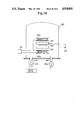
- FIG. 14 is a schematic view illustrating an example of an apparatus for carrying out the process of the first process of this invention.
- FIG. 15 is a plan view of the sheet-like electrode used therein;
- FIG. 16 is a view explanatory of a substrate on which a diamond-like substance is formed for measuring electrical resistance of the diamond-like substance in Example 1-(2);
- FIG. 17, FIG. 18 and FIG. 19 are schematic views of other examples of the apparatus for carrying out the process of this invention.
- the organic compound may include, for example, chain or cyclic saturated hydrocarbons such as methane, ethane, propane, butane, pentane, octane and cyclohexane; unsaturated hydrocarbons containing a double bond or triple bond, such as ethylene, propylene, butadiene, benzene, styrene, acetylene and allene; halogenated alkanes such as monofluoromethane, difluoromethane, trifluoromethane, tetrafluoromethane, monochloromethane, dichloromethane, trichloromethane, tetrachloromethane, monofluorodichloromethane, monofluoroethane, trifluoroethane, tetrafluoroethane, pentafluoroethane,
- chain or cyclic saturated hydrocarbons such as methane, ethane, propane, butane, pen
- perfluoropropane dichloropropane, tetrachloropropane, hexachloropropane, perchloropropane, difluorodichlropropane, tetrafluorodichloropropane, bromomethane, methylene bromide, bromoform, carbon tetrabromide, tetrabromoethane, pentabromoethane, methyl iodide, diiodomethane, monofluorobutane, trifluorobutane, tetrafluorobutane, octafluorobutane, difluorobutane, monofluoropentane, pentafluoropentane, octachloropentane, perchloropentane, trifluorotrichloropentane, tetrafluorohexane, nonachlorohexane, pentafluorotrichlor
- the inorganic compounds usable in the first process and second process of this invention may include carbon monoxide, carbon dioxide and diazomethane.
- gases of these organic compounds and inorganic compounds may also be mixed with rare gases such as helium, argon and xenon or gases such as hydrogen, oxygen and nitrogen. These gases may be used alone or in combination of two or more.
- carbon-containing organic compounds among the above, but preferred are carbon-containing organic compounds having 1 to 4 carbon atoms, such as methane, ethane, propane, butane, ethylene, propylene, butadiene, allylamine, methylamine, ethylamine, carbon disulfide, methanol, ethanol, formaldehyde and acetaldehyde, methyl ethyl ketone, formic acid, ethyl acetate, etc.
- carbon-containing organic compounds having 1 to 4 carbon atoms such as methane, ethane, propane, butane, ethylene, propylene, butadiene, allylamine, methylamine, ethylamine, carbon disulfide, methanol, ethanol, formaldehyde and acetaldehyde, methyl ethyl ketone, formic acid, ethyl acetate, etc.
- hydrogen and carbon-containing organic compounds may preferably be used in the proportion of from 0.1 to 5 mol, more preferably from 0.2 to 2 mol, of carbon-containing organic compounds per 100 mol of hydrogen.
- an overly small proportion of the carbon-containing organic compound tends to make slow the growth rate of the diamond like substance, and an overly large proportion of the same tends to result in formation of a diamond-like substance containing amorphous carbon in a large quantity.
- the high temperature or quasi-high temperature plasma is used.
- the high temperature plasma is known to refer to a plasma of Te/Tg ⁇ 1, assuming the electron temperature of plasma as Te and the gas temperature as Tg.
- the quasi-high temperature plasma is known to refer to a plasma of 1 ⁇ Te/Tg ⁇ 10.
- the discharge electrode used as the discharge electrode is a sheet-like electrode provided with a slit having a linear portion and connected to a microwave electric source (hereinafter referred to merely as "sheet-like electrode").
- the slit provided in the sheet like electrode may have a turned shape, or may be partly turned drawing an arc, but has at least one substantially linear portion satisfying the condition expressed by the equation:
- n is an integer of 1 or more, preferably 1 to 8, and more preferably 1 to 4 (hereinafter called "effective linear portion"). Absence of the effective linear portion in the slit may result in no normal microwave discharge, making it impossible to excite plasma in a desired state.
- This slit may further preferably be provided in such a manner that the whole length of the effective linear portions may be 0.1 to 6 cm/cm 2 with respect to the area of the substrate surface on which a film is intended to be formed or the area of the sheet-like electrode.
- the slit usually have a width of generally not less than 1 mm and less than ⁇ /2.
- FIG. 1 is a perspective view illustrating an example of the sheet-like electrode, in which a sheet-like electrode has a slit formed by making a out from an outer edge into the inside.
- This sheet-like electrode 1 comprises a conductive material, and is constituted of a flat sheet which is rectangular as a whole.
- a slit 3 is cut from a start point (cutting-in part) 2 nearest to its one end in parallel to a shorter side 4. and the slit 3 turns plural times at a right angle until it reaches an end point at a point 5 inside the sheet-like electrode.
- the slit 3 is constituted of six relatively long effective linear portions A 1 parallel to the shorter side 1 and six relatively short linear portions which are not effective linear portions (hereinafter called "non-effective linear portion(s)") B 1 parallel to the longer side, and is a single slit continuous from the start point 2 to the end point 5.
- non-effective linear portion(s) which are not effective linear portions
- FIG. 2 is a perspective view illustrating another example of the sheet-like electrode, which is a sheet-like electrode having the slit in plurality.
- This sheet-like electrode 21 also comprises a conductive material, and is constituted of a flat sheet which is rectangular as a whole.
- the slit 23 of the sheet-like electrode 21 comprises slits that form effective linear portions A 2 in parallel to shorter sides 24a and 24b of the sheet-like electrode 21, and the respective slits are separated.
- This sheet-like electrode 21 also has coaxial tube connecting portions 22a and 22b on its shorter sides 24a and 24b, which portions are respectively connected to coaxial tubes 28a and 28b.
- a slit 32 is provided in a sheet-like electrode 31 in such a fashion that a plurality of effective linear portions A 3 only are continuously connected with each other through angles ⁇ .
- a slit 42 is provided in a sheet-like electrode 41 in such a fashion that sets of two effective linear portions A 4 connected with each other through angles ⁇ are repeated in some number with the interposition of shorter non-effective linear portion B 4 .
- FIG. 3 a slit 32 is provided in a sheet-like electrode 31 in such a fashion that a plurality of effective linear portions A 3 only are continuously connected with each other through angles ⁇ .
- a slit cut in from the middle 52 of a longer side 51 is branched at the position of a point 54, and thereafter turns like that in FIG. 1 to form a plurality of effective linear portions A 5 before they respectively stop at end points 55 and 56.
- a plurality of slits 61, 62, 63, etc. each constituting the effective linear portion are provided in parallel to each other and at an angle ⁇ with respect to a longer side 65 of a sheet-like electrode 64.
- the sheet-like electrode having the shapes as illustrated in FIG. 7 and FIG. 8.
- a sheet-like electrode 70 is formed of two supporting rods 71a and 71b comprising a conductive material, and rods 72, 73, 74, 75, 76 and 77 comprising a conductive material provided across the supporting rods 71a and 71b in equal intervals in the form of a ladder.
- Small, rectangular spaces 78, 79, etc. surrounded by the rods correspond to the slit described above, and the length A 7 of the rectangular space in the longitudinal direction constitutes the effective linear portion.
- a plurality of blades comprising a conductive material are arranged in the same plane on the part at which only an inner guide tube 81 of a coaxial tube is bared, in such a fashion that the length 1 defined between both ends of blades opposing through the inner guide tube may correspond to the length of the effective linear portion.
- the shape of the sheet-like electrode there is no limitation on the shape of the sheet-like electrode, and its outline may be of any shape including a rectangular shape, as well as a circular shape.
- the sheet-like electrode may not particularly be required to be flat, and may have a curved surface as a whole or in part or may have convexes or concaves, corresponding to the three-dimensional shape of the substrate surface to be treated.
- FIG. 9 is a cross section illustrating a sheet-like electrode 93 suited to form a film on a spherical surface 92 of a substrate 91, where said electrode 93 is made to have an undersurface 94 formed in a concave surface in agreement with the spherical surface 92 of the substrate 91.
- FIG. 10 also is a cross section illustrating a sheet-like electrode 104 suited to form a film on a surface 103 of a substrate 102 having a rectangular convex 101, where said electrode 104 is formed with a rectangular concave in agreement with the convex 101 of the substrate 102, and is so designed that a film can be evenly formed on the whole top surface 103 of the substrate 102 as a whole.
- FIG. 10 also is a cross section illustrating a sheet-like electrode 104 suited to form a film on a surface 103 of a substrate 102 having a rectangular convex 101, where said electrode 104 is formed with a rectangular concave in agreement
- FIG. 11 is a cross section illustrating a sheet-like electrode 114 suited to form a film simultaneously on the surfaces 112 and 113 of a sheet-like substrate, where said electrode 114 is turned in U-shape and so designed that films can be formed on the whole of both surfaces 112 and 113 of the substrate 111.
- the sheet-like electrode may also be provided in plurality and in parallel with appropriate spacing, thereby making it possible to form films simultaneously on both surfaces of the substrate.
- Methods of introducing microwaves to the sheet-like electrode used in the first process may include, for example, a method in which an end of a coaxial cable or coaxial tube connected at the other end to a waveguide is connected to the sheet-like electrode, a method in which an end of a coaxial cable or coaxial tube connected at the other end to a waveguide is connected to one end of a parallel wire line and thereafter the other end of the parallel wire line is connected to the electrode, and a method in which an antenna provided in a waveguide and an antenna provided for the electrode are used.
- Methods of introducing microwaves to the sheet-like electrode may also include a method in which a microwave is introduced to one end of the sheet-like electrode and, at the same time, another microwave is also introduced to the other end thereof, and a method in which a microwave is introduced to one end of the sheet-like electrode and a coaxial tube or waveguide is connected to the other end thereof, which is then connected to a termination (i.e., dummy load).
- a termination i.e., dummy load
- Such methods of introducing the microwave to the sheet-like electrode may include (a) a method in which slits are arranged in the sheet-like electrode in a point-symmetrical or line-symmetrical fashion, and microwaves are introduced to symmetrically related two points on the electrode from respectively independent electric sources, and (b) a method in which slits are arranged in the sheet-like electrode in a point-symmetrical or line-symmetrical fashion, and microwaves are introduced to one of symmetrically related two points on the electrode, to the other of which a coaxial tube or waveguide is connected, which is then connected to a termination.
- the termination is a device to let microwaves having not been consumed in generating plasma escape in a liquid such as water or oil through a waveguide or coaxial tube.
- the magnetic flux density in the vicinity of the sheet like electrode may preferably be maintained at from 500 to 2,000 gauss, and an electromagnet, for example, can be used as a means for applying the magnetic field.
- a plasma zone in the form of mat (hereinafter called mat-like plasma zone) is so formed that it may cover the surface of the sheet-like electrode.
- the thickness represented by L in mm and the area represented by S in mm 2 of the mat-like plasma zone may preferably have a relation of:
- the plasma zone has an average energy density of 10 W/cm 3 or more.
- the value of S/L otherwise 200 or less may result in formation of a plasma zone having a small two dimensional breadth, making it impossible to make large so much the area on which a film can be formed.
- the plasma zone may preferably have a thickness of usually from 1 to 40 mm, preferably from 3 to 20 mm.
- the plasma zone may also preferably have an energy density of 10 W/cm 3 or more on average, preferably from 10 to 1,000 W/cm 3 .
- the energy density otherwise less than 10 W/cm 3 on average may result in a lowering of the rate of film formation on a large-area substrate surface.
- the material for the sheet-like electrode so long as it is a conductive material, and, specifically, there can be used any materials having a conductivity of 10 2 ohm -1 cm -1 or more at room temperature and usually having a good thermal resistance at 600° C. or more.
- Such materials may include, for example, transition metals such as iron, cobalt, nickel, manganese, chromium, vanadium, titanium, copper, zinc, yttrium, ruthenium, zirconium, niobium, molybdenum, rhodium, palladium, silver, tantaium, tungsten, rhenium, platinum, gold, thallium, lead and bismuth; aluminum; alloys of the above transition metals or aluminum, such as stainless steel, brass, bronze and super alloy; dispersion reinforce alloys comprising metal oxides dispersed in a metal, such as copper-alumina, copper-silicon oxide, silver-alumina, silver-cadmium oxide and nickel yttrium oxide; carbon materials such as carbon and graphite; and preferred among these are materials having a conductivity of 10 5 ohm -1 cm -1 or more, including copper, silver, aluminum, copper alloys and copper-alumina dispersion reinforced alloys.
- transition metals such as iron, cobal
- the sheet-like electrode is fixed in a reaction vessel to be used, with an electrical insulator.
- the electrical insulator that can be used may include, for example, inorganic materials such as alumina, boron nitride, quartz glass, silicon nitride and zirconium oxide; and organic polymers such as nylon and polyethylene.
- inorganic materials must be used in the case of a high temperature.
- a gas containing at least one selected from the group consisting of an organic compound and an inorganic compound is positioned in the reaction vessel.
- Flow rate of these gases may range generally from 0.1 to 100,000 cc(STP)/min per 100 lit. of inner volume of the reaction vessel.
- Average pressure in the reaction vessel may range usually from 0.5 to 760 Torr, preferably from 1 to 200 Torr. These are expressed as general ranges, and may be selected depending on the type of films to be formed.
- the carbon-containing organic compound and hydrogen are used, where the gas flow rate of the carbon-containing organic compound may range usually from 0.01 to 10,000 cc(STP)/min per 100 lit. of inner volume of the reaction vessel, and the flow rate of hydrogen may range from 0.1 to 10,000 cc(STP)/min per 100 lit. of inner volume of the reaction vessel.
- hydrogen and the carbon-containing organic compound may be separately fed to the reaction zone and then subjected to microwave discharge while mixing, or may be fed to the reaction zone in the form of a previously mixed gas and then subjected to the microwave discharge.
- a rare gas such as helium, argon or xenon may be mixed into the hydrogen, carbon-containing organic compound, or the mixed gas of these.
- the proportion of the rare gas may preferably be 80 mol or less per 100 mol of hydrogen.
- the mat-like plasma usually with a thickness of 1 to 20 mm in approximation is generated over the whole surface of the sheet-like electrode.
- a substrate may be so disposed previously or thereafter that the substrate surface to be treated may come into contact with the plasma thus excited, so that the desired film comprising the diamond-like substance can be formed on the substrate surface.
- the sheet like electrode has an area of 10,000 mm 2
- an applied electric power of about 1.5 kW results in excitation of plasma of about 5 mm in thickness on the surface of the electrode.
- Lowering of the applied electric power to 0.8 kW results in a plasma thickness lessened to about 2 mm, but the desired film comprising the diamond-like substance can be formed by bringing the substrate to come near to the electrode surface.
- the plasma of the gas containing at least one selected from the group consisting of an organic compound and inorganic compound is generated by DC discharge and force to move by applying a magnetic field.
- the plasma generated by DC discharge comprises a high temperature or quasi-high temperature plasma generated in the form of an arc (hereinafter simply called "arced plasma").
- Electrodes As illustrated in FIGS. 12A to 12C or FIG. 13.
- FIG. 12A illustrates discharge electrodes comprising a pair of rod-like electrodes 121 connected to a DC electric source, and the two electrodes 121 are fixed so as to give a space, for example, of from 1 to 10 mm by use of an insulator 122 comprising aluminum or the like.
- the arced plasma is generated at part between the discharge electrodes, and forced to move in the longitudinal direction of the rod-like electrodes, as shown by arrow X in the figure, by applying a magnetic field formed by a magnet (not shown).
- the arced plasma generated at part between the discharge electrodes comes to be in the state that it protrudes up and down the discharge electrodes, so that a film can be formed on a substrate set near to the discharge electrodes.
- FIG. 12B illustrates an example of the discharge electrodes comprised of three or more rod-like electrodes 121 similar to those shown in FIG. 12A, which is suited to form films having a larger area.
- FIG. 12C illustrates an example in which a disc-like electrode 123 and electrodes 124, 126 and 126 comprised of ring shaped flat sheets are concentrically arranged and circular slits 127 are respectively formed therebetween, where the respective electrodes 123 to 126 are connected to a DC electric source as shown in the figure.
- the arced plasma is generated at part of each circular slit 127 and moves along the circular slit 127 by the effect of the magnetic field formed by an electromagnet (not shown).
- each circular slit 127 comes to be in the state that it protrudes up and down the ring-shaped electrodes, and forced to move along the circular slit 127 by application of a magnetic field formed by an electromagnet, for instance, so that a film can be formed on a substrate set near to the discharge electrodes.
- a refrigerant may preferably be channeled inside the discharge electrodes to effect cooling.
- Materials for the discharge electrodes used in the second process may include the same conductive materials process.
- a voltage of from 10 to 900 volt is applied between the electrodes by using a DC electric source.
- a gas containing at least one selected from the group consisting of an organic compound and an inorganic compound is flowed in the reaction vessel, and flow rate of these gases usually ranges from 100 to 100,000 cc(STP)/min per 100 lit. of inner volume of the reaction vessel.
- the gas may preferably be positioned between the electrodes in the form of a jet flow so that the arced plasma is forced to jet from the discharge electrodes like a plasma jet.
- gas flow velocity between the electrodes, necessary for generating the arced plasma like a jet may preferably be set to from 0.01 to 600 m/sec, particularly preferably from 0.05 to 100 m/sec.
- Average pressure in the reaction vessel may range usually from 10 to 760 Torr, and energy density of the plasma may range usually from 10 to 1,000 W/cm 3 on time average.
- Methods by which the gas is fed to the reaction zone in the second process of this invention may include the same methods as in the first process.
- a pipe 131 as illustrated in FIG. 13 is set on the discharge electrodes 132 and a gas is fed through this pipe 131.
- This pipe 131 is provided with a gas-jetting slit 133 in the manner that the slit may face the discharge electrodes 132 and be positioned between two adjacent discharge electrodes, so that the gas can be fed from this gas-jetting slit to between the two adjacent discharge electrodes in the form of a jet flow.
- the generated arced plasma is forced to move by applying a magnetic field.
- This magnetic field is applied in the direction perpendicular to the direction of the flow of electric discharge current caused by DC discharge.
- Magnitude of magnetic flux density ranges usually from 80 to 2,000 gauss.
- an electromagnet for forming a magnetic field in the direction perpendicular to the direction of the flow of electric discharge current caused by DC discharge is placed, for example, at the upper and lower parts or right and left parts of the discharge electrodes as exemplified in the above.
- the position of the discharge between the discharge electrodes can be moved by applying this electric field, and, when, for example, the discharge electrodes as shown in FIG. 12A or FIG. 12C are used, a plasma sensor having the function to give a command to reverse the direction of the magnetic field at every time when it detects the plasma may be provided at both ends of a section in which the arced plasma reciprocates, thus enabling the reversal of the direction of movement.
- This reversal of the direction of the magnetic field may also be achieved by previously measuring the velocity of movement of the arced plasma, and automatically reversing the direction of the electric current for the electromagnet according to a period, for example, of about 1 second or less, determined on the basis of the measurements.
- the first and second processes of this invention is carried out in a reaction vessel, but there is no particular limitation on the type of the reaction vessel to be used, and may be included bell jar reaction vessels, as well as those exemplified by rectangular parallelepiped reaction vessels. There is also no particular limitation on a vacuum exhaust system connected to the reaction vessel, and there can be used those of various types commonly used.
- the first and second processes of this invention may also optionally provided with, for example, a substrate-supporting means such as a substrate stand, a substrate-heating means and a substrate cooling means.
- a substrate-supporting means such as a substrate stand, a substrate-heating means and a substrate cooling means.
- the substrate temperature may preferably be maintained at 600° to 900° C.
- an infrared image furnace or a resistance heater can be used as the substrate stand, and, when it is necessary to cool the substrate, a water-cooling type cooling stand can be used as the substrate stand.
- ceramics such as alumina, tungsten carbide and titanium nitride: semiconductors such as silicon, germanium and gallium arsenic; metals such as molybdenum, tungsten, tantalum. copper and iron; dispersion reinforced alloys comprising metal oxide particles dispersed in copper or copper alloys; and quartz glass.
- These substrates may be used as they are, or may be used after surfaces are scratched using a diamond paste or the like to make it easier to form films.
- This apparatus is equipped with a sheet-like electrode 142 fixed horizontally in a bell jar reaction vessel 141, and the electrode 142 is connected to a microwave electric source for introducing a microwave with a wavelength of 122 mm through a coaxial cable 143 and a microwave-introducing terminal 144.
- a substrate stand 145 made of alumina, provided in the reaction vessel is equipped with an infrared image furnace, which can heat to a desired temperature a substrate 146 placed on the substrate stand.
- an exhaust tube 147 connected to a vacuum exhaust system, and a gas inlet tube for introducing a gas used for generating plasma to which valves 147 and 148 are respectively provided.
- the sheet-like electrode 142 is made of copper and comprised of two sheets of the sheet like electrode exemplified in FIG. 5, which are arranged and connected to the coaxial cable 143 as illustrated in FIG. 15 and are rectangular sheet-like electrodes having a dimension of 160 ⁇ 180 ⁇ 1 mm when the two sheets are put side by side.
- a slit 151 has a slit width of 4 mm, twenty-two (22) effective linear portions whose length X shown in FIG. 15 is 61 mm, and non-effective linear portions which keep every two adjacent effective linear portions apart by a distance of 15 mm as shown by Y in FIG. 15.
- Used as the substrate 146 was a silicon wafer having a diameter of 2 inches. This substrate was placed in a beaker together with diamond particles having an average particle diameter of 3 micrometers, maintained for 10 minutes in an ultrasonic washer filled with water together with the whole beaker to carry out a pretreatment to make scratches on the substrate surface, and thereafter placed on the substrate stand. The top surface of the substrate and the sheet-like electrode was held 4 mm apart.
- Test Nos. 1 to 14 kind of gas used for generating plasma, pressure, energy density of plasma and substrate temperature were varied as shown in Table 1, and treatments of the tests were carried out for 2 hours under the conditions respectively shown in Table 1.
- the energy density is expressed by a value obtained by dividing the applied microwave electric power by the volume of generated plasma.
- the substrate temperature was measured by using an alumel-chromel thermocouple fixed to the substrate, making control by adjusting the electric power for the infrared image furnace. At the time of the measurement, however, the application of the microwave electric power was stopped for a short time.
- This apparatus has the same constitution as the apparatus illustrated in FIG. 14 except that the apparatus illustrated in FIG. 14 is additionally provided with a coil 171a above the sheet-like electrode 172 and also a coil 171b beneath the substrate stand 145, and further a sheet-like electrode 172 made of molybdenum having the same shape and dimension was used in place of the sheet-like electrode 142 made of copper.
- Used as the substrate 146 was the same as in Example 1, and the top surface of the substrate 146 and the sheet-like electrode 172 were held 4 mm apart.
- the magnetic field produced by the coils 171a and 171b were set so as to give 875 gauss in the vicinity of the substrate 146.
- Formation of films comprising a diamond-like substance was carried out on substrates, using the same apparatus as the apparatus schematically illustrated in FIG. 17 and used in Example 2, except that the sheet-like electrode 172 used therein was replaced by a sheet-like electrode having the slits as exemplified in FIG. 2, having a rectangular shape of 100 ⁇ 80 ⁇ 1 mm and made of molybdenum, in which five silts having a length of 61 mm at the effective linear portion A 2 and a slit width B 2 of 12 mm are provided at intervals of 7 mm.
- This apparatus is equipped with discharge electrodes 182 internally holding a cooling refrigerant pipe (not shown) and fixed horizontally in a bell ar reaction vessel 181, and said electrodes 182 are connected to a DC electric source 186.
- a substrate stand 183 made of alumina and provided inside the reaction vessel is equipped therein with an infrared image furnace and a cooling refrigerant pipe (not shown), so that a substrate 184 placed on said substrate stand can be maintained at a desired temperature.
- Electromagnets 185a and 185b are further provided above the discharge electrodes 12 and beneath the substrate stand 184, respectively, in such a manner that the electromagnets may sandwich these.
- the electromagnets 185a and connected to an electric source 187 provided outside the reaction vessel, and can form electric field in the direction perpendicular to the electric current flowing between the electrodes.
- an exhaust tube Provided at the bottom of the reaction vessel are an exhaust tube, a gas inlet tube and so forth in the same manner as in the apparatus illustrated in FIG. 14. These are denoted in FIG. 18 with the same numerals as in FIG. 14.
- the discharge electrodes 182 correspond to the electrodes of the type shown in FIG. 12B, and are comprised of five rod-like electrodes with a dimension of 10 ⁇ 10 ⁇ 200 mm each, which are so arranged that anodes and cathodes may alternate.
- the electrodes serving as anodes are made of copper
- the electrodes serving as cathodes are made of tungsten. Electrodes adjacent to each other have a spacing of 5 mm, and both ends of each discharge electrode are fixed with insulators 122 made of alumina.
- a silicon wafer of 70 ⁇ 200 ⁇ 0.3 mm was placed on the substrate stand 183.
- the top surface of the substrate and the discharge electrodes were held 5 mm apart. Voltage of the electric source 187 was adjusted so that electric field produced by the electromagnets 185a and 185b may come to be about 400 gauss in the vicinity of the discharge electrodes 182, thus forcing the arced plasma to move. Plasma sensors (not shown) were further provided on both ends of the discharge electrodes 182 to reverse the electric current of the electric source 187 at every time when the arced plasma reaches extremities of the discharge electrodes 182.
- FIG. 19 Using the apparatus schematically illustrated in FIG. 19, formation of films comprising a diamond-like substance was carried out on substrates.
- the same components as in FIG. i3 and FIG. 18 are denoted by the same numerals.
- This apparatus is the same as the apparatus illustrated in FIG. 18 and used in Example 4, except that four pipes 133 having a gas-jetting slit 133 from which a plasma generating was is flowed into between the discharge electrodes in the form of a jet flow, as exemplified in FIG. 13, was set between the discharge electrodes 182 and the electromagnet 185a positioned above the discharge electrodes 182.
- This gas jetting slit 133 is 1 mm wide and 200 mm long, and provided in the manner that it may face the center of the slit between electrodes as described with reference to FIG. 13.
- the gas jetting slit 133 and the discharge electrodes 182 are held 5 mm apart.
- the pipe 131 is connected to a gas inlet tube 192 for introducing plasma generating gas, provided at the bottom of a reaction vessel 191.
- An exhaust tube 193 is also connected to the bottom of the reaction vessel 191.
- Test Nos. 35 to 42 kind of gas used for generating plasma, pressure, energy density of plasma and substrate temperature were varied as shown in Table 5, and treatments of these tests were carried out for 1 hour under the conditions respectively shown in Table 5.
Abstract
Description
1=n×λ/2
S/L>200
                                  TABLE 1
__________________________________________________________________________
                                  Aver-
                                      Film
                      Sub- Plasma age thick-
                 Plasma
                      strate
                           zone   film
                                      ness
   Kind of gas   energy
                      temper-
                           thick- thick-
                                      scat-
Test
   & gas flow rate
            Pressure
                 density
                      ature
                           ness   ness
                                      tering
                                          Crystal-
No.
   cc(STP)/min
            (Torr)
                 (W/cm.sup.3)
                      (°C.)
                           (mm)
                               S/L
                                  (μm)
                                      (μm)
                                          linity
__________________________________________________________________________
1  CH.sub.4 (10) +
            20   16   800  12  2,400
                                  4   <1  >10
   H.sub.2 (1,000)
2  CH.sub.4 (10) +
            100  24   780  4   7,200
                                  6   <1  >10
   H.sub.2 (1,000)
3  CH.sub.3 OH(15) +
            10   12   750  14  2,057
                                  5   <1  >10
   H.sub.2 (1,000)
4  CH.sub.3 OH(15) +
            80   19   850  6   4,800
                                  12  4   >10
   H.sub.2 (1,000)
5  CH.sub.3 NH.sub.2 (10) +
            5    13   810  14  2,057
                                  5   <1  >10
   H.sub.2 (800)
6  CH.sub.3 NH.sub.2 (10) +
            100  27   740  4   7,200
                                  7   <1  >10
   H.sub.2 (800)
7  CS.sub.2 (8) + H.sub.2 (700)
            10   14   820  16  1,800
                                  8   <1  5
8  CS.sub.2 (8) + H.sub.2 (700)
            90   22   840  4   7,200
                                  9   2   7
9  CO.sub.2 (10) +
            40   21   830  10  2,880
                                  1   <1  6
   H.sub.2 (1,200)
10 CO.sub.2 (10) +
            80   35   910  6   4,800
                                  2   <1  7
   H.sub.2 (1,200)
11 CH.sub.3 F(10) +
            20   16   820  12  2,400
                                  7   <1  >10
   H.sub.2 (1,000)
12 CH.sub.3 F(10) +
            100  24   840  4   7,200
                                  9   2   >10
   H.sub.2 (1,000)
13 CF.sub.4 (10) +
            15   20   830  12  2,400
                                  8   >1  8
   H.sub.2 (1,000)
14 CF.sub.4 (10) +
            40   27   870  10  2,880
                                  10  3   7
   H.sub.2 (1,000)
__________________________________________________________________________
              TABLE 2
______________________________________
(Unit: ohm)
Measure
point    Test 15       Test 16  Test 17
______________________________________
1        5 × 10.sup.11
                       5 × 10.sup.11
                                7 × 10.sup.11
2        6 × 10.sup.11
                       7 × 10.sup.11
                                8 × 10.sup.11
3        6 × 10.sup.11
                       8 × 10.sup.11
                                8 × 10.sup.11
4        6 × 10.sup.11
                       8 × 10.sup.11
                                8 × 10.sup.11
5        6 × 10.sup.11
                       7 × 10.sup.11
                                7 × 10.sup.11
6        4 × 10.sup.11
                       6 × 10.sup.11
                                7 × 10.sup.11
7        4 × 10.sup.11
                       7 × 10.sup.11
                                8 × 10.sup.11
8        6 × 10.sup.11
                       8 × 10.sup.11
                                7 × 10.sup.11
9        6 × 10.sup.11
                       9 × 10.sup.11
                                8 × 10.sup.11
10       6 × 10.sup.11
                       9 × 10.sup.11
                                8 × 10.sup.11
11       6 × 10.sup.11
                       8 × 10.sup.11
                                8 ×  10.sup.11
12       4 × 10.sup.11
                       6 × 10.sup.11
                                7 × 10.sup.11
13       5 × 10.sup.11
                       5 × 10.sup.11
                                8 × 10.sup.11
14       5 × 10.sup.11
                       7 × 10.sup.11
                                8 × 10.sup.11
15       6 × 10.sup.11
                       8 × 10.sup.11
                                7 × 10.sup.11
16       6 × 10.sup.11
                       8 × 10.sup.11
                                7 × 10.sup.11
17       6 × 10.sup.11
                       7 × 10.sup.11
                                8 × 10.sup.11
18       5 × 10.sup.11
                       7 × 10.sup.11
                                7 × 10.sup.11
______________________________________
                                  TABLE 3
__________________________________________________________________________
                                 Aver-
                                     Film
                     Sub- Plasma age thick-
                Plasma
                     strate
                          zone   film
                                     ness
   Kind of gas  energy
                     temper-
                          thick- thick-
                                     scat-
Test
   & gas flow rate
           Pressure
                density
                     ature
                          ness   ness
                                     tering
                                         Crystal-
No.
   cc(STP)/min
           (Torr)
                (W/cm.sup.3)
                     (°C.)
                          (mm)
                              S/L
                                 (μm)
                                     (μm)
                                         linity
__________________________________________________________________________
19 CH.sub.4 (10) +
           20   30   820  18  3,600
                                 5   <2  >10
   H.sub.2 (1,000)
20 CH.sub.4 (10) +
           100  42   810  10  2,880
                                 7   <2  >10
   H.sub.2 (1,000)
21 CH.sub.3 OH(15) +
           10   28   820  20  1,440
                                 6   <2  >10
   H.sub.2 (1,000)
22 CH.sub.3 OH(15) +
           80   38   810  12  2,400
                                 14  <5  >10
   H.sub.2 (1,000)
23 CH.sub.4 (10) +
           20   29   820  18  444
                                 5   <1  >10
   H.sub.2 (1,000)
24 CH.sub.4 (10) +
           100  43   815  10  800
                                 8   <2  >10
   H.sub.2 (1,000)
25 CH.sub.3 OH(15) +
           10   28   815  20  400
                                 6   <2  5
   H.sub.2 (1,000)
26 CH.sub.3 OH(15) +
           80   39   810  12  667
                                 15  <5  7
   H.sub.2 (1,000)
__________________________________________________________________________
                                  TABLE 4
__________________________________________________________________________
                           Aver-
                               Film
                      Sub- age thick-
                 Plasma
                      strate
                           film
                               ness
   Kind of gas
            Average
                 energy
                      temper-
                           thick-
                               scat-
Test
   & gas flow rate
            pressure
                 density
                      ature
                           ness
                               tering
                                   Crystal-
No.
   cc(STP)/min
            (Torr)
                 (W/cm.sup.3)
                      (°C.)
                           (μm)
                               (μm)
                                   linity
__________________________________________________________________________
27 CH.sub.4 (10) +
            20   90   800  22  3   >10
   H.sub.2 (1,000)
28 CH.sub.4 (10) +
            100  200  600  14  2   8
   H.sub.2 (1,000)
29 CH.sub.3 OH(15) +
            10   80   550  12  2   6
   H.sub.2 (1,000)
30 CH.sub.3 OH(15) +
            80   170  750 18
                           3   8
   H.sub.2 (1,000)
31 CH.sub.3 NH.sub.2 (10) +
            5    50   850  16  2   >10
   H.sub.2 (800)
32 CH.sub.3 NH.sub.2 (10) +
            100  170  700  20  3   7
   H.sub.2 (800)
33 CO.sub.2 + H.sub.2 (1,200)
            40   100  800  14  2   >10
34 CO.sub.2 + H.sub. 2 (1,200)
            80   180  650  7   <1  7
__________________________________________________________________________
                                  TABLE 5
__________________________________________________________________________
                   Gas flow        Aver-
                                       Film
                   velocity   Sub- age thich-
                   between
                         Plasma
                              strate
                                   film
                                       ness
   Kind of gas
              Average
                   discharge
                         energy
                              temper-
                                   thick-
                                       scat-
Test
   & gas flow rate
              pressure
                   electrodes
                         density
                              ature
                                   ness
                                       tering
                                           Crystal-
No.
   cc(STP)/min
              (Torr)
                   (m/sec)
                         (W/cm.sup.3)
                              (°C.)
                                   (μm)
                                       (μm)
                                           linity
__________________________________________________________________________
35 CH.sub.4 (10) +
              20   3.2   120  850  60  5   >10
   H.sub.2 (1,000)
36 CH.sub.4 (10) +
              100  0.6   300  620  42  4   7
   H.sub.2 (1,000)
37 CH.sub.3 OH(15) +
              10   6.4   100  600  55  3   7
   H.sub.2 (1,000)
38 CH.sub.3 OH(15)
              80   1.1   200  800  67 4
                                       >10
   H.sub.2 (1,000)
39 CH.sub.3 NH.sub.2 (10) +
              5    10.3  80   900  47  2   >10
   H.sub.2 (800)
40 CH.sub.3 NH.sub.2 (10) +
              100  1.2   250  780  60  4   8
   H.sub.2 (800)
41 CO.sub.2 (10) + H.sub.2 (1,200)
              40   1.9   150  870  47  3   >10
42 CO.sub.2 (10) + H.sub.2 (1,200)
              80   0.95  330  710  33  <1  9
__________________________________________________________________________
Claims (22)
S/L>200,
l=n×λ/2
Applications Claiming Priority (4)
| Application Number | Priority Date | Filing Date | Title |
|---|---|---|---|
| JP22791087 | 1987-09-11 | ||
| JP62-227910 | 1987-09-11 | ||
| JP62-267768 | 1987-10-23 | ||
| JP62267768A JPH01109699A (en) | 1987-10-23 | 1987-10-23 | Plasma processing device |
Publications (1)
| Publication Number | Publication Date |
|---|---|
| US4910041A true US4910041A (en) | 1990-03-20 |
Family
ID=26527945
Family Applications (1)
| Application Number | Title | Priority Date | Filing Date |
|---|---|---|---|
| US07/242,263 Expired - Lifetime US4910041A (en) | 1987-09-11 | 1988-09-09 | Film formation process |
Country Status (2)
| Country | Link |
|---|---|
| US (1) | US4910041A (en) |
| DE (1) | DE3830430A1 (en) |
Cited By (21)
| Publication number | Priority date | Publication date | Assignee | Title |
|---|---|---|---|---|
| US5035828A (en) * | 1988-12-20 | 1991-07-30 | Daikin Industries, Ltd. | Solvents containing dichlorotetrafluoropropane |
| US5055421A (en) * | 1987-08-03 | 1991-10-08 | Siemens Aktiengesellschaft | Method for the plasma deposition of hydrogenated, amorphous carbon using predetermined retention times of gaseous hydrocarbons |
| US5071670A (en) * | 1990-06-11 | 1991-12-10 | Kelly Michael A | Method for chemical vapor deposition under a single reactor vessel divided into separate reaction chambers each with its own depositing and exhausting means |
| GB2244721A (en) * | 1990-05-03 | 1991-12-11 | Northern Telecom Ltd | Plasma processing apparatus |
| US5194170A (en) * | 1992-04-02 | 1993-03-16 | E. I. Du Pont De Nemours And Company | Binary azeotropic compositions of 1,1,2,2,3,3,4,4-octafluorobutane and either tran-1,2-dichloroethylene, cis 1,2-dichloroethylene, or 1-1 dichloroethane |
| US5219490A (en) * | 1992-04-27 | 1993-06-15 | Allied-Signal Inc. | Azeotrope-like compositions of 1,1,2,3,3-pentafluoropropane |
| US5250208A (en) * | 1992-04-02 | 1993-10-05 | E. I. Du Pont De Nemours And Company | Ternary azeotropic compositions |
| US5522932A (en) * | 1993-05-14 | 1996-06-04 | Applied Materials, Inc. | Corrosion-resistant apparatus |
| US5525392A (en) * | 1992-12-10 | 1996-06-11 | International Business Machines Corporation | Magnetic recording medium having a fluorinated polymeric protective layer formed by an ion beam |
| US5554415A (en) * | 1994-01-18 | 1996-09-10 | Qqc, Inc. | Substrate coating techniques, including fabricating materials on a surface of a substrate |
| EP0737256A1 (en) * | 1993-06-04 | 1996-10-16 | Applied Science And Technology | Microwave plasma reactor |
| US5620754A (en) * | 1994-01-21 | 1997-04-15 | Qqc, Inc. | Method of treating and coating substrates |
| US5626922A (en) * | 1990-09-25 | 1997-05-06 | Semiconductor Energy Laboratory Co., Ltd. | Plasma processing method |
| US5731046A (en) * | 1994-01-18 | 1998-03-24 | Qqc, Inc. | Fabrication of diamond and diamond-like carbon coatings |
| US5869147A (en) * | 1994-05-20 | 1999-02-09 | Widia Gmbh | Method of making a multilayer tool surface with PCNA interruption of CVD, and tool made by the process |
| US5891253A (en) * | 1993-05-14 | 1999-04-06 | Applied Materials, Inc. | Corrosion resistant apparatus |
| US6001431A (en) * | 1992-12-28 | 1999-12-14 | Semiconductor Energy Laboratory Co., Ltd. | Process for fabricating a magnetic recording medium |
| US6001432A (en) * | 1992-11-19 | 1999-12-14 | Semiconductor Energy Laboratory Co., Ltd. | Apparatus for forming films on a substrate |
| US6461529B1 (en) * | 1999-04-26 | 2002-10-08 | International Business Machines Corporation | Anisotropic nitride etch process with high selectivity to oxide and photoresist layers in a damascene etch scheme |
| US7264850B1 (en) | 1992-12-28 | 2007-09-04 | Semiconductor Energy Laboratory Co., Ltd. | Process for treating a substrate with a plasma |
| US20090199655A1 (en) * | 2005-07-05 | 2009-08-13 | Endress + Hauser Flowtec Ag | Method for Determining Working Point of a Magneto-Inductive Flow Measuring Device |
Families Citing this family (4)
| Publication number | Priority date | Publication date | Assignee | Title |
|---|---|---|---|---|
| JP2785442B2 (en) * | 1990-05-15 | 1998-08-13 | 三菱重工業株式会社 | Plasma CVD equipment |
| DE4118072C2 (en) * | 1991-06-01 | 1997-08-07 | Linde Ag | Process for shock wave coating of substrates |
| DE19955671B4 (en) * | 1999-11-19 | 2004-07-22 | Muegge Electronic Gmbh | Device for generating plasma |
| DE102007020419A1 (en) | 2007-04-27 | 2008-11-06 | Forschungsverbund Berlin E.V. | Electrode for plasma generator |
Citations (1)
| Publication number | Priority date | Publication date | Assignee | Title |
|---|---|---|---|---|
| US4816113A (en) * | 1987-02-24 | 1989-03-28 | Semiconductor Energy Laboratory Co., Ltd. | Method of eliminating undesirable carbon product deposited on the inside of a reaction chamber |
-
1988
- 1988-09-07 DE DE3830430A patent/DE3830430A1/en not_active Withdrawn
- 1988-09-09 US US07/242,263 patent/US4910041A/en not_active Expired - Lifetime
Patent Citations (1)
| Publication number | Priority date | Publication date | Assignee | Title |
|---|---|---|---|---|
| US4816113A (en) * | 1987-02-24 | 1989-03-28 | Semiconductor Energy Laboratory Co., Ltd. | Method of eliminating undesirable carbon product deposited on the inside of a reaction chamber |
Cited By (30)
| Publication number | Priority date | Publication date | Assignee | Title |
|---|---|---|---|---|
| US5055421A (en) * | 1987-08-03 | 1991-10-08 | Siemens Aktiengesellschaft | Method for the plasma deposition of hydrogenated, amorphous carbon using predetermined retention times of gaseous hydrocarbons |
| US5035828A (en) * | 1988-12-20 | 1991-07-30 | Daikin Industries, Ltd. | Solvents containing dichlorotetrafluoropropane |
| GB2244721A (en) * | 1990-05-03 | 1991-12-11 | Northern Telecom Ltd | Plasma processing apparatus |
| GB2244721B (en) * | 1990-05-03 | 1993-05-19 | Northern Telecom Ltd | Plasma processing apparatus |
| US5071670A (en) * | 1990-06-11 | 1991-12-10 | Kelly Michael A | Method for chemical vapor deposition under a single reactor vessel divided into separate reaction chambers each with its own depositing and exhausting means |
| US5626922A (en) * | 1990-09-25 | 1997-05-06 | Semiconductor Energy Laboratory Co., Ltd. | Plasma processing method |
| US7125588B2 (en) | 1990-09-25 | 2006-10-24 | Semiconductor Energy Laboratory Co., Ltd. | Pulsed plasma CVD method for forming a film |
| US20040115365A1 (en) * | 1990-09-25 | 2004-06-17 | Semiconductor Energy Laboratory Co., Ltd. | Method for forming a film |
| US6660342B1 (en) | 1990-09-25 | 2003-12-09 | Semiconductor Energy Laboratory Co., Ltd. | Pulsed electromagnetic energy method for forming a film |
| US6110542A (en) * | 1990-09-25 | 2000-08-29 | Semiconductor Energy Laboratory Co., Ltd. | Method for forming a film |
| US5250208A (en) * | 1992-04-02 | 1993-10-05 | E. I. Du Pont De Nemours And Company | Ternary azeotropic compositions |
| US5194170A (en) * | 1992-04-02 | 1993-03-16 | E. I. Du Pont De Nemours And Company | Binary azeotropic compositions of 1,1,2,2,3,3,4,4-octafluorobutane and either tran-1,2-dichloroethylene, cis 1,2-dichloroethylene, or 1-1 dichloroethane |
| US5219490A (en) * | 1992-04-27 | 1993-06-15 | Allied-Signal Inc. | Azeotrope-like compositions of 1,1,2,3,3-pentafluoropropane |
| US6001432A (en) * | 1992-11-19 | 1999-12-14 | Semiconductor Energy Laboratory Co., Ltd. | Apparatus for forming films on a substrate |
| US5525392A (en) * | 1992-12-10 | 1996-06-11 | International Business Machines Corporation | Magnetic recording medium having a fluorinated polymeric protective layer formed by an ion beam |
| US7264850B1 (en) | 1992-12-28 | 2007-09-04 | Semiconductor Energy Laboratory Co., Ltd. | Process for treating a substrate with a plasma |
| US6001431A (en) * | 1992-12-28 | 1999-12-14 | Semiconductor Energy Laboratory Co., Ltd. | Process for fabricating a magnetic recording medium |
| US5522932A (en) * | 1993-05-14 | 1996-06-04 | Applied Materials, Inc. | Corrosion-resistant apparatus |
| US5593541A (en) * | 1993-05-14 | 1997-01-14 | Applied Materials, Inc. | Method of manufacturing using corrosion-resistant apparatus comprising rhodium |
| US5891253A (en) * | 1993-05-14 | 1999-04-06 | Applied Materials, Inc. | Corrosion resistant apparatus |
| EP0737256A4 (en) * | 1993-06-04 | 1996-12-27 | Applied Science Technology | Microwave plasma reactor |
| EP0737256A1 (en) * | 1993-06-04 | 1996-10-16 | Applied Science And Technology | Microwave plasma reactor |
| US5554415A (en) * | 1994-01-18 | 1996-09-10 | Qqc, Inc. | Substrate coating techniques, including fabricating materials on a surface of a substrate |
| US5731046A (en) * | 1994-01-18 | 1998-03-24 | Qqc, Inc. | Fabrication of diamond and diamond-like carbon coatings |
| US5620754A (en) * | 1994-01-21 | 1997-04-15 | Qqc, Inc. | Method of treating and coating substrates |
| US5869147A (en) * | 1994-05-20 | 1999-02-09 | Widia Gmbh | Method of making a multilayer tool surface with PCNA interruption of CVD, and tool made by the process |
| SG98375A1 (en) * | 1999-04-26 | 2003-09-19 | Ibm | Anisotropic nitride etch process with high selectivity to oxide and photoresist layers in a damascene etch scheme |
| US6461529B1 (en) * | 1999-04-26 | 2002-10-08 | International Business Machines Corporation | Anisotropic nitride etch process with high selectivity to oxide and photoresist layers in a damascene etch scheme |
| US20090199655A1 (en) * | 2005-07-05 | 2009-08-13 | Endress + Hauser Flowtec Ag | Method for Determining Working Point of a Magneto-Inductive Flow Measuring Device |
| US7661323B2 (en) * | 2005-07-05 | 2010-02-16 | Endress + Hauser Flowtec Ag | Method for determining working point of a magneto-inductive flow measuring device |
Also Published As
| Publication number | Publication date |
|---|---|
| DE3830430A1 (en) | 1989-03-23 |
Similar Documents
| Publication | Publication Date | Title |
|---|---|---|
| US4910041A (en) | Film formation process | |
| US4935303A (en) | Novel diamond-like carbon film and process for the production thereof | |
| US9909215B2 (en) | Method of CVD plasma processing with a toroidal plasma processing apparatus | |
| KR960015609B1 (en) | Plasma operation apparatus | |
| JP3411539B2 (en) | Plasma processing apparatus and plasma processing method | |
| Piscanec et al. | Raman spectroscopy of silicon nanowires | |
| EP1289003B1 (en) | Plasma processing apparatus | |
| JP5746147B2 (en) | Plasma generator, plasma generator array, and denaturing method using the array | |
| JP3697250B2 (en) | Plasma processing apparatus and method for producing carbon coating-formed plastic container | |
| WO1994026952A1 (en) | Apparatus and method for depositing diamond and refractory materials | |
| WO1990013909A1 (en) | Reactive ion etching apparatus | |
| JPS6223254B2 (en) | ||
| RU2136483C1 (en) | Abrasive material for precision treatment of surface and its manufacturing process | |
| US5164222A (en) | Cvd method for depositing a layer on an electrically conductive thin layer structure | |
| JPH01230496A (en) | Novel diamond carbon membrane and its production | |
| JPH01159379A (en) | Formation of film | |
| US6452400B1 (en) | Method of measuring negative ion density of plasma and plasma processing method and apparatus for carrying out the same | |
| JPH01109699A (en) | Plasma processing device | |
| JP2816365B2 (en) | Strain-free precision processing equipment by radical reaction | |
| JP3823001B2 (en) | Plasma processing equipment | |
| KR100256192B1 (en) | Plasma process apparatus and plasma process method | |
| KR20030077262A (en) | Apparatus For Plasma Chemical Vapor Deposition And Methode of Forming Thin Layer Utilizing The Same | |
| JP2597717B2 (en) | Discharge electrode of discharge treatment equipment | |
| JP4523566B2 (en) | Dry etching equipment | |
| JPH0627340B2 (en) | Hybrid plasma thin film synthesis method and device |
Legal Events
| Date | Code | Title | Description |
|---|---|---|---|
| FEPP | Fee payment procedure |
Free format text: PAYOR NUMBER ASSIGNED (ORIGINAL EVENT CODE: ASPN); ENTITY STATUS OF PATENT OWNER: LARGE ENTITY |
|
| AS | Assignment |
Owner name: JAPAN SYNTHETIC RUBBER CO., LTD., JAPAN Free format text: ASSIGNMENT OF ASSIGNORS INTEREST.;ASSIGNORS:YANAGIHARA, KENJI;KIMURA, MITUO;CHAWANYA, HITOSHI;AND OTHERS;REEL/FRAME:005211/0434 Effective date: 19880825 |
|
| STCF | Information on status: patent grant |
Free format text: PATENTED CASE |
|
| FEPP | Fee payment procedure |
Free format text: PAYOR NUMBER ASSIGNED (ORIGINAL EVENT CODE: ASPN); ENTITY STATUS OF PATENT OWNER: LARGE ENTITY Free format text: PAYER NUMBER DE-ASSIGNED (ORIGINAL EVENT CODE: RMPN); ENTITY STATUS OF PATENT OWNER: LARGE ENTITY |
|
| FPAY | Fee payment |
Year of fee payment: 4 |
|
| FPAY | Fee payment |
Year of fee payment: 8 |
|
| AS | Assignment |
Owner name: JSR CORPORATION, JAPAN Free format text: CHANGE OF NAME;ASSIGNOR:JAPAN SYNTHETIC RUBBER CO., LTD.;REEL/FRAME:010086/0530 Effective date: 19971210 |
|
| FPAY | Fee payment |
Year of fee payment: 12 |