US4912342A - Programmable logic device with array blocks with programmable clocking - Google Patents
Programmable logic device with array blocks with programmable clocking Download PDFInfo
- Publication number
- US4912342A US4912342A US07/407,411 US40741189A US4912342A US 4912342 A US4912342 A US 4912342A US 40741189 A US40741189 A US 40741189A US 4912342 A US4912342 A US 4912342A
- Authority
- US
- United States
- Prior art keywords
- terms
- term
- programmable
- signal
- logic
- Prior art date
- Legal status (The legal status is an assumption and is not a legal conclusion. Google has not performed a legal analysis and makes no representation as to the accuracy of the status listed.)
- Expired - Lifetime
Links
Images


Classifications
-
- H—ELECTRICITY
- H03—ELECTRONIC CIRCUITRY
- H03K—PULSE TECHNIQUE
- H03K19/00—Logic circuits, i.e. having at least two inputs acting on one output; Inverting circuits
- H03K19/02—Logic circuits, i.e. having at least two inputs acting on one output; Inverting circuits using specified components
- H03K19/173—Logic circuits, i.e. having at least two inputs acting on one output; Inverting circuits using specified components using elementary logic circuits as components
- H03K19/177—Logic circuits, i.e. having at least two inputs acting on one output; Inverting circuits using specified components using elementary logic circuits as components arranged in matrix form
- H03K19/17736—Structural details of routing resources
-
- H—ELECTRICITY
- H03—ELECTRONIC CIRCUITRY
- H03K—PULSE TECHNIQUE
- H03K19/00—Logic circuits, i.e. having at least two inputs acting on one output; Inverting circuits
- H03K19/02—Logic circuits, i.e. having at least two inputs acting on one output; Inverting circuits using specified components
- H03K19/173—Logic circuits, i.e. having at least two inputs acting on one output; Inverting circuits using specified components using elementary logic circuits as components
- H03K19/177—Logic circuits, i.e. having at least two inputs acting on one output; Inverting circuits using specified components using elementary logic circuits as components arranged in matrix form
- H03K19/17704—Logic circuits, i.e. having at least two inputs acting on one output; Inverting circuits using specified components using elementary logic circuits as components arranged in matrix form the logic functions being realised by the interconnection of rows and columns
-
- H—ELECTRICITY
- H03—ELECTRONIC CIRCUITRY
- H03K—PULSE TECHNIQUE
- H03K19/00—Logic circuits, i.e. having at least two inputs acting on one output; Inverting circuits
- H03K19/02—Logic circuits, i.e. having at least two inputs acting on one output; Inverting circuits using specified components
- H03K19/173—Logic circuits, i.e. having at least two inputs acting on one output; Inverting circuits using specified components using elementary logic circuits as components
- H03K19/177—Logic circuits, i.e. having at least two inputs acting on one output; Inverting circuits using specified components using elementary logic circuits as components arranged in matrix form
- H03K19/17736—Structural details of routing resources
- H03K19/1774—Structural details of routing resources for global signals, e.g. clock, reset
-
- H—ELECTRICITY
- H01—ELECTRIC ELEMENTS
- H01L—SEMICONDUCTOR DEVICES NOT COVERED BY CLASS H10
- H01L2224/00—Indexing scheme for arrangements for connecting or disconnecting semiconductor or solid-state bodies and methods related thereto as covered by H01L24/00
- H01L2224/01—Means for bonding being attached to, or being formed on, the surface to be connected, e.g. chip-to-package, die-attach, "first-level" interconnects; Manufacturing methods related thereto
- H01L2224/02—Bonding areas; Manufacturing methods related thereto
- H01L2224/04—Structure, shape, material or disposition of the bonding areas prior to the connecting process
- H01L2224/05—Structure, shape, material or disposition of the bonding areas prior to the connecting process of an individual bonding area
- H01L2224/0554—External layer
- H01L2224/0555—Shape
- H01L2224/05552—Shape in top view
- H01L2224/05554—Shape in top view being square
-
- H—ELECTRICITY
- H01—ELECTRIC ELEMENTS
- H01L—SEMICONDUCTOR DEVICES NOT COVERED BY CLASS H10
- H01L2224/00—Indexing scheme for arrangements for connecting or disconnecting semiconductor or solid-state bodies and methods related thereto as covered by H01L24/00
- H01L2224/01—Means for bonding being attached to, or being formed on, the surface to be connected, e.g. chip-to-package, die-attach, "first-level" interconnects; Manufacturing methods related thereto
- H01L2224/42—Wire connectors; Manufacturing methods related thereto
- H01L2224/47—Structure, shape, material or disposition of the wire connectors after the connecting process
- H01L2224/49—Structure, shape, material or disposition of the wire connectors after the connecting process of a plurality of wire connectors
- H01L2224/491—Disposition
- H01L2224/4911—Disposition the connectors being bonded to at least one common bonding area, e.g. daisy chain
- H01L2224/49113—Disposition the connectors being bonded to at least one common bonding area, e.g. daisy chain the connectors connecting different bonding areas on the semiconductor or solid-state body to a common bonding area outside the body, e.g. converging wires
Definitions
- This invention relates to programmable logic integrated circuits.
- the invention relates to a new architecture which provides for greater utility and flexibility of programmable logic devices (“PLDs”), and allows for programmable logic devices of much greater complexity than previously were possible.
- PLDs programmable logic devices
- FIG. 2 in the above-mentioned Munoz et al. article is a graph of P-term requirements for a relatively large sample of logic functions (Munoz et al. FIG. 2 is substantially reproduced herein as FIG. 1).
- Similar studies done by the assignee of the present invention arrive at roughly similar conclusions: namely, a large percentage of logical functions (on the order of 50 to 70 percent) require less than four P-terms. However, a relatively significant "tail" exists where eight P-terms is not enough.
- the P-term array is viewed as an array of programmable NOR or NAND gates whose inputs are programmable. Functions which require more than a single P-term are broken into multi-level NAND (or NOR) functions. Each level of (e.g., NAND) logic takes one P-term. Using this type of array, even quite complex logic functions can be done in a few levels of NAND logic. Again, however, there are some drawbacks. First, it is very likely that most logic functions will take more than a single P-term.
- each P-term must feed back into the array input section.
- the number of input signal lines (sometimes called "word lines") becomes excessive.
- word lines the part described in the above-mentioned IEEE ISSCC paper has only eight macrocells but has nearly 100 word lines, while a PAL circuit of similar complexity has only half as many word lines.
- Each word line adds to the length (and therefore the parasitic capacitance) of all of the P-terms. Greater P-term length leads to slower signal propagation.
- PLAs programmable logic arrays
- LABs logic array blocks
- POA programmable interconnect array
- the present invention solves all of the above-mentioned P-term allocation problems, and in addition provides a programmable interconnect array structure which allows the implementation of much larger programmable logic devices (PLDs) than have heretofore been possible.
- PLDs programmable logic devices
- POA programmable interconnect array
- the present invention increases the utilization of P-terms.
- Most functions e.g., counters, demultiplexers, 2-to-1 and 4-to-1 multiplexers, and shift registers, as well as any simple AND, OR, NAND, or NOR function
- XOR EXCLUSIVE-OR
- PDA Programmable Interconnect Array
- the device of this invention solves the routing bottleneck problem by the creation of a programmable interconnect array (PIA) which allows any logic function output and any of the I/O input signals to be input to any of the logic array blocks (LABs).
- PPA programmable interconnect array
- the LABs can be kept to sizes which are functionally convenient, modular, and have a reasonable number of programmable elements. While all logic function outputs and the I/O inputs are taken into the PIA (a total of 180 word lines in the case of the device depicted in FIG. 3), only a subset (24 in the case of the present devices) are programmably routed as inputs into each of the logic array blocks. Unless an LAB requires more than 24 such inputs (which is highly unlikely, this architecture allows for completely general routing of signals.
- Dual-feedback provides a feedback path both from the I/O pin and from its associated logic macrocell.
- the I/O pin can be used as an input and the macrocell resource can still be used as a "buried" register.
- this mechanism is further improved in that I/O pin feedback does not go directly into the array, but rather is an input to the PIA.
- I/O input lines can go to ny or all of the LABs, while at the same time the logic macrocell function can be used (1) locally as feedback to its own LAB, and (2) globally va the PIA.
- I/O pin functions are effectively decoupled from the logic arrays. This provides for much greater utility and flexibility than was heretofore possible.
- the register functions in PLDs are clocked either synchronously (for example, see the MMI 16R8) or asynchronously (see the MMI 20RA10).
- MMI 16R8 synchronously
- MMI 20RA10 asynchronously
- a solution to this problem is the structure that has been used in the Altera EP600, EP900, and EP1800.
- a multiplexer has been provided which allows the user to select either the synchronous (global) clock signal or an "asynchronous" (local P-term) clock. This selection can be made on a macrocell-by-macrocell basis.
- this multiplexer structure adds to the complexity of the device, and the additional circuitry needed to make the selection adds delay to the clock signal.
- FIG. 1 is a chart showing typical product term distribution (frequency of occurrence of logic functions requiring a given number of product terms to implement the same) for a large sample of PLD designs.
- FIG. 2 is a prior art programmable logic circuit macrocell.
- FIG. 3 is a block diagram of an illustrative embodiment of the present invention.
- FIG. 4 is a block diagram of one section of the embodiment of FIG. 3 showing one logic array block (LAB) and one programmable interconnect array block (PIA).
- LAB logic array block
- PDA programmable interconnect array block
- FIG. 5 is a logical representation of a (macrocell) portion of an LAB in the embodiment of FIGS. 3 and 4.
- FIGS. 6a (comprising parts 6a and 6aa) and 6b (comprising parts 6b and 6bb) are diagrams showing two "bond out options" for the device shown in block diagram form in FIG. 3.
- FIG. 7 is a block diagram of an alternative embodiment having fewer LABs than the device shown in FIG. 3.
- FIGS. 8a through 8h illustrate the way in which logic functions of varying complexity can be fit into the macrocell of the present invention.
- FIG. 9 is a truth table useful in explaining the operation of a new flip-flop-type element used in the device of this invention.
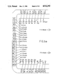
- FIG. 3 is an overall block diagram of an illustrative embodiment of a programmable logic device 10 constructed in accordance with the present invention.
- the major elements shown in this diagram are "fast inputs" 30, I/O pads 40, logic array blocks (LABs) 50, and programmable interconnect array (PIA) blocks 60.
- LABs logic array blocks
- POA programmable interconnect array
- Input signals into chip 10 come from either fast inputs 30 or I/O inputs 40.
- Fast inputs 30 are routed via lines 31 to all of LABs 50. These signals drive into the array portion of the LAB through buffers 57 which provide both the true and complement polarity of the signal presented to the fast input pad. These lines are called fast inputs because they go directly to the LABs, in contrast to I/O inputs 40 which go indirectly to the LABs via PIA blocks 60. This can be seen by following representative signal line 41 from the pads labeled I/O0:7 (which represent eight such I/O pads) to buffer 42. After the signal has been suitably buffered by buffer 42, it drives into the PIA along line 43.
- a signal which originated at one of the I/O pads 40 can be routed to any LAB 50 via the interconnect term 61 through buffer 58 and then into a true/complement LAB word line buffer 57.
- Signals propagating to an LAB via this path take additional time to traverse the PIA. Hence these signals are “slower” than the "fast” input lines 31 which go directly to the LAB as explained above. The reasons for providing these two different paths will be explained in due course.
- a typical LAB 50 will now be explained in more detail.
- this architecture there can be as many LABs as is deemed desirable.
- LABs for example, in various preferred embodiments implemented to date we have used either four or eight LABs.
- Each LAB 50 comprises macrocells 51 and expanders 52. Inputs to the LAB are provide by fast inputs via buffers 57, PIA inputs via interconnect terms 61 through buffers 58 and 57, feedback terms from macrocell outputs via buffers 54 and 57, and expander feedback terms via buffers 55 and 56.
- Two types of macrocells are provided. The only difference is the inclusion of output buffers 53 (plus their associated output enable (OE) signal 110 which provides the output tri-state control) in macrocells 1 through 8.
- Output buffers 53 selectively apply the associated macrocell outputs to I/O signal pins 40.
- Macrocells 9 through 16 have no associated output buffer and are therefore sometimes referred to as "buried" macrocells. In either case, the macrocells all have buffers 54 which take the signal generated by the macrocell and feed it to its own LAB (as described above) and also drive PIA word lines 62.
- each LAB 50 has 16 macrocells, 32 expanders, eight fast inputs, and 24 array inputs from the interconnect terms of the PIA.
- Each LAB also has a number of tri-stat output drivers 53: eight drivers 53 in the case of the LABs labelled group A, B, H, and G, and five drivers 53 in the case of the LABs labelled group C, D, F, and E. While we believe these choices to be optimum for the particular embodiment shown, other choices could be made without departing from the scope and spirit of the invention. For example, in another embodiment (shown in FIG. 7), there are four LABs, each of which has seven tri-state drivers In addition, the chip shown in FIG. 7 has eight dedicated inputs and four power/ground pins.
- the PIA provides a mechanism for programmably routing signals from I/O input pins 40 to any LAB and from any LAB macrocell output to any other LAB.
- the PIA includes word lines 43 and 62 and bit lines 61.
- the bit lines are also labelled “interconnect terms" in FIG. 3.
- there are 52 word lines 43 which come from the I/O lines, and there are 128 word lines 62 which are driven from macrocell buffers 54.
- Interconnect terms 61 are perpendicular to the word lines.
- programmable elements 63 which, when programmed in one state, provide a connection between the associated word and bit lines, and which, when programmed in the other state, provide no such connection.
- the programmable elements are EPROM transistors.
- other types of programmable elements such as EEPROM transistors, fuses, anti-fuses, or other similar elements could be used without departing from the scope and spirit of the invention.
- the entire PIA i.e., all of PIA blocks 60 taken together
- P-terms bit lines
- FIG. 4 Shown in the diagram of FIG. 4 are the groups of signals 530 and 531 going to the output buffers labeled 53 in FIG. 3. Lines 530 provide the path for data from the macrocells to the output buffers, and lines 531 provide the path for the output enable (OE) signals from the OE P-terms.
- the PIA block 60 associated with this LAB is shown as having 180 word lines and 24 bit lines as previously described.
- FIG. 5 we can see more of the detail of one of the macrocells. In this case it is shown with an I/O buffer 53. If it were a buried macrocell, the only difference (at least pictorially) would be the absence of output buffer 53, the OE P-term structure (101, 103, 110), and I/O pin 40.
- the programmable array is shown a the intersection of word lines 102 nd bit lines 101.
- the label 51 refers to that part labelled "macrocell” in FIG. 3, and the label 52 refers to that part labelled "expander” in FIG. 3.
- two expander P-terms are preferably grouped with the P-terms of each macrocell for convenience.
- the word "macrocell” will be used to describe the entire collection of P-terms (including the two expander P-terms) and the associated logic gates 103-107, flip-flop 123, and output buffer 53, if present.
- Each P-term receives inputs from the 128 word lines 102 (described earlier).
- There is a programmable element (similar to element 63 in the PIA) at the intersection of each bit line with each word line.
- a logical AND function of any of the word line variables can be formed by programming these elements. This is described in U.S. Pat. No. 4,617,479 and will not be repeated here.
- the correct logical outcome produced by each P-term is represented either as an active-low AND gate 103 or as a NOR gate 104.
- an active-high AND gate could be used if one notes that the opposite polarity word line were used as its input and thus achieve the same logical result.
- each P-term is as follows:
- the P-term labelled OE is used as the output enable for the associated output buffer 53. If this were a buried macrocell, this bit line would be absent.
- SETN is used to control the preset of flip-flop 123.
- P0, P1, and P2 feed OR gate 105 which produces a logical sum-of-products at its output 115.
- This collection of P-terms, in conjunction with gate 105 forms the "programmable AND, fixed OR" function described in U.S. Pat. No. 4,124,899.
- the term labeled INV is used as an "invert control" for XOR gate 107. This allows for the creation of inverted sum-of-product functions at line 121.
- the INV term can be used "dynamically" as a direct input to the XOR gate 107.
- any logic function which can be reduced to (1) an EXCLUSIVE-OR of an AND function with an AND-OR function, (2 ) an EXCLUSIVE-OR of an OR function with an OR-AND function, (3) an EXCLUSIVE-OR of an OR function with an AND-OR function, or (4) an EXCLUSIVE-OR of an AND function with an OR-AND function can be implemented in detail in FIGS. 8a and 8c; the dollar sign in FIG.
- EXCLUSIVE-OR function ACLK is used to create an "asynchronous" clock signal for flip-flop 123 in conjunction with gate 106 and gates 109 and 108.
- CLEARN is used to control the "Clear" line on flip-flop 123.
- EXP1 and EXP2 are the “expander” P-terms. Note that each expander 52 preferably includes only a single P-term.
- the present new architecture is a combination of three programmable ANDs, a fixed OR, and an XOR, with single-P-term "expanders".
- This architecture is believed to be superior to both the prior art structure shown in FIG. 2 and to the single-P-term architectures proposed in the above-mentioned Goetting et al. reference.
- the study bore this out and reached several other important conclusions. It was found that having less than three P-terms feeding the OR gate is very restrictive when doing counters and shift registers. For all other functions examined, three P-terms feeding the OR gate was always as good as four P-terms feeding the OR.
- Expanders 52 play an important role in this new architecture. As their name implies, these P-terms allow for growth. That is, they allow for implementation of those (less common) functions which do not fit within the three-P-term limit (for example, an 8-to-1 multiplexer can be fit into 9 expanders). Expander P-terms anywhere in the LAB can be used to form elements of these more complex functions, and then the outputs of these P-terms are combined using another P-term (typically one of the P-terms feeding a fixed OR gate 105) (see, for example, FIG. 8f). Functions formed with expander P-terms can also be used to feed other expanders on single P-terms such as INV, ACLK, SETN, CLEARN, or OE.
- FIG. 8e shows an example of a logic expression which requires more than three P-terms which can be factored into expressions which can be formed using the expander P-terms and recombined using another P-term (typically his will be a P-term which feeds the fixed OR gate).
- the original expression has been factored such that two factors are implemented in two expanders and then combined with the remainder of the expression in one of the P-terms feeding the fixed OR gate.
- the original expression was:
- the common factors X*Y are formed on the P-term feeding the fixed OR gate, while the remaining factors (A+B+C) and (D+E) are formed on each of two expanders and fed to the P-term which contains the X*Y term.
- an expression which would have required six P-terms to implement can now be done in three P-terms.
- either the expression (A+B+C) or the expression (D+E) were required by some other macrocell or macrocells.
- These same expressions formed on the expander P-terms could be used again by those other macrocells.
- an expression generated on the expanders can be amortized across all of the macrocells which have the expander's outputs as word line inputs.
- FIGS. 8a through 8g Latches require only two expanders. This structure is shown in FIG. 8h.
- XOR gate 107 receives its inputs from OR gate 105 and P-term INV.
- the logic signal on line 116 is 0, then the output of XOR gate 107 (line 121) will have the same logic value as input 115.
- line 116 is 1, then 121 Will be the logical inversion of 115.
- this structure in conjunction with a D flip-flop such as 123, also allows for emulating other flip-flop types such as T, J-K and R-S. Emulation of various flip-flop types using array logic and XOR gates is the subject of U.S. Pat. No. 4,677,318.
- the INV signal 116 needs to be set to a logic 1.
- Flip-flop block 123 appears to be a simple D flip-flop with active low preset (P) and clear (C). However, this is done for simplicity of illustration of the macrocell.
- the output signal 124 from flip-flop 123 (1) goes to the input of output driver 53, (2) feeds back (via buffer 54) to a word line driver 57 of its own LAB, and (3) drives one of the word lines of the PIA (indicated as line 62 in FIG. 3).
- This signal 124 can be used by any other LAB via its connection through the PIA.
- the signal also feeds a conventional tristate I/O buffer 53 such that if the buffer is enabled by line 110, the signal from 124 will drive off chip through I/O pin 40.
- I/O pin 40 can also provide an input path from off chip via line 41.
- This line drives buffer 42 (FIG. 3) whose output becomes one of the word lines for the PIA shown as line 43 in FIG. 3.
- I/O buffer 53 can be dynamically controlled by the OE P-term, in which case pin 40 may be both an input and an output depending upon the state of line 110. Alternatively, by programming the chip such that OE is always 0 buffer 53 will always be disabled, in which case I/O pin 40 can be used permanently as an input. Thus each of I/O pins 40 can be configured as input, output, or bi-directional input/output terminals. Because of the feedback of signal 124 to the LAB and the PIA, and the I/O input line 41, disabling of the output driver 53 does not result in the loss of the macrocell's functionality. This is a significant advantage over some prior art devices.
- this structure includes inverter 109, AND gate 108, OR gate 106, and P-term ACLK.
- Inverter 109 AND gate 108
- OR gate 106 OR gate 106
- P-term ACLK Three modes of operation are anticipated as follows:
- ECKN which is an extra P-term (not shown) in the LAB
- line 125 is logic 0.
- line 122 is directly controlled by the state of the ACLK P-term.
- ACLK can be any (inputs active-low) AND function of any of the word line variables.
- Each flip-flop in the LAB has its own separate (“asynchronous") P-term clock.
- ECKN is programmed to be 0 and thus ECK is 1. This allows the signal EXT.(SYNC.)CLK. on line 32 to propagate through AND gate 108 and appear on line 125. EXT.(SYNC.)CLK. line 32 comes from an input pad (one of the "fast inputs") not shown. This signal on line 125 passes through OR gate 106 and appears on line 122. In this way, an external signal can directly control the clocking of flip-flop 123. Because there is a single ECKN P-term per LAB, the selection of synchronous mode is done on a per LAB basis rather than on a per macrocell basis.
- FIG. 6a illustrates one way in which the chip of FIG. 3 can be bonded out to 68 pins
- FIG. 6b shows how the same chip can be bonded out to 40 pins.
- the chip pads which are not bonded out in FIG. 6b are certain I/O pins.
- the "output" signals that could be applied to these chip pads are still usable internally, and the remaining external inputs can be applied to any LAB via PIA 60.
- the only loss in chip capability is the loss of the external chip I/O connections.
- the eight LABs on the chip are designated A through H.
- the eight I/O pads I/OA0-8 of LAB A are bonded out to lead tips 11 through 4, respectively, while in FIG. 6b only four I/O pads I/OA0, 1, 2, and 7 are bonded out to lead tips 37 through 34, respectively.
- LABs A, D, E, and H each have eight bonded-out I/O pads and the remaining LABs each have five bonded-out I/O pads.
- LABs A, D, E, and H each have four bonded-out I/O pads and the remaining I/O pads each have three bonded-out I/O pads.
- the "fast" inputs are designated I0 through I7.
Abstract
Description
FUNCTION=A*D*X*Y+A*E*X*Y+B*D*X*Y+B*E*X*Y+C*D*X*Y+C*E*X*Y
FUNCTION=(X*Y)*(A+B+C)*(D+E)
Claims (2)
Priority Applications (1)
| Application Number | Priority Date | Filing Date | Title |
|---|---|---|---|
| US07/407,411 US4912342A (en) | 1988-05-05 | 1989-09-14 | Programmable logic device with array blocks with programmable clocking |
Applications Claiming Priority (2)
| Application Number | Priority Date | Filing Date | Title |
|---|---|---|---|
| US07/190,663 US4871930A (en) | 1988-05-05 | 1988-05-05 | Programmable logic device with array blocks connected via programmable interconnect |
| US07/407,411 US4912342A (en) | 1988-05-05 | 1989-09-14 | Programmable logic device with array blocks with programmable clocking |
Related Parent Applications (1)
| Application Number | Title | Priority Date | Filing Date |
|---|---|---|---|
| US07/190,663 Division US4871930A (en) | 1988-05-05 | 1988-05-05 | Programmable logic device with array blocks connected via programmable interconnect |
Publications (1)
| Publication Number | Publication Date |
|---|---|
| US4912342A true US4912342A (en) | 1990-03-27 |
Family
ID=26886315
Family Applications (1)
| Application Number | Title | Priority Date | Filing Date |
|---|---|---|---|
| US07/407,411 Expired - Lifetime US4912342A (en) | 1988-05-05 | 1989-09-14 | Programmable logic device with array blocks with programmable clocking |
Country Status (1)
| Country | Link |
|---|---|
| US (1) | US4912342A (en) |
Cited By (140)
| Publication number | Priority date | Publication date | Assignee | Title |
|---|---|---|---|---|
| US5046035A (en) * | 1987-08-26 | 1991-09-03 | Ict International Cmos Tech., Inc. | High-performance user programmable logic device (PLD) |
| US5053647A (en) * | 1989-07-17 | 1991-10-01 | Fuji Photo Film Co., Ltd. | Programmable logic array having feedback flip-flops connected between a product array's inputs and its outputs |
| US5091661A (en) * | 1990-09-24 | 1992-02-25 | Altera Corporation | Methods and apparatus for reducing coupling noise in programmable logic devices |
| US5151623A (en) * | 1985-03-29 | 1992-09-29 | Advanced Micro Devices, Inc. | Programmable logic device with multiple, flexible asynchronous programmable logic blocks interconnected by a high speed switch matrix |
| US5155393A (en) * | 1991-09-06 | 1992-10-13 | Atmel Corporation | Clock selection for storage elements of integrated circuits |
| WO1992020155A1 (en) * | 1991-05-06 | 1992-11-12 | Lattice Semiconductor Corporation | Output logic macrocell with enhanced functional capabilities |
| US5189320A (en) * | 1991-09-23 | 1993-02-23 | Atmel Corporation | Programmable logic device with multiple shared logic arrays |
| US5204555A (en) * | 1990-04-05 | 1993-04-20 | Gazelle Microcircuits, Inc. | Logic array having high frequency internal clocking |
| US5218240A (en) * | 1990-11-02 | 1993-06-08 | Concurrent Logic, Inc. | Programmable logic cell and array with bus repeaters |
| US5384499A (en) * | 1991-04-25 | 1995-01-24 | Altera Corporation | High-density erasable programmable logic device architecture using multiplexer interconnections |
| US5436514A (en) * | 1985-03-29 | 1995-07-25 | Advanced Micro Devices, Inc. | High speed centralized switch matrix for a programmable logic device |
| US5451887A (en) * | 1986-09-19 | 1995-09-19 | Actel Corporation | Programmable logic module and architecture for field programmable gate array device |
| US5483178A (en) * | 1993-03-29 | 1996-01-09 | Altera Corporation | Programmable logic device with logic block outputs coupled to adjacent logic block output multiplexers |
| US5485103A (en) * | 1991-09-03 | 1996-01-16 | Altera Corporation | Programmable logic array with local and global conductors |
| US5485102A (en) * | 1992-11-19 | 1996-01-16 | Altera Corporation | Programmable logic devices with spare circuits for replacement of defects |
| US5510730A (en) | 1986-09-19 | 1996-04-23 | Actel Corporation | Reconfigurable programmable interconnect architecture |
| US5525917A (en) * | 1994-12-16 | 1996-06-11 | Altera Corporation | Sense amplifier with feedback and stabilization |
| US5530378A (en) * | 1995-04-26 | 1996-06-25 | Xilinx, Inc. | Cross point interconnect structure with reduced area |
| US5537057A (en) * | 1995-02-14 | 1996-07-16 | Altera Corporation | Programmable logic array device with grouped logic regions and three types of conductors |
| US5543732A (en) * | 1995-05-17 | 1996-08-06 | Altera Corporation | Programmable logic array devices with interconnect lines of various lengths |
| US5543730A (en) * | 1995-05-17 | 1996-08-06 | Altera Corporation | Techniques for programming programmable logic array devices |
| US5565793A (en) * | 1995-08-22 | 1996-10-15 | Altera Corporation | Programmable logic array integrated circuit devices with regions of enhanced interconnectivity |
| US5581501A (en) * | 1995-08-17 | 1996-12-03 | Altera Corporation | Nonvolatile SRAM cells and cell arrays |
| US5592106A (en) * | 1995-05-17 | 1997-01-07 | Altera Corporation | Programmable logic array integrated circuits with interconnection conductors of overlapping extent |
| US5592102A (en) * | 1995-10-19 | 1997-01-07 | Altera Corporation | Means and apparatus to minimize the effects of silicon processing defects in programmable logic devices |
| US5594366A (en) * | 1994-05-04 | 1997-01-14 | Atmel Corporation | Programmable logic device with regional and universal signal routing |
| US5606267A (en) * | 1986-09-19 | 1997-02-25 | Actel Corporation | Programmable logic module and architecture for field programmable gate array device |
| US5610534A (en) * | 1990-05-11 | 1997-03-11 | Actel Corporation | Logic module for a programmable logic device |
| US5614840A (en) * | 1995-05-17 | 1997-03-25 | Altera Corporation | Programmable logic array integrated circuits with segmented, selectively connectable, long interconnection conductors |
| US5631576A (en) * | 1995-09-01 | 1997-05-20 | Altera Corporation | Programmable logic array integrated circuit devices with flexible carry chains |
| US5635856A (en) * | 1995-10-03 | 1997-06-03 | Cypress Semiconductor Corporation | High speed programmable macrocell with combined path for storage and combinatorial modes |
| US5638008A (en) * | 1995-10-30 | 1997-06-10 | Cypress Semiconductor Corp. | Method and apparatus for generating an asynchronously clocked signal in a synchronously clocked programmable device |
| US5659717A (en) * | 1995-07-31 | 1997-08-19 | Altera Corporation | Methods for partitioning circuits in order to allocate elements among multiple circuit groups |
| US5670895A (en) * | 1995-10-19 | 1997-09-23 | Altera Corporation | Routing connections for programmable logic array integrated circuits |
| US5672985A (en) * | 1995-12-18 | 1997-09-30 | Altera Corporation | Programmable logic array integrated circuits with carry and/or cascade rings |
| US5689195A (en) * | 1995-05-17 | 1997-11-18 | Altera Corporation | Programmable logic array integrated circuit devices |
| US5691653A (en) * | 1996-01-16 | 1997-11-25 | Altera Corporation | Product term based programmable logic array devices with reduced control memory requirements |
| US5694058A (en) * | 1996-03-20 | 1997-12-02 | Altera Corporation | Programmable logic array integrated circuits with improved interconnection conductor utilization |
| US5703498A (en) * | 1995-06-02 | 1997-12-30 | International Business Machines Corporation | Programmable array clock/reset resource |
| US5729495A (en) * | 1995-09-29 | 1998-03-17 | Altera Corporation | Dynamic nonvolatile memory cell |
| US5744991A (en) * | 1995-10-16 | 1998-04-28 | Altera Corporation | System for distributing clocks using a delay lock loop in a programmable logic circuit |
| US5764080A (en) * | 1995-08-24 | 1998-06-09 | Altera Corporation | Input/output interface circuitry for programmable logic array integrated circuit devices |
| US5768372A (en) * | 1996-03-13 | 1998-06-16 | Altera Corporation | Method and apparatus for securing programming data of a programmable logic device |
| US5767734A (en) * | 1995-12-21 | 1998-06-16 | Altera Corporation | High-voltage pump with initiation scheme |
| US5771264A (en) * | 1996-08-29 | 1998-06-23 | Altera Corporation | Digital delay lock loop for clock signal frequency multiplication |
| US5793246A (en) * | 1995-11-08 | 1998-08-11 | Altera Corporation | High voltage pump scheme incorporating an overlapping clock |
| US5815726A (en) * | 1994-11-04 | 1998-09-29 | Altera Corporation | Coarse-grained look-up table architecture |
| US5821773A (en) * | 1995-09-06 | 1998-10-13 | Altera Corporation | Look-up table based logic element with complete permutability of the inputs to the secondary signals |
| US5825072A (en) * | 1993-07-07 | 1998-10-20 | Actel Corporation | Circuits for ESD Protection of metal to-metal antifuses during processing |
| US5835998A (en) * | 1996-04-04 | 1998-11-10 | Altera Corporation | Logic cell for programmable logic devices |
| US5844854A (en) * | 1996-09-18 | 1998-12-01 | Altera Corporation | Programmable logic device with two dimensional memory addressing |
| US5850365A (en) * | 1994-12-16 | 1998-12-15 | Altera Corporation | Sense amplifier with individually optimized high and low power modes |
| US5869979A (en) * | 1996-04-05 | 1999-02-09 | Altera Corporation | Technique for preconditioning I/Os during reconfiguration |
| US5872463A (en) * | 1996-04-04 | 1999-02-16 | Altera Corporation | Routing in programmable logic devices using shared distributed programmable logic connectors |
| US5880597A (en) * | 1996-09-18 | 1999-03-09 | Altera Corporation | Interleaved interconnect for programmable logic array devices |
| US5894228A (en) * | 1996-01-10 | 1999-04-13 | Altera Corporation | Tristate structures for programmable logic devices |
| US5900743A (en) * | 1995-05-17 | 1999-05-04 | Altera Corporation | Programmable logic array devices with interconnect lines of various lengths |
| US5909126A (en) * | 1995-05-17 | 1999-06-01 | Altera Corporation | Programmable logic array integrated circuit devices with interleaved logic array blocks |
| US5914904A (en) * | 1996-10-01 | 1999-06-22 | Altera Corporation | Compact electrically erasable memory cells and arrays |
| US5923868A (en) * | 1994-07-29 | 1999-07-13 | Cypress Semiconductor Corp. | Methods for maximizing routability in a programmable interconnect matrix having less than full connectability |
| US5936425A (en) * | 1995-05-17 | 1999-08-10 | Altera Corporation | Tri-statable input/output circuitry for programmable logic |
| US5936426A (en) * | 1997-02-03 | 1999-08-10 | Actel Corporation | Logic function module for field programmable array |
| US5939790A (en) * | 1996-04-09 | 1999-08-17 | Altera Corporation | Integrated circuit pad structures |
| US5942914A (en) * | 1996-10-25 | 1999-08-24 | Altera Corporation | PLD with split multiplexed inputs from global conductors |
| US5949710A (en) * | 1996-04-10 | 1999-09-07 | Altera Corporation | Programmable interconnect junction |
| US5959891A (en) * | 1996-08-16 | 1999-09-28 | Altera Corporation | Evaluation of memory cell characteristics |
| US5963049A (en) * | 1995-05-17 | 1999-10-05 | Altera Corporation | Programmable logic array integrated circuit architectures |
| US5970255A (en) * | 1995-10-16 | 1999-10-19 | Altera Corporation | System for coupling programmable logic device to external circuitry which selects a logic standard and uses buffers to modify output and input signals accordingly |
| US5977791A (en) * | 1996-04-15 | 1999-11-02 | Altera Corporation | Embedded memory block with FIFO mode for programmable logic device |
| US5977793A (en) * | 1996-10-10 | 1999-11-02 | Altera Corporation | Programmable logic device with hierarchical interconnection resources |
| US5982195A (en) * | 1997-02-20 | 1999-11-09 | Altera Corporation | Programmable logic device architectures |
| US5986465A (en) * | 1996-04-09 | 1999-11-16 | Altera Corporation | Programmable logic integrated circuit architecture incorporating a global shareable expander |
| US5998295A (en) * | 1996-04-10 | 1999-12-07 | Altera Corporation | Method of forming a rough region on a substrate |
| US5999016A (en) * | 1996-10-10 | 1999-12-07 | Altera Corporation | Architectures for programmable logic devices |
| US5999015A (en) * | 1997-02-20 | 1999-12-07 | Altera Corporation | Logic region resources for programmable logic devices |
| US6005806A (en) * | 1996-03-14 | 1999-12-21 | Altera Corporation | Nonvolatile configuration cells and cell arrays |
| US6018476A (en) * | 1996-09-16 | 2000-01-25 | Altera Corporation | Nonvolatile configuration cells and cell arrays |
| US6025737A (en) * | 1996-11-27 | 2000-02-15 | Altera Corporation | Circuitry for a low internal voltage integrated circuit |
| US6028446A (en) * | 1995-06-06 | 2000-02-22 | Advanced Micro Devices, Inc. | Flexible synchronous and asynchronous circuits for a very high density programmable logic device |
| US6034540A (en) * | 1997-04-08 | 2000-03-07 | Altera Corporation | Programmable logic integrated circuit architecture incorporating a lonely register |
| US6034536A (en) * | 1997-02-05 | 2000-03-07 | Altera Corporation | Redundancy circuitry for logic circuits |
| US6045252A (en) * | 1996-02-20 | 2000-04-04 | Altera Corporation | Methods for allocating circuit design portions among physical circuit portions |
| US6052327A (en) * | 1997-10-14 | 2000-04-18 | Altera Corporation | Dual-port programmable logic device variable depth and width memory array |
| US6084427A (en) * | 1998-05-19 | 2000-07-04 | Altera Corporation | Programmable logic devices with enhanced multiplexing capabilities |
| US6091258A (en) * | 1997-02-05 | 2000-07-18 | Altera Corporation | Redundancy circuitry for logic circuits |
| US6097212A (en) * | 1997-10-09 | 2000-08-01 | Lattice Semiconductor Corporation | Variable grain architecture for FPGA integrated circuits |
| US6107824A (en) * | 1997-10-16 | 2000-08-22 | Altera Corporation | Circuitry and methods for internal interconnection of programmable logic devices |
| US6107822A (en) * | 1996-04-09 | 2000-08-22 | Altera Corporation | Logic element for a programmable logic integrated circuit |
| US6107820A (en) * | 1997-05-23 | 2000-08-22 | Altera Corporation | Redundancy circuitry for programmable logic devices with interleaved input circuits |
| US6107825A (en) * | 1997-10-16 | 2000-08-22 | Altera Corporation | Input/output circuitry for programmable logic devices |
| US6118302A (en) * | 1996-05-28 | 2000-09-12 | Altera Corporation | Interface for low-voltage semiconductor devices |
| US6121790A (en) * | 1997-10-16 | 2000-09-19 | Altera Corporation | Programmable logic device with enhanced multiplexing capabilities in interconnect resources |
| US6127844A (en) * | 1997-02-20 | 2000-10-03 | Altera Corporation | PCI-compatible programmable logic devices |
| US6127843A (en) * | 1997-12-22 | 2000-10-03 | Vantis Corporation | Dual port SRAM memory for run time use in FPGA integrated circuits |
| US6130551A (en) * | 1998-01-19 | 2000-10-10 | Vantis Corporation | Synthesis-friendly FPGA architecture with variable length and variable timing interconnect |
| US6130555A (en) * | 1997-10-13 | 2000-10-10 | Altera Corporation | Driver circuitry for programmable logic devices |
| US6133750A (en) * | 1998-04-27 | 2000-10-17 | Lattice Semiconductor Corp. | Combination of global clock and localized clocks |
| US6181162B1 (en) | 1994-04-10 | 2001-01-30 | Altera Corporation | Programmable logic device with highly routable interconnect |
| US6184707B1 (en) | 1998-10-07 | 2001-02-06 | Altera Corporation | Look-up table based logic element with complete permutability of the inputs to the secondary signals |
| US6184710B1 (en) | 1997-03-20 | 2001-02-06 | Altera Corporation | Programmable logic array devices with enhanced interconnectivity between adjacent logic regions |
| US6184706B1 (en) | 1996-04-05 | 2001-02-06 | Altera Corporation | Logic device architecture and method of operation |
| US6191998B1 (en) | 1997-10-16 | 2001-02-20 | Altera Corporation | Programmable logic device memory array circuit having combinable single-port memory arrays |
| US6201404B1 (en) | 1998-07-14 | 2001-03-13 | Altera Corporation | Programmable logic device with redundant circuitry |
| US6236597B1 (en) | 1996-09-16 | 2001-05-22 | Altera Corporation | Nonvolatile memory cell with multiple gate oxide thicknesses |
| US6239612B1 (en) | 1997-08-20 | 2001-05-29 | Altera Corporation | Programmable I/O cells with multiple drivers |
| US6243664B1 (en) | 1998-10-27 | 2001-06-05 | Cypress Semiconductor Corporation | Methods for maximizing routability in a programmable interconnect matrix having less than full connectability |
| US6255850B1 (en) | 1997-10-28 | 2001-07-03 | Altera Corporation | Integrated circuit with both clamp protection and high impedance protection from input overshoot |
| US6288970B1 (en) | 1997-10-16 | 2001-09-11 | Altera Corporation | Programmable logic device memory array circuit having combinable single-port memory arrays |
| US6300794B1 (en) | 1996-10-10 | 2001-10-09 | Altera Corporation | Programmable logic device with hierarchical interconnection resources |
| US6320412B1 (en) | 1999-12-20 | 2001-11-20 | Btr, Inc. C/O Corporate Trust Co. | Architecture and interconnect for programmable logic circuits |
| US6384630B2 (en) | 1996-06-05 | 2002-05-07 | Altera Corporation | Techniques for programming programmable logic array devices |
| US6407576B1 (en) | 1999-03-04 | 2002-06-18 | Altera Corporation | Interconnection and input/output resources for programmable logic integrated circuit devices |
| US6462578B2 (en) * | 1993-08-03 | 2002-10-08 | Btr, Inc. | Architecture and interconnect scheme for programmable logic circuits |
| US6480028B2 (en) | 1998-11-18 | 2002-11-12 | Altera Corporation | Programmable logic device architectures with super-regions having logic regions and memory region |
| US6507217B2 (en) | 1993-08-03 | 2003-01-14 | Btr, Inc. | Architecture and interconnect scheme for programmable logic circuits |
| US6507216B1 (en) | 1998-11-18 | 2003-01-14 | Altera Corporation | Efficient arrangement of interconnection resources on programmable logic devices |
| US6759870B2 (en) | 1991-09-03 | 2004-07-06 | Altera Corporation | Programmable logic array integrated circuits |
| US20040182059A1 (en) * | 2002-07-19 | 2004-09-23 | Mark Bland | Hinge system for articulating mower decks |
| USRE38651E1 (en) * | 1994-05-18 | 2004-11-09 | Altera Corporation | Variable depth and width memory device |
| US6882177B1 (en) | 1996-01-10 | 2005-04-19 | Altera Corporation | Tristate structures for programmable logic devices |
| US20050184753A1 (en) * | 2000-03-06 | 2005-08-25 | Actel Corporation, A California Corporation | Block level routing architecture in a field programmable gate array |
| US20050218928A1 (en) * | 2004-03-30 | 2005-10-06 | Pani Peter M | Scalable non-blocking switching network for programmable logic |
| US20060023704A1 (en) * | 2004-07-29 | 2006-02-02 | Pani Peter M | Interconnection fabric using switching networks in hierarchy |
| US6996736B1 (en) | 2001-05-06 | 2006-02-07 | Altera Corporation | Programmable clock network for distributing clock signals to and between first and second sections of an integrated circuit |
| US7111110B1 (en) | 2002-12-10 | 2006-09-19 | Altera Corporation | Versatile RAM for programmable logic device |
| US7148722B1 (en) | 1997-02-20 | 2006-12-12 | Altera Corporation | PCI-compatible programmable logic devices |
| USRE40423E1 (en) | 1996-07-29 | 2008-07-08 | Xilinx, Inc. | Multiport RAM with programmable data port configuration |
| US7423453B1 (en) | 2006-01-20 | 2008-09-09 | Advantage Logic, Inc. | Efficient integrated circuit layout scheme to implement a scalable switching network used in interconnection fabric |
| US20080278678A1 (en) * | 2003-10-09 | 2008-11-13 | Howell Thomas A | Eyeglasses with user monitoring |
| US7484081B1 (en) | 2000-10-10 | 2009-01-27 | Altera Corporation | Method and apparatus for protecting designs in SRAM-based programmable logic devices |
| US20100186010A1 (en) * | 2009-01-16 | 2010-07-22 | International Business Machines Corporation | Dynamic Checking of Hardware Resources for Virtual Environments |
| US20100327907A1 (en) * | 2009-06-24 | 2010-12-30 | Ting Benjamin S | Enhanced permutable switching network with multicasting signals for interconnection fabric |
| US7893772B1 (en) | 2007-12-03 | 2011-02-22 | Cypress Semiconductor Corporation | System and method of loading a programmable counter |
| US8461863B2 (en) | 2011-04-29 | 2013-06-11 | Altera Corporation | Method and apparatus for securing a programmable device using a kill switch |
| US8566616B1 (en) | 2004-09-10 | 2013-10-22 | Altera Corporation | Method and apparatus for protecting designs in SRAM-based programmable logic devices and the like |
| US8612772B1 (en) | 2004-09-10 | 2013-12-17 | Altera Corporation | Security core using soft key |
| US8627105B2 (en) | 2011-04-29 | 2014-01-07 | Altera Corporation | Method and apparatus for securing programming data of a programmable device |
| US8719957B2 (en) | 2011-04-29 | 2014-05-06 | Altera Corporation | Systems and methods for detecting and mitigating programmable logic device tampering |
| US8736299B1 (en) | 2011-04-29 | 2014-05-27 | Altera Corporation | Setting security features of programmable logic devices |
| US9026873B2 (en) | 2013-07-23 | 2015-05-05 | Altera Coporation | Method and apparatus for securing configuration scan chains of a programmable device |
Citations (20)
| Publication number | Priority date | Publication date | Assignee | Title |
|---|---|---|---|---|
| US3566153A (en) * | 1969-04-30 | 1971-02-23 | Texas Instruments Inc | Programmable sequential logic |
| US4124899A (en) * | 1977-05-23 | 1978-11-07 | Monolithic Memories, Inc. | Programmable array logic circuit |
| US4269562A (en) * | 1978-08-07 | 1981-05-26 | Burgess James B | Trench trash compactor |
| US4494021A (en) * | 1982-08-30 | 1985-01-15 | Xerox Corporation | Self-calibrated clock and timing signal generator for MOS/VLSI circuitry |
| US4525641A (en) * | 1982-12-10 | 1985-06-25 | International Business Machines Corporation | Flip-flop programmer using cascaded logic arrays |
| US4554640A (en) * | 1984-01-30 | 1985-11-19 | Monolithic Memories, Inc. | Programmable array logic circuit with shared product terms |
| US4609986A (en) * | 1984-06-14 | 1986-09-02 | Altera Corporation | Programmable logic array device using EPROM technology |
| US4611133A (en) * | 1983-05-12 | 1986-09-09 | Codex Corporation | High speed fully precharged programmable logic array |
| US4617479A (en) * | 1984-05-03 | 1986-10-14 | Altera Corporation | Programmable logic array device using EPROM technology |
| US4644191A (en) * | 1985-09-19 | 1987-02-17 | Harris Corporation | Programmable array logic with shared product terms |
| US4677318A (en) * | 1985-04-12 | 1987-06-30 | Altera Corporation | Programmable logic storage element for programmable logic devices |
| US4687959A (en) * | 1986-03-27 | 1987-08-18 | Motorola, Inc. | Method and apparatus for access to a PLA |
| US4689654A (en) * | 1985-04-19 | 1987-08-25 | Nixdorf Computer Ag | Logic array chip |
| US4697105A (en) * | 1986-07-23 | 1987-09-29 | American Telephone And Telegraph Company, At&T Bell Laboratories | CMOS programmable logic array |
| US4703206A (en) * | 1985-11-19 | 1987-10-27 | Signetics Corporation | Field-programmable logic device with programmable foldback to control number of logic levels |
| US4713792A (en) * | 1985-06-06 | 1987-12-15 | Altera Corporation | Programmable macrocell using eprom or eeprom transistors for architecture control in programmable logic circuits |
| US4740721A (en) * | 1985-10-21 | 1988-04-26 | Western Digital Corporation | Programmable logic array with single clock dynamic logic |
| US4758746A (en) * | 1985-08-12 | 1988-07-19 | Monolithic Memories, Inc. | Programmable logic array with added array of gates and added output routing flexibility |
| US4764691A (en) * | 1985-10-15 | 1988-08-16 | American Microsystems, Inc. | CMOS programmable logic array using NOR gates for clocking |
| US4812685A (en) * | 1987-02-12 | 1989-03-14 | Bull, S.A. | Dynamic logic array with isolation and latching means between planes |
-
1989
- 1989-09-14 US US07/407,411 patent/US4912342A/en not_active Expired - Lifetime
Patent Citations (22)
| Publication number | Priority date | Publication date | Assignee | Title |
|---|---|---|---|---|
| US3566153A (en) * | 1969-04-30 | 1971-02-23 | Texas Instruments Inc | Programmable sequential logic |
| US4124899A (en) * | 1977-05-23 | 1978-11-07 | Monolithic Memories, Inc. | Programmable array logic circuit |
| US4124899B1 (en) * | 1977-05-23 | 1987-04-28 | ||
| US4269562A (en) * | 1978-08-07 | 1981-05-26 | Burgess James B | Trench trash compactor |
| US4494021A (en) * | 1982-08-30 | 1985-01-15 | Xerox Corporation | Self-calibrated clock and timing signal generator for MOS/VLSI circuitry |
| US4525641A (en) * | 1982-12-10 | 1985-06-25 | International Business Machines Corporation | Flip-flop programmer using cascaded logic arrays |
| US4611133A (en) * | 1983-05-12 | 1986-09-09 | Codex Corporation | High speed fully precharged programmable logic array |
| US4554640A (en) * | 1984-01-30 | 1985-11-19 | Monolithic Memories, Inc. | Programmable array logic circuit with shared product terms |
| US4617479A (en) * | 1984-05-03 | 1986-10-14 | Altera Corporation | Programmable logic array device using EPROM technology |
| US4617479B1 (en) * | 1984-05-03 | 1993-09-21 | Altera Semiconductor Corp. | Programmable logic array device using eprom technology |
| US4609986A (en) * | 1984-06-14 | 1986-09-02 | Altera Corporation | Programmable logic array device using EPROM technology |
| US4677318A (en) * | 1985-04-12 | 1987-06-30 | Altera Corporation | Programmable logic storage element for programmable logic devices |
| US4689654A (en) * | 1985-04-19 | 1987-08-25 | Nixdorf Computer Ag | Logic array chip |
| US4713792A (en) * | 1985-06-06 | 1987-12-15 | Altera Corporation | Programmable macrocell using eprom or eeprom transistors for architecture control in programmable logic circuits |
| US4758746A (en) * | 1985-08-12 | 1988-07-19 | Monolithic Memories, Inc. | Programmable logic array with added array of gates and added output routing flexibility |
| US4644191A (en) * | 1985-09-19 | 1987-02-17 | Harris Corporation | Programmable array logic with shared product terms |
| US4764691A (en) * | 1985-10-15 | 1988-08-16 | American Microsystems, Inc. | CMOS programmable logic array using NOR gates for clocking |
| US4740721A (en) * | 1985-10-21 | 1988-04-26 | Western Digital Corporation | Programmable logic array with single clock dynamic logic |
| US4703206A (en) * | 1985-11-19 | 1987-10-27 | Signetics Corporation | Field-programmable logic device with programmable foldback to control number of logic levels |
| US4687959A (en) * | 1986-03-27 | 1987-08-18 | Motorola, Inc. | Method and apparatus for access to a PLA |
| US4697105A (en) * | 1986-07-23 | 1987-09-29 | American Telephone And Telegraph Company, At&T Bell Laboratories | CMOS programmable logic array |
| US4812685A (en) * | 1987-02-12 | 1989-03-14 | Bull, S.A. | Dynamic logic array with isolation and latching means between planes |
Non-Patent Citations (6)
| Title |
|---|
| E. Goetting et al., "A CMOS Electrically-Reprogrammable ASIC with Multi-Level Random Logic Capabilities," 1986 IEEE International Solid-State Circuits Conference, pp. 244-245 and 359-360, 1986. |
| E. Goetting et al., A CMOS Electrically Reprogrammable ASIC with Multi Level Random Logic Capabilities, 1986 IEEE International Solid State Circuits Conference, pp. 244 245 and 359 360, 1986. * |
| J. C. Leininger, "Universal Logic Module," IBM Technical Disclosure Bulletin, vol. 13, No. 5, pp. 1294-1295, Oct. 1970. |
| J. C. Leininger, Universal Logic Module, IBM Technical Disclosure Bulletin, vol. 13, No. 5, pp. 1294 1295, Oct. 1970. * |
| R. R. Munoz et al., "Automatic Partitioning of Programmable Logic Devices," VLSI Systems Design, Oct. 1987, pp. 74-76, 78, and 86. |
| R. R. Munoz et al., Automatic Partitioning of Programmable Logic Devices, VLSI Systems Design, Oct. 1987, pp. 74 76, 78, and 86. * |
Cited By (293)
| Publication number | Priority date | Publication date | Assignee | Title |
|---|---|---|---|---|
| US5764078A (en) * | 1985-03-29 | 1998-06-09 | Advanced Micro Devices, Inc. | Family of multiple segmented programmable logic blocks interconnected by a high speed centralized switch matrix |
| US5151623A (en) * | 1985-03-29 | 1992-09-29 | Advanced Micro Devices, Inc. | Programmable logic device with multiple, flexible asynchronous programmable logic blocks interconnected by a high speed switch matrix |
| US5612631A (en) * | 1985-03-29 | 1997-03-18 | Advanced Micro Devices, Inc. | An I/O macrocell for a programmable logic device |
| US5869981A (en) * | 1985-03-29 | 1999-02-09 | Advanced Micro Devices, Inc. | High density programmable logic device |
| US5436514A (en) * | 1985-03-29 | 1995-07-25 | Advanced Micro Devices, Inc. | High speed centralized switch matrix for a programmable logic device |
| US6160420A (en) | 1986-09-19 | 2000-12-12 | Actel Corporation | Programmable interconnect architecture |
| US5698992A (en) * | 1986-09-19 | 1997-12-16 | Actel Corporation | Programmable logic module and architecture for field programmable gate array device |
| US5606267A (en) * | 1986-09-19 | 1997-02-25 | Actel Corporation | Programmable logic module and architecture for field programmable gate array device |
| US5510730A (en) | 1986-09-19 | 1996-04-23 | Actel Corporation | Reconfigurable programmable interconnect architecture |
| US5570041A (en) * | 1986-09-19 | 1996-10-29 | Actel Corporation | Programmable logic module and architecture for field programmable gate array device |
| US5451887A (en) * | 1986-09-19 | 1995-09-19 | Actel Corporation | Programmable logic module and architecture for field programmable gate array device |
| US5046035A (en) * | 1987-08-26 | 1991-09-03 | Ict International Cmos Tech., Inc. | High-performance user programmable logic device (PLD) |
| US5053647A (en) * | 1989-07-17 | 1991-10-01 | Fuji Photo Film Co., Ltd. | Programmable logic array having feedback flip-flops connected between a product array's inputs and its outputs |
| US5204555A (en) * | 1990-04-05 | 1993-04-20 | Gazelle Microcircuits, Inc. | Logic array having high frequency internal clocking |
| USRE35797E (en) * | 1990-04-05 | 1998-05-19 | Triquint Semiconductor, Inc. | Logic array having high frequency internal clocking |
| US5610534A (en) * | 1990-05-11 | 1997-03-11 | Actel Corporation | Logic module for a programmable logic device |
| US5781033A (en) * | 1990-05-11 | 1998-07-14 | Actel Corporation | Logic module with configurable combinational and sequential blocks |
| US5091661A (en) * | 1990-09-24 | 1992-02-25 | Altera Corporation | Methods and apparatus for reducing coupling noise in programmable logic devices |
| US5218240A (en) * | 1990-11-02 | 1993-06-08 | Concurrent Logic, Inc. | Programmable logic cell and array with bus repeaters |
| US5384499A (en) * | 1991-04-25 | 1995-01-24 | Altera Corporation | High-density erasable programmable logic device architecture using multiplexer interconnections |
| US5557217A (en) * | 1991-04-25 | 1996-09-17 | Altera Corporation | High-density erasable programmable logic device architecture using multiplexer interconnections |
| US5191243A (en) * | 1991-05-06 | 1993-03-02 | Lattice Semiconductor Corporation | Output logic macrocell with enhanced functional capabilities |
| WO1992020155A1 (en) * | 1991-05-06 | 1992-11-12 | Lattice Semiconductor Corporation | Output logic macrocell with enhanced functional capabilities |
| US5485103A (en) * | 1991-09-03 | 1996-01-16 | Altera Corporation | Programmable logic array with local and global conductors |
| US6759870B2 (en) | 1991-09-03 | 2004-07-06 | Altera Corporation | Programmable logic array integrated circuits |
| US5155393A (en) * | 1991-09-06 | 1992-10-13 | Atmel Corporation | Clock selection for storage elements of integrated circuits |
| US5189320A (en) * | 1991-09-23 | 1993-02-23 | Atmel Corporation | Programmable logic device with multiple shared logic arrays |
| US5485102A (en) * | 1992-11-19 | 1996-01-16 | Altera Corporation | Programmable logic devices with spare circuits for replacement of defects |
| US5483178A (en) * | 1993-03-29 | 1996-01-09 | Altera Corporation | Programmable logic device with logic block outputs coupled to adjacent logic block output multiplexers |
| US5825072A (en) * | 1993-07-07 | 1998-10-20 | Actel Corporation | Circuits for ESD Protection of metal to-metal antifuses during processing |
| US6703861B2 (en) | 1993-08-03 | 2004-03-09 | Btr, Inc. | Architecture and interconnect scheme for programmable logic circuits |
| US7078933B2 (en) | 1993-08-03 | 2006-07-18 | Btr, Inc. | Architecture and interconnect scheme for programmable logic circuits |
| US6989688B2 (en) | 1993-08-03 | 2006-01-24 | Btr, Inc. | Architecture and interconnect scheme for programmable logic circuits |
| US7409664B2 (en) | 1993-08-03 | 2008-08-05 | Actel Corporation | Architecture and interconnect scheme for programmable logic circuits |
| US7646218B2 (en) | 1993-08-03 | 2010-01-12 | Actel Corporation | Architecture and interconnect scheme for programmable logic circuits |
| US6597196B2 (en) | 1993-08-03 | 2003-07-22 | Btr, Inc. | Architecture and interconnect scheme for programmable logic circuits |
| US6462578B2 (en) * | 1993-08-03 | 2002-10-08 | Btr, Inc. | Architecture and interconnect scheme for programmable logic circuits |
| US7142012B2 (en) | 1993-08-03 | 2006-11-28 | Btr, Inc. | Architecture and interconnect scheme for programmable logic circuits |
| US20060202717A1 (en) * | 1993-08-03 | 2006-09-14 | Ting Benjamin S | Architecture and interconnect scheme for programmable logic circuits |
| US20080265938A1 (en) * | 1993-08-03 | 2008-10-30 | Ting Benjamin S | Architecture and interconnect scheme for programmable logic circuits |
| US6507217B2 (en) | 1993-08-03 | 2003-01-14 | Btr, Inc. | Architecture and interconnect scheme for programmable logic circuits |
| US7017136B2 (en) | 1993-08-03 | 2006-03-21 | Btr, Inc. | Architecture and interconnect scheme for programmable logic circuits |
| US20100073024A1 (en) * | 1993-08-03 | 2010-03-25 | Ting Benjamin S | Architecture and interconnect scheme for programmable logic circuits |
| US20040088672A1 (en) * | 1993-08-03 | 2004-05-06 | Ting Benjamin S. | Architecture and interconnect scheme for programmable logic circuits |
| US20060076974A1 (en) * | 1993-08-03 | 2006-04-13 | Ting Benjamin S | Architecture and interconnect scheme for programmable logic circuits |
| US8289047B2 (en) | 1993-08-03 | 2012-10-16 | Actel Corporation | Architecture and interconnect scheme for programmable logic circuits |
| US20060095886A1 (en) * | 1993-08-03 | 2006-05-04 | Ting Beniamin S | Architecture and interconnect scheme for programmable logic circuits |
| US20110050282A1 (en) * | 1993-08-03 | 2011-03-03 | Ting Benjamin S | Architecture and interconnect scheme for programmable logic circuits |
| US6747482B2 (en) | 1993-08-03 | 2004-06-08 | Btr. Inc. | Architecture and interconnect scheme for programmable logic circuits |
| US6181162B1 (en) | 1994-04-10 | 2001-01-30 | Altera Corporation | Programmable logic device with highly routable interconnect |
| US5594366A (en) * | 1994-05-04 | 1997-01-14 | Atmel Corporation | Programmable logic device with regional and universal signal routing |
| USRE38651E1 (en) * | 1994-05-18 | 2004-11-09 | Altera Corporation | Variable depth and width memory device |
| US5923868A (en) * | 1994-07-29 | 1999-07-13 | Cypress Semiconductor Corp. | Methods for maximizing routability in a programmable interconnect matrix having less than full connectability |
| US5815726A (en) * | 1994-11-04 | 1998-09-29 | Altera Corporation | Coarse-grained look-up table architecture |
| US6122720A (en) * | 1994-11-04 | 2000-09-19 | Altera Corporation | Coarse-grained look-up table architecture |
| US5850365A (en) * | 1994-12-16 | 1998-12-15 | Altera Corporation | Sense amplifier with individually optimized high and low power modes |
| US5525917A (en) * | 1994-12-16 | 1996-06-11 | Altera Corporation | Sense amplifier with feedback and stabilization |
| US5598109A (en) * | 1995-02-14 | 1997-01-28 | Altera Corporation | Programmable logic array device with grouped logic regions and three types of conductors |
| US5537057A (en) * | 1995-02-14 | 1996-07-16 | Altera Corporation | Programmable logic array device with grouped logic regions and three types of conductors |
| US5530378A (en) * | 1995-04-26 | 1996-06-25 | Xilinx, Inc. | Cross point interconnect structure with reduced area |
| US5717901A (en) * | 1995-05-17 | 1998-02-10 | Altera Corporation | Variable depth and width memory device |
| US5909126A (en) * | 1995-05-17 | 1999-06-01 | Altera Corporation | Programmable logic array integrated circuit devices with interleaved logic array blocks |
| US5986470A (en) * | 1995-05-17 | 1999-11-16 | Altera Corporation | Programmable logic array integrated circuit devices |
| US6815981B2 (en) | 1995-05-17 | 2004-11-09 | Altera Corporation | Programmable logic array integrated circuit devices |
| US5543732A (en) * | 1995-05-17 | 1996-08-06 | Altera Corporation | Programmable logic array devices with interconnect lines of various lengths |
| US6259272B1 (en) | 1995-05-17 | 2001-07-10 | Altera Corporation | Programmable logic array integrated circuit architectures |
| US6204688B1 (en) | 1995-05-17 | 2001-03-20 | Altera Corporation | Programmable logic array integrated circuit devices with interleaved logic array blocks |
| US5543730A (en) * | 1995-05-17 | 1996-08-06 | Altera Corporation | Techniques for programming programmable logic array devices |
| US6278291B1 (en) | 1995-05-17 | 2001-08-21 | Altera Corporation | Programmable logic array devices with interconnect lines of various lengths |
| US5850152A (en) * | 1995-05-17 | 1998-12-15 | Altera Corporation | Programmable logic array integrated circuit devices |
| US5850151A (en) * | 1995-05-17 | 1998-12-15 | Altera Corporation | Programmable logic array intergrated circuit devices |
| US5963049A (en) * | 1995-05-17 | 1999-10-05 | Altera Corporation | Programmable logic array integrated circuit architectures |
| US5592106A (en) * | 1995-05-17 | 1997-01-07 | Altera Corporation | Programmable logic array integrated circuits with interconnection conductors of overlapping extent |
| US5705939A (en) * | 1995-05-17 | 1998-01-06 | Altera Corporation | Programmable logic array integrated circuits with segmented, selectively connectable, long interconnection conductors |
| US6191608B1 (en) | 1995-05-17 | 2001-02-20 | Altera Corporation | Techniques for programming programmable logic array devices |
| US6184705B1 (en) | 1995-05-17 | 2001-02-06 | Altera Corporation | Techniques for programming programmable logic array devices |
| US5614840A (en) * | 1995-05-17 | 1997-03-25 | Altera Corporation | Programmable logic array integrated circuits with segmented, selectively connectable, long interconnection conductors |
| US5689195A (en) * | 1995-05-17 | 1997-11-18 | Altera Corporation | Programmable logic array integrated circuit devices |
| US5900743A (en) * | 1995-05-17 | 1999-05-04 | Altera Corporation | Programmable logic array devices with interconnect lines of various lengths |
| US5796267A (en) * | 1995-05-17 | 1998-08-18 | Altera Corporation | Tri-Statable input/output circuitry for programmable logic |
| US5680061A (en) * | 1995-05-17 | 1997-10-21 | Altera Corporation | Techniques for programming programmable logic array devices |
| US6154055A (en) * | 1995-05-17 | 2000-11-28 | Altera Corporation | Programmable logic array integrated circuit devices |
| US6366121B2 (en) | 1995-05-17 | 2002-04-02 | Altera Corporation | Programmable logic array integrated circuit architectures |
| US5936425A (en) * | 1995-05-17 | 1999-08-10 | Altera Corporation | Tri-statable input/output circuitry for programmable logic |
| US6392438B1 (en) | 1995-05-17 | 2002-05-21 | Altera Corporation | Programmable logic array integrated circuit devices |
| US6127846A (en) * | 1995-05-17 | 2000-10-03 | Altera Corporation | Programmable logic array devices with interconnect lines of various lengths |
| US5703498A (en) * | 1995-06-02 | 1997-12-30 | International Business Machines Corporation | Programmable array clock/reset resource |
| US5717346A (en) * | 1995-06-02 | 1998-02-10 | International Business Machines Corporation | Low skew multiplexer network and programmable array clock/reset application thereof |
| US6028446A (en) * | 1995-06-06 | 2000-02-22 | Advanced Micro Devices, Inc. | Flexible synchronous and asynchronous circuits for a very high density programmable logic device |
| US5659717A (en) * | 1995-07-31 | 1997-08-19 | Altera Corporation | Methods for partitioning circuits in order to allocate elements among multiple circuit groups |
| US5581501A (en) * | 1995-08-17 | 1996-12-03 | Altera Corporation | Nonvolatile SRAM cells and cell arrays |
| US5812450A (en) * | 1995-08-17 | 1998-09-22 | Altera Corporation | Nonvolatile SRAM cells and cell arrays |
| US5565793A (en) * | 1995-08-22 | 1996-10-15 | Altera Corporation | Programmable logic array integrated circuit devices with regions of enhanced interconnectivity |
| US5764080A (en) * | 1995-08-24 | 1998-06-09 | Altera Corporation | Input/output interface circuitry for programmable logic array integrated circuit devices |
| US6049225A (en) * | 1995-08-24 | 2000-04-11 | Altera Corporation | Input/output interface circuitry for programmable logic array integrated circuit devices |
| US5631576A (en) * | 1995-09-01 | 1997-05-20 | Altera Corporation | Programmable logic array integrated circuit devices with flexible carry chains |
| US5821773A (en) * | 1995-09-06 | 1998-10-13 | Altera Corporation | Look-up table based logic element with complete permutability of the inputs to the secondary signals |
| US5729495A (en) * | 1995-09-29 | 1998-03-17 | Altera Corporation | Dynamic nonvolatile memory cell |
| US5805516A (en) * | 1995-09-29 | 1998-09-08 | Altera Corporation | Dynamic nonvolatile memory cell |
| US5740110A (en) * | 1995-09-29 | 1998-04-14 | Altera Corporation | Dynamic nonvolatile memory cell |
| US5898630A (en) * | 1995-09-29 | 1999-04-27 | Altera Corporation | Dynamic nonvolatile memory cell |
| US5635856A (en) * | 1995-10-03 | 1997-06-03 | Cypress Semiconductor Corporation | High speed programmable macrocell with combined path for storage and combinatorial modes |
| US6130552A (en) * | 1995-10-16 | 2000-10-10 | Altera Corporation | Programmable logic integrated circuit with on-chip DLL or PLL for clock distribution |
| US5963069A (en) * | 1995-10-16 | 1999-10-05 | Altera Corporation | System for distributing clocks using a delay lock loop in a programmable logic circuit |
| US5744991A (en) * | 1995-10-16 | 1998-04-28 | Altera Corporation | System for distributing clocks using a delay lock loop in a programmable logic circuit |
| USRE40011E1 (en) | 1995-10-16 | 2008-01-22 | Altera Corporation | System for coupling programmable logic device to external circuitry which selects a logic standard and uses buffers to modify output and input signals accordingly |
| US5970255A (en) * | 1995-10-16 | 1999-10-19 | Altera Corporation | System for coupling programmable logic device to external circuitry which selects a logic standard and uses buffers to modify output and input signals accordingly |
| US5670895A (en) * | 1995-10-19 | 1997-09-23 | Altera Corporation | Routing connections for programmable logic array integrated circuits |
| US5825197A (en) * | 1995-10-19 | 1998-10-20 | Altera Corporation | Means and apparatus to minimize the effects of silicon processing defects in programmable logic devices |
| US5592102A (en) * | 1995-10-19 | 1997-01-07 | Altera Corporation | Means and apparatus to minimize the effects of silicon processing defects in programmable logic devices |
| US5638008A (en) * | 1995-10-30 | 1997-06-10 | Cypress Semiconductor Corp. | Method and apparatus for generating an asynchronously clocked signal in a synchronously clocked programmable device |
| US6236260B1 (en) | 1995-11-08 | 2001-05-22 | Altera Corporation | High voltage pump scheme incorporating an overlapping clock |
| US5793246A (en) * | 1995-11-08 | 1998-08-11 | Altera Corporation | High voltage pump scheme incorporating an overlapping clock |
| US5672985A (en) * | 1995-12-18 | 1997-09-30 | Altera Corporation | Programmable logic array integrated circuits with carry and/or cascade rings |
| US5767734A (en) * | 1995-12-21 | 1998-06-16 | Altera Corporation | High-voltage pump with initiation scheme |
| US6882177B1 (en) | 1996-01-10 | 2005-04-19 | Altera Corporation | Tristate structures for programmable logic devices |
| US5894228A (en) * | 1996-01-10 | 1999-04-13 | Altera Corporation | Tristate structures for programmable logic devices |
| US6239613B1 (en) | 1996-01-10 | 2001-05-29 | Altera Corporation | Tristate structures for programmable logic devices |
| US5691653A (en) * | 1996-01-16 | 1997-11-25 | Altera Corporation | Product term based programmable logic array devices with reduced control memory requirements |
| US6045252A (en) * | 1996-02-20 | 2000-04-04 | Altera Corporation | Methods for allocating circuit design portions among physical circuit portions |
| US5768372A (en) * | 1996-03-13 | 1998-06-16 | Altera Corporation | Method and apparatus for securing programming data of a programmable logic device |
| US5915017A (en) * | 1996-03-13 | 1999-06-22 | Altera Corporation | Method and apparatus for securing programming data of programmable logic device |
| US6005806A (en) * | 1996-03-14 | 1999-12-21 | Altera Corporation | Nonvolatile configuration cells and cell arrays |
| US6366498B1 (en) | 1996-03-14 | 2002-04-02 | Altera Corporation | Nonvolatile configuration cells and cell arrays |
| US6052309A (en) * | 1996-03-14 | 2000-04-18 | Altera Corporation | Nonvolatile configuration cells and cell arrays |
| US6532170B1 (en) | 1996-03-14 | 2003-03-11 | Altera Corporation | Nonvolatile configuration cells and cell arrays |
| US6226201B1 (en) | 1996-03-14 | 2001-05-01 | Altera Corporation | Techniques to configure nonvolatile cells and cell arrays |
| US6295230B1 (en) | 1996-03-14 | 2001-09-25 | Altera Coporation | Nonvolatile configuration cells and cell arrays |
| US5694058A (en) * | 1996-03-20 | 1997-12-02 | Altera Corporation | Programmable logic array integrated circuits with improved interconnection conductor utilization |
| US5835998A (en) * | 1996-04-04 | 1998-11-10 | Altera Corporation | Logic cell for programmable logic devices |
| US5872463A (en) * | 1996-04-04 | 1999-02-16 | Altera Corporation | Routing in programmable logic devices using shared distributed programmable logic connectors |
| US6184706B1 (en) | 1996-04-05 | 2001-02-06 | Altera Corporation | Logic device architecture and method of operation |
| US6414514B1 (en) | 1996-04-05 | 2002-07-02 | Altera Corporation | Logic device architecture and method of operation |
| US6492834B1 (en) | 1996-04-05 | 2002-12-10 | Altera Corporation | Programmable logic device with highly routable interconnect |
| US6294928B1 (en) | 1996-04-05 | 2001-09-25 | Altera Corporation | Programmable logic device with highly routable interconnect |
| US5869979A (en) * | 1996-04-05 | 1999-02-09 | Altera Corporation | Technique for preconditioning I/Os during reconfiguration |
| US6208162B1 (en) | 1996-04-05 | 2001-03-27 | Altera Corporation | Technique for preconditioning I/Os during reconfiguration |
| US5939790A (en) * | 1996-04-09 | 1999-08-17 | Altera Corporation | Integrated circuit pad structures |
| US6246260B1 (en) | 1996-04-09 | 2001-06-12 | Altera Corporation | Programmable logic integrated circuit architecture incorporating a global shareable expander |
| US6107822A (en) * | 1996-04-09 | 2000-08-22 | Altera Corporation | Logic element for a programmable logic integrated circuit |
| US6271680B1 (en) | 1996-04-09 | 2001-08-07 | Altera Corporation | Logic element for a programmable logic integrated circuit |
| US6359469B1 (en) | 1996-04-09 | 2002-03-19 | Altera Corporation | Logic element for a programmable logic integrated circuit |
| US5986465A (en) * | 1996-04-09 | 1999-11-16 | Altera Corporation | Programmable logic integrated circuit architecture incorporating a global shareable expander |
| US6275065B1 (en) | 1996-04-09 | 2001-08-14 | Altera Corporation | Programmable logic integrated circuit architecture incorporating a lonely register |
| US5949710A (en) * | 1996-04-10 | 1999-09-07 | Altera Corporation | Programmable interconnect junction |
| US6828620B2 (en) | 1996-04-10 | 2004-12-07 | Altera Corporation | Nonvolatile memory cell with low doping region |
| US20030197218A1 (en) * | 1996-04-10 | 2003-10-23 | Altera Corporation | Nonvolatile memory cell with low doping region |
| US6573138B1 (en) | 1996-04-10 | 2003-06-03 | Altera Corporation | Nonvolatile memory cell with low doping region |
| US6624524B1 (en) | 1996-04-10 | 2003-09-23 | Altera Corporation | Laser alignment target |
| US6122209A (en) * | 1996-04-10 | 2000-09-19 | Altera Corporation | Method of margin testing programmable interconnect cell |
| US5998295A (en) * | 1996-04-10 | 1999-12-07 | Altera Corporation | Method of forming a rough region on a substrate |
| US6002182A (en) * | 1996-04-10 | 1999-12-14 | Altera Corporation | Laser alignment target |
| US5977791A (en) * | 1996-04-15 | 1999-11-02 | Altera Corporation | Embedded memory block with FIFO mode for programmable logic device |
| US6242946B1 (en) | 1996-04-15 | 2001-06-05 | Altera Corporation | Embedded memory block with FIFO mode for programmable logic device |
| US6724222B2 (en) | 1996-05-28 | 2004-04-20 | Altera Corporation | Programmable logic with lower internal voltage circuitry |
| US6563343B1 (en) | 1996-05-28 | 2003-05-13 | Altera Corporation | Circuitry for a low internal voltage |
| US6147511A (en) * | 1996-05-28 | 2000-11-14 | Altera Corporation | Overvoltage-tolerant interface for integrated circuits |
| US6252422B1 (en) | 1996-05-28 | 2001-06-26 | Altera Corporation | Overvoltage-tolerant interface for intergrated circuits |
| US6118302A (en) * | 1996-05-28 | 2000-09-12 | Altera Corporation | Interface for low-voltage semiconductor devices |
| US6583646B1 (en) | 1996-05-28 | 2003-06-24 | Altera Corporation | Overvoltage-tolerant interface for integrated circuits |
| US6344758B1 (en) | 1996-05-28 | 2002-02-05 | Altera Corporation | Interface for low-voltage semiconductor devices |
| US6433585B1 (en) | 1996-05-28 | 2002-08-13 | Altera Corporation | Overvoltage-tolerant interface for integrated circuits |
| US6342794B1 (en) | 1996-05-28 | 2002-01-29 | Altera Corporation | Interface for low-voltage semiconductor devices |
| US6384630B2 (en) | 1996-06-05 | 2002-05-07 | Altera Corporation | Techniques for programming programmable logic array devices |
| USRE40423E1 (en) | 1996-07-29 | 2008-07-08 | Xilinx, Inc. | Multiport RAM with programmable data port configuration |
| US6031763A (en) * | 1996-08-16 | 2000-02-29 | Altera Corporation | Evaluation of memory cell characteristics |
| US6282122B1 (en) | 1996-08-16 | 2001-08-28 | Altera Corporation | Evaluation of memory cell characteristics |
| US5959891A (en) * | 1996-08-16 | 1999-09-28 | Altera Corporation | Evaluation of memory cell characteristics |
| US5771264A (en) * | 1996-08-29 | 1998-06-23 | Altera Corporation | Digital delay lock loop for clock signal frequency multiplication |
| US6018476A (en) * | 1996-09-16 | 2000-01-25 | Altera Corporation | Nonvolatile configuration cells and cell arrays |
| US6078521A (en) * | 1996-09-16 | 2000-06-20 | Altera Corporation | Nonvolatile configuration cells and cell arrays |
| US6236597B1 (en) | 1996-09-16 | 2001-05-22 | Altera Corporation | Nonvolatile memory cell with multiple gate oxide thicknesses |
| US6442073B1 (en) | 1996-09-16 | 2002-08-27 | Altera Corporation | Nonvolatile memory cell with multiple gate oxide thicknesses |
| US5880597A (en) * | 1996-09-18 | 1999-03-09 | Altera Corporation | Interleaved interconnect for programmable logic array devices |
| US5844854A (en) * | 1996-09-18 | 1998-12-01 | Altera Corporation | Programmable logic device with two dimensional memory addressing |
| US5914904A (en) * | 1996-10-01 | 1999-06-22 | Altera Corporation | Compact electrically erasable memory cells and arrays |
| US6243296B1 (en) | 1996-10-01 | 2001-06-05 | Altera Corporation | Compact electrically erasable memory cells and arrays |
| US6577160B2 (en) | 1996-10-10 | 2003-06-10 | Altera Corporation | Programmable logic device with hierarchical interconnection resources |
| US5977793A (en) * | 1996-10-10 | 1999-11-02 | Altera Corporation | Programmable logic device with hierarchical interconnection resources |
| US20030201794A1 (en) * | 1996-10-10 | 2003-10-30 | Altera Corporation | Programmable logic device with hierarchical interconnection resources |
| US6300794B1 (en) | 1996-10-10 | 2001-10-09 | Altera Corporation | Programmable logic device with hierarchical interconnection resources |
| US6417694B1 (en) | 1996-10-10 | 2002-07-09 | Altera Corporation | Programmable logic device with hierarchical interconnection resources |
| US6798242B2 (en) | 1996-10-10 | 2004-09-28 | Altera Corporation | Programmable logic device with hierarchical interconnection resources |
| US5999016A (en) * | 1996-10-10 | 1999-12-07 | Altera Corporation | Architectures for programmable logic devices |
| US5942914A (en) * | 1996-10-25 | 1999-08-24 | Altera Corporation | PLD with split multiplexed inputs from global conductors |
| US6025737A (en) * | 1996-11-27 | 2000-02-15 | Altera Corporation | Circuitry for a low internal voltage integrated circuit |
| US5936426A (en) * | 1997-02-03 | 1999-08-10 | Actel Corporation | Logic function module for field programmable array |
| US6166559A (en) * | 1997-02-05 | 2000-12-26 | Altera Corporation | Redundancy circuitry for logic circuits |
| US6034536A (en) * | 1997-02-05 | 2000-03-07 | Altera Corporation | Redundancy circuitry for logic circuits |
| US6091258A (en) * | 1997-02-05 | 2000-07-18 | Altera Corporation | Redundancy circuitry for logic circuits |
| US6127844A (en) * | 1997-02-20 | 2000-10-03 | Altera Corporation | PCI-compatible programmable logic devices |
| US6271681B1 (en) | 1997-02-20 | 2001-08-07 | Altera Corporation | PCI-compatible programmable logic devices |
| US7148722B1 (en) | 1997-02-20 | 2006-12-12 | Altera Corporation | PCI-compatible programmable logic devices |
| US6646467B1 (en) | 1997-02-20 | 2003-11-11 | Altera Corporation | PCI-compatible programmable logic devices |
| US5999015A (en) * | 1997-02-20 | 1999-12-07 | Altera Corporation | Logic region resources for programmable logic devices |
| US5982195A (en) * | 1997-02-20 | 1999-11-09 | Altera Corporation | Programmable logic device architectures |
| US6320411B1 (en) | 1997-03-20 | 2001-11-20 | Altera Corporation | Programmable logic array devices with enhanced interconnectivity between adjacent logic regions |
| US6184710B1 (en) | 1997-03-20 | 2001-02-06 | Altera Corporation | Programmable logic array devices with enhanced interconnectivity between adjacent logic regions |
| US6034540A (en) * | 1997-04-08 | 2000-03-07 | Altera Corporation | Programmable logic integrated circuit architecture incorporating a lonely register |
| US6222382B1 (en) | 1997-05-23 | 2001-04-24 | Altera Corporation | Redundancy circuitry for programmable logic devices with interleaved input circuits |
| US6337578B2 (en) | 1997-05-23 | 2002-01-08 | Altera Corporation | Redundancy circuitry for programmable logic devices with interleaved input circuits |
| US6107820A (en) * | 1997-05-23 | 2000-08-22 | Altera Corporation | Redundancy circuitry for programmable logic devices with interleaved input circuits |
| US6417692B2 (en) | 1997-08-20 | 2002-07-09 | Altera Corporation | Programmable I/O cells with multiple drivers |
| US6239612B1 (en) | 1997-08-20 | 2001-05-29 | Altera Corporation | Programmable I/O cells with multiple drivers |
| US6097212A (en) * | 1997-10-09 | 2000-08-01 | Lattice Semiconductor Corporation | Variable grain architecture for FPGA integrated circuits |
| US6130555A (en) * | 1997-10-13 | 2000-10-10 | Altera Corporation | Driver circuitry for programmable logic devices |
| US6392954B2 (en) | 1997-10-14 | 2002-05-21 | Altera Corporation | Dual port programmable logic device variable depth and width memory array |
| US6052327A (en) * | 1997-10-14 | 2000-04-18 | Altera Corporation | Dual-port programmable logic device variable depth and width memory array |
| US6191998B1 (en) | 1997-10-16 | 2001-02-20 | Altera Corporation | Programmable logic device memory array circuit having combinable single-port memory arrays |
| US6255846B1 (en) | 1997-10-16 | 2001-07-03 | Altera Corporation | Programmable logic devices with enhanced multiplexing capabilities |
| US6107824A (en) * | 1997-10-16 | 2000-08-22 | Altera Corporation | Circuitry and methods for internal interconnection of programmable logic devices |
| US6335634B1 (en) | 1997-10-16 | 2002-01-01 | Srinivas T. Reddy | Circuitry and methods for internal interconnection of programmable logic devices |
| US6121790A (en) * | 1997-10-16 | 2000-09-19 | Altera Corporation | Programmable logic device with enhanced multiplexing capabilities in interconnect resources |
| US6288970B1 (en) | 1997-10-16 | 2001-09-11 | Altera Corporation | Programmable logic device memory array circuit having combinable single-port memory arrays |
| US6107825A (en) * | 1997-10-16 | 2000-08-22 | Altera Corporation | Input/output circuitry for programmable logic devices |
| US6278288B1 (en) | 1997-10-16 | 2001-08-21 | Altera Corporation | Programmable logic device with enhanced multiplexing capabilities in interconnect resources |
| US6384625B1 (en) | 1997-10-16 | 2002-05-07 | Altera Corporation | Programmable logic devices with enhanced multiplexing capabilities |
| US6225823B1 (en) | 1997-10-16 | 2001-05-01 | Altera Corporation | Input/output circuitry for programmable logic devices |
| US6255850B1 (en) | 1997-10-28 | 2001-07-03 | Altera Corporation | Integrated circuit with both clamp protection and high impedance protection from input overshoot |
| US6127843A (en) * | 1997-12-22 | 2000-10-03 | Vantis Corporation | Dual port SRAM memory for run time use in FPGA integrated circuits |
| US6130551A (en) * | 1998-01-19 | 2000-10-10 | Vantis Corporation | Synthesis-friendly FPGA architecture with variable length and variable timing interconnect |
| US6133750A (en) * | 1998-04-27 | 2000-10-17 | Lattice Semiconductor Corp. | Combination of global clock and localized clocks |
| US6191609B1 (en) * | 1998-04-27 | 2001-02-20 | Lattice Semiconductor Corporation | Combination of global clock and localized clocks |
| US6084427A (en) * | 1998-05-19 | 2000-07-04 | Altera Corporation | Programmable logic devices with enhanced multiplexing capabilities |
| US6344755B1 (en) | 1998-07-14 | 2002-02-05 | Altera Corporation | Programmable logic device with redundant circuitry |
| US6201404B1 (en) | 1998-07-14 | 2001-03-13 | Altera Corporation | Programmable logic device with redundant circuitry |
| US6184707B1 (en) | 1998-10-07 | 2001-02-06 | Altera Corporation | Look-up table based logic element with complete permutability of the inputs to the secondary signals |
| US6243664B1 (en) | 1998-10-27 | 2001-06-05 | Cypress Semiconductor Corporation | Methods for maximizing routability in a programmable interconnect matrix having less than full connectability |
| US6507216B1 (en) | 1998-11-18 | 2003-01-14 | Altera Corporation | Efficient arrangement of interconnection resources on programmable logic devices |
| US6670825B1 (en) | 1998-11-18 | 2003-12-30 | Altera Corporation | Efficient arrangement of interconnection resources on programmable logic devices |
| US6480028B2 (en) | 1998-11-18 | 2002-11-12 | Altera Corporation | Programmable logic device architectures with super-regions having logic regions and memory region |
| US6879183B2 (en) | 1998-11-18 | 2005-04-12 | Altera Corporation | Programmable logic device architectures with super-regions having logic regions and a memory region |
| US6614261B2 (en) | 1999-03-04 | 2003-09-02 | Altera Corp | Interconnection and input/output resources for programable logic integrated circuit devices |
| US7839167B2 (en) | 1999-03-04 | 2010-11-23 | Altera Corporation | Interconnection and input/output resources for programmable logic integrated circuit devices |
| US6894533B2 (en) | 1999-03-04 | 2005-05-17 | Altera Corporation | Interconnection and input/output resources for programmable logic integrated circuit devices |
| US6407576B1 (en) | 1999-03-04 | 2002-06-18 | Altera Corporation | Interconnection and input/output resources for programmable logic integrated circuit devices |
| US6989689B2 (en) | 1999-03-04 | 2006-01-24 | Altera Corporation | Interconnection and input/output resources for programmable logic integrated circuit devices |
| US7492188B2 (en) | 1999-03-04 | 2009-02-17 | Altera Corporation | Interconnection and input/output resources for programmable logic integrated circuit devices |
| US20040251930A1 (en) * | 1999-03-04 | 2004-12-16 | Altera Corporation | Interconnection and input/output resources for programmable logic integrated circuit devices |
| US20070030029A1 (en) * | 1999-03-04 | 2007-02-08 | Altera Corporation, A Corporation Of Delaware | Interconnection and input/output resources for programmable logic integrated circuit devices |
| US20030210073A1 (en) * | 1999-03-04 | 2003-11-13 | Tony Ngai | Interconnection and input/output resources for programmable logic integrated circuit devices |
| US7317332B2 (en) | 1999-03-04 | 2008-01-08 | Altera Corporation | Interconnection and input/output resources for programmable logic integrated circuit devices |
| US20090289660A1 (en) * | 1999-03-04 | 2009-11-26 | Tony Ngai | Interconnection and input/output resources for programmable logic integrated circuit devices |
| US20080074143A1 (en) * | 1999-03-04 | 2008-03-27 | Tony Ngai | Interconnection and input/output resources for programmable logic integrated circuit devices |
| US6320412B1 (en) | 1999-12-20 | 2001-11-20 | Btr, Inc. C/O Corporate Trust Co. | Architecture and interconnect for programmable logic circuits |
| US7360195B2 (en) * | 2000-03-06 | 2008-04-15 | Actel Corporation | Block level routing architecture in a field programmable gate array |
| US20080136446A1 (en) * | 2000-03-06 | 2008-06-12 | Actel Corporation | Block level routing architecture in a field programmable gate array |
| US20050184753A1 (en) * | 2000-03-06 | 2005-08-25 | Actel Corporation, A California Corporation | Block level routing architecture in a field programmable gate array |
| US7557611B2 (en) | 2000-03-06 | 2009-07-07 | Actel Corporation | Block level routing architecture in a field programmable gate array |
| US7484081B1 (en) | 2000-10-10 | 2009-01-27 | Altera Corporation | Method and apparatus for protecting designs in SRAM-based programmable logic devices |
| US6996736B1 (en) | 2001-05-06 | 2006-02-07 | Altera Corporation | Programmable clock network for distributing clock signals to and between first and second sections of an integrated circuit |
| US20040182059A1 (en) * | 2002-07-19 | 2004-09-23 | Mark Bland | Hinge system for articulating mower decks |
| US7480763B2 (en) | 2002-12-10 | 2009-01-20 | Altera Corporation | Versatile RAM for a programmable logic device |
| US7111110B1 (en) | 2002-12-10 | 2006-09-19 | Altera Corporation | Versatile RAM for programmable logic device |
| US20080278678A1 (en) * | 2003-10-09 | 2008-11-13 | Howell Thomas A | Eyeglasses with user monitoring |
| US20050218928A1 (en) * | 2004-03-30 | 2005-10-06 | Pani Peter M | Scalable non-blocking switching network for programmable logic |
| US7986163B2 (en) | 2004-03-30 | 2011-07-26 | Advantage Logic, Inc. | Scalable non-blocking switching network for programmable logic |
| US20080272806A1 (en) * | 2004-03-30 | 2008-11-06 | Pani Peter M | Scalable non-blocking switching network for programmable logic |
| US7256614B2 (en) | 2004-03-30 | 2007-08-14 | Advantage Logic, Inc. | Scalable non-blocking switching network for programmable logic |
| US7557613B2 (en) | 2004-03-30 | 2009-07-07 | Advantage Logic, Inc. | Scalable non-blocking switching network for programmable logic |
| US20090273368A1 (en) * | 2004-03-30 | 2009-11-05 | Pani Peter M | Scalable non-blocking switching network for programmable logic |
| US20110089972A1 (en) * | 2004-03-30 | 2011-04-21 | Pani Peter M | Scalable non-blocking switching network for programmable logic |
| US20060006906A1 (en) * | 2004-03-30 | 2006-01-12 | Pani Peter M | Scalable non-blocking switching network for programmable logic |
| US6975139B2 (en) | 2004-03-30 | 2005-12-13 | Advantage Logic, Inc. | Scalable non-blocking switching network for programmable logic |
| US20070268041A1 (en) * | 2004-03-30 | 2007-11-22 | Pani Peter M | Scalable non-blocking switching network for programmable logic |
| US7768302B2 (en) | 2004-03-30 | 2010-08-03 | Advantage Logic, Inc. | Scalable non-blocking switching network for programmable logic |
| US20100244895A1 (en) * | 2004-03-30 | 2010-09-30 | Pani Peter M | Scalable non-blocking switching network for programmable logic |
| US7417457B2 (en) | 2004-03-30 | 2008-08-26 | Advantage Logic, Inc. | Scalable non-blocking switching network for programmable logic |
| US8698519B2 (en) | 2004-03-30 | 2014-04-15 | Advantage Logic, Inc. | Scalable non-blocking switching network for programmable logic |
| US7863932B2 (en) | 2004-03-30 | 2011-01-04 | Advantage Logic, Inc. | Scalable non-blocking switching network for programmable logic |
| US8242807B2 (en) | 2004-03-30 | 2012-08-14 | Advantage Logic, Inc. | Scalable non-blocking switching network for programmable logic |
| US7460529B2 (en) | 2004-07-29 | 2008-12-02 | Advantage Logic, Inc. | Interconnection fabric using switching networks in hierarchy |
| US20060023704A1 (en) * | 2004-07-29 | 2006-02-02 | Pani Peter M | Interconnection fabric using switching networks in hierarchy |
| US8566616B1 (en) | 2004-09-10 | 2013-10-22 | Altera Corporation | Method and apparatus for protecting designs in SRAM-based programmable logic devices and the like |
| US8612772B1 (en) | 2004-09-10 | 2013-12-17 | Altera Corporation | Security core using soft key |
| US7423453B1 (en) | 2006-01-20 | 2008-09-09 | Advantage Logic, Inc. | Efficient integrated circuit layout scheme to implement a scalable switching network used in interconnection fabric |
| US7893772B1 (en) | 2007-12-03 | 2011-02-22 | Cypress Semiconductor Corporation | System and method of loading a programmable counter |
| US20100186010A1 (en) * | 2009-01-16 | 2010-07-22 | International Business Machines Corporation | Dynamic Checking of Hardware Resources for Virtual Environments |
| US8930953B2 (en) * | 2009-01-16 | 2015-01-06 | International Business Machines Corporation | Dynamic checking of hardware resources for virtual environments |
| US20100327907A1 (en) * | 2009-06-24 | 2010-12-30 | Ting Benjamin S | Enhanced permutable switching network with multicasting signals for interconnection fabric |
| US8395415B2 (en) | 2009-06-24 | 2013-03-12 | Advantage Logic, Inc. | Enhanced permutable switching network with multicasting signals for interconnection fabric |
| US7999570B2 (en) | 2009-06-24 | 2011-08-16 | Advantage Logic, Inc. | Enhanced permutable switching network with multicasting signals for interconnection fabric |
| US8461863B2 (en) | 2011-04-29 | 2013-06-11 | Altera Corporation | Method and apparatus for securing a programmable device using a kill switch |
| US8719957B2 (en) | 2011-04-29 | 2014-05-06 | Altera Corporation | Systems and methods for detecting and mitigating programmable logic device tampering |
| US8736299B1 (en) | 2011-04-29 | 2014-05-27 | Altera Corporation | Setting security features of programmable logic devices |
| US8627105B2 (en) | 2011-04-29 | 2014-01-07 | Altera Corporation | Method and apparatus for securing programming data of a programmable device |
| US9111121B2 (en) | 2011-04-29 | 2015-08-18 | Altera Corporation | Method and apparatus for securing a programmable device using a kill switch |
| US9152822B2 (en) | 2011-04-29 | 2015-10-06 | Altera Corporation | Method and apparatus for securing programming data of a programmable device |
| US9767321B1 (en) | 2011-04-29 | 2017-09-19 | Altera Corporation | Setting security features of programmable logic devices |
| US9852315B2 (en) | 2011-04-29 | 2017-12-26 | Altera Corporation | Systems and methods for detecting and mitigating programmable logic device tampering |
| US10592699B2 (en) | 2011-04-29 | 2020-03-17 | Altera Corporation | Systems and methods for detecting and mitigating of programmable logic device tampering |
| US11436382B2 (en) | 2011-04-29 | 2022-09-06 | Altera Corporation | Systems and methods for detecting and mitigating programmable logic device tampering |
| US9026873B2 (en) | 2013-07-23 | 2015-05-05 | Altera Coporation | Method and apparatus for securing configuration scan chains of a programmable device |
Similar Documents
| Publication | Publication Date | Title |
|---|---|---|
| US4912342A (en) | Programmable logic device with array blocks with programmable clocking | |
| US4871930A (en) | Programmable logic device with array blocks connected via programmable interconnect | |
| EP0340891B1 (en) | Programmable logic device with programmable word line connections | |
| US5523706A (en) | High speed, low power macrocell | |
| US5331227A (en) | Programmable logic device macrocell with an exclusive feedback line and an exclusive external input line | |
| US5565792A (en) | Macrocell with product-term cascade and improved flip flop utilization | |
| US5311080A (en) | Field programmable gate array with direct input/output connection | |
| US7317332B2 (en) | Interconnection and input/output resources for programmable logic integrated circuit devices | |
| US5789939A (en) | Method for providing a plurality of hierarchical signal paths in a very high-density programmable logic device | |
| US6466049B1 (en) | Clock enable control circuit for flip flops | |
| EP0445909A1 (en) | Integrated circuit | |
| GB2319101A (en) | A programmable logic block clock and initialization circuit | |
| JPH07507194A (en) | Electrically programmable logic device chip with hybrid configuration optimized for both speed and flexibility | |
| US6570404B1 (en) | High-performance programmable logic architecture | |
| JP3325662B2 (en) | Integrated circuit | |
| US6462576B1 (en) | Programmable logic device | |
| US5384500A (en) | Programmable logic device macrocell with an exclusive feedback and an exclusive external input line for a combinatorial mode and accommodating two separate programmable or planes | |
| EP1092268B1 (en) | Interconnection and input/output resources for programmable logic integrated circuit devices | |
| US5298803A (en) | Programmable logic device having low power microcells with selectable registered and combinatorial output signals | |
| US6384629B2 (en) | High-speed programmable interconnect | |
| WO1994003979A1 (en) | Logic cell for field programmable gate array having optional input inverters |
Legal Events
| Date | Code | Title | Description |
|---|---|---|---|
| AS | Assignment |
Owner name: ALTERA CORPORATION, CALIFORNIA Free format text: ASSIGNMENT OF ASSIGNORS INTEREST.;ASSIGNORS:WONG, SAU-CHING;SO, HOCK-CHUEN;KOPEC, STANLEY J. JR.;AND OTHERS;REEL/FRAME:005173/0117 Effective date: 19891023 |
|
| STCF | Information on status: patent grant |
Free format text: PATENTED CASE |
|
| CC | Certificate of correction | ||
| FEPP | Fee payment procedure |
Free format text: PAT HLDR NO LONGER CLAIMS SMALL ENT STAT AS SMALL BUSINESS (ORIGINAL EVENT CODE: LSM2); ENTITY STATUS OF PATENT OWNER: LARGE ENTITY Free format text: PAYOR NUMBER ASSIGNED (ORIGINAL EVENT CODE: ASPN); ENTITY STATUS OF PATENT OWNER: LARGE ENTITY |
|
| FPAY | Fee payment |
Year of fee payment: 4 |
|
| FPAY | Fee payment |
Year of fee payment: 8 |
|
| AS | Assignment |
Owner name: ALTERA CORPORATION (A CORPORATION OF DELAWARE), CA Free format text: MERGER;ASSIGNOR:ALTERA CORPORATION (A CORPORATION OF CALIFORNIA);REEL/FRAME:008811/0577 Effective date: 19970618 |
|
| AS | Assignment |
Owner name: ALTERA CORPORATION, A DELAWARE CORPORATION, CALIFO Free format text: MERGER;ASSIGNOR:ALTERA CORPORATION, A CALIFORNIA CORPORATION;REEL/FRAME:009015/0336 Effective date: 19970325 |
|
| FPAY | Fee payment |
Year of fee payment: 12 |