US4912430A - Current source as a microwave biasing element - Google Patents
Current source as a microwave biasing element Download PDFInfo
- Publication number
- US4912430A US4912430A US07/356,889 US35688989A US4912430A US 4912430 A US4912430 A US 4912430A US 35688989 A US35688989 A US 35688989A US 4912430 A US4912430 A US 4912430A
- Authority
- US
- United States
- Prior art keywords
- stage
- field effect
- effect transistor
- gate
- electrode
- Prior art date
- Legal status (The legal status is an assumption and is not a legal conclusion. Google has not performed a legal analysis and makes no representation as to the accuracy of the status listed.)
- Expired - Lifetime
Links
Images
Classifications
-
- H—ELECTRICITY
- H03—ELECTRONIC CIRCUITRY
- H03F—AMPLIFIERS
- H03F1/00—Details of amplifiers with only discharge tubes, only semiconductor devices or only unspecified devices as amplifying elements
- H03F1/30—Modifications of amplifiers to reduce influence of variations of temperature or supply voltage or other physical parameters
- H03F1/306—Modifications of amplifiers to reduce influence of variations of temperature or supply voltage or other physical parameters in junction-FET amplifiers
-
- H—ELECTRICITY
- H03—ELECTRONIC CIRCUITRY
- H03F—AMPLIFIERS
- H03F3/00—Amplifiers with only discharge tubes or only semiconductor devices as amplifying elements
- H03F3/189—High frequency amplifiers, e.g. radio frequency amplifiers
- H03F3/19—High frequency amplifiers, e.g. radio frequency amplifiers with semiconductor devices only
- H03F3/193—High frequency amplifiers, e.g. radio frequency amplifiers with semiconductor devices only with field-effect devices
- H03F3/1935—High frequency amplifiers, e.g. radio frequency amplifiers with semiconductor devices only with field-effect devices with junction-FET devices
Definitions
- the present invention relates to the performance of monolithic microwave integrated circuit (“MMIC”) amplifiers and more particularly to a biasing circuit for a field effect transistor (“FET”).
- MMIC monolithic microwave integrated circuit
- FET field effect transistor
- inductor limits the bandwidth that is achievable because at low frequencies, the inductor must be large enough to stop the signal, whereas at high frequencies, the inductor must be small to stop in band resonances.
- the choice of bias circuitry influences the bandwidth that is achievable.
- inductors are physically large and their performance is improved with increased size. This is clearly undesirable in MMIC fabrication where the goal is to make the circuit as small as possible.
- a resistor is a smaller device and bandwidth considerations are absent. However, there are bias constraints. If the resistor is large enough so that the signal is not loaded down, then relatively large voltages are required. A number of systems could not accommodate this device as most systems have +12 V or less available. Further, significant power is wasted, making the chip inefficient. If the resistor chosen is small, then less voltage is required, but a low impedance path to ground is presented. Consequently, both gain and efficiency suffer. Another problem with using a resistor is that in mass fabrication of circuits, the pinchoff voltage of the FET cannot be held to close tolerances, thus the transistor will bias at different operating points.
- both the amount of current going to the first device and the percentage of IDSS current the device sees are variable and dependent on difficult to control fabrication factors.
- This variation in current translates to a variation in DC voltages across the biasing resistor.
- the total voltage must be shared between the two FETs and the biasing resistor. If the resistor takes too much voltage, the FETs will lose G m and, in extreme cases, the FETs may not operate at all. Where the left over voltage is marginal, the device will be subject to temperature failure.
- GaAs FET gallium arsenide
- the GaAs FET is configured as a current source and supplies a constant current to bias the FET amplifier, thus limiting large voltage variations across the drain to source region.
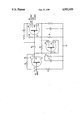
- the FIGURE is a circuit schematic of a first embodiment.
- FIG. 1 A schematic diagram of an MMIC FET amplifier according to the invention as described below is shown in the FIGURE A cascade of different size FETs is used.
- the size of the gate to source capacitance (“C gs ”) of the first stage FET 10 is chosen to provide a good input match.
- the size of the transconductance (“g m ”) of the second stage FET 20 is chosen to provide an acceptable gain. These choices dictate the size (or gate periphery) of these two devices.
- the first stage FET 10 consists of a gallium arsenide (“GaAs”) FET chosen to have a 250 micron gate length, providing about 3 dB of gain.
- GaAs gallium arsenide
- a shunt feedback loop connects the first stage drain output 12 to the first stage gate input 11 through a feedback resistor 14 connected in series with a DC block capacitor 15.
- Another resistor 19 is connected in parallel to the input in order to improve input VSWR beyond what is achievable with shunt feedback alone, and to ground this terminal.
- the first stage bias is then set by connecting the first stage source electrode 13 to a "self-bias" source resistor 16 which is bypassed by a capacitor 17 in order to float the DC ground and provide a short path to AC ground.
- the second stage FET 20 is chosen to be a 350 micron gate length GaAs FET, providing an additional 7 dB of gain.
- the second stage also has shunt feedback and self-biasing networks similar to the first stage.
- a resistive divider network, resistors 28 and 29, apply the correct bias voltage to the second stage gate electrode 21.
- a third GaAs FET 30, wired as a constant current source connects the second stage source terminal 23 to the first stage drain terminal 12.
- This constant current source serves to stabilize the bias currents of the RF FETs, making them less dependent on unavoidable process variations. It also exhibits the desirable property of suppressing the second harmonic content of the output waveform when the MMIC is operating in a large signal condition.
- a 500 ohm resistor 34 is connected in parallel to the current source to prevent the constant current source from taking most of the available voltage. This resistor is large enough with respect to the internal impedances to not affect the gain of the device significantly, yet small enough to help make the device less sensitive to variations in the pinchoff voltage.
- a DC blocking capacitor 35 is also required between the first and second stages to prevent the first stage drain voltage from becoming the second stage gate voltage.
Abstract
Description
Claims (10)
Priority Applications (1)
| Application Number | Priority Date | Filing Date | Title |
|---|---|---|---|
| US07/356,889 US4912430A (en) | 1989-05-24 | 1989-05-24 | Current source as a microwave biasing element |
Applications Claiming Priority (1)
| Application Number | Priority Date | Filing Date | Title |
|---|---|---|---|
| US07/356,889 US4912430A (en) | 1989-05-24 | 1989-05-24 | Current source as a microwave biasing element |
Publications (1)
| Publication Number | Publication Date |
|---|---|
| US4912430A true US4912430A (en) | 1990-03-27 |
Family
ID=23403383
Family Applications (1)
| Application Number | Title | Priority Date | Filing Date |
|---|---|---|---|
| US07/356,889 Expired - Lifetime US4912430A (en) | 1989-05-24 | 1989-05-24 | Current source as a microwave biasing element |
Country Status (1)
| Country | Link |
|---|---|
| US (1) | US4912430A (en) |
Cited By (10)
| Publication number | Priority date | Publication date | Assignee | Title |
|---|---|---|---|---|
| US5050235A (en) * | 1989-01-26 | 1991-09-17 | Nec Corporation | Transmitter using gallium arsenide FET with means for controlling gate bias voltage of the FET for suppressing undesired signal at a start condition of the transmitter |
| EP0544387A1 (en) * | 1991-10-29 | 1993-06-02 | STMicroelectronics, Inc. | High gain monolithic microwave integrated circuit amplifier |
| EP0601478A1 (en) * | 1992-12-04 | 1994-06-15 | Alcatel SEL Aktiengesellschaft | Cascaded transistor amplifier |
| US5387880A (en) * | 1993-10-20 | 1995-02-07 | Trw Inc. | Compact monolithic wide band HEMT low noise amplifiers with regulated self-bias |
| EP0703661A3 (en) * | 1994-09-23 | 1997-05-02 | At & T Corp | An apparatus for biasing a fet with a single voltage supply |
| US5808515A (en) * | 1996-01-18 | 1998-09-15 | Fujitsu Limited | Semiconductor amplifying circuit having improved bias circuit for supplying a bias voltage to an amplifying FET |
| US6294959B1 (en) * | 1999-11-12 | 2001-09-25 | Macmillan Bruce E. | Circuit that operates in a manner substantially complementary to an amplifying device included therein and apparatus incorporating same |
| US6545541B2 (en) * | 2001-05-29 | 2003-04-08 | Ericsson Inc. | Power amplifier embedded cell bias detection, methods of detecting bias in power amplifiers and systems utilizing embedded cell bias detection |
| KR100413399B1 (en) * | 1997-07-28 | 2004-03-22 | 지멘스 악티엔게젤샤프트 | Transistor amplifier stage |
| US20210273664A1 (en) * | 2020-02-27 | 2021-09-02 | STMicroelectronics (Alps) SAS | Device for generating radiofrequency signals in phase quadrature |
Citations (10)
| Publication number | Priority date | Publication date | Assignee | Title |
|---|---|---|---|---|
| GB369578A (en) * | 1930-12-20 | 1932-03-21 | William Beveridge Mackenzie | Improvements in and relating to electrical circuit arrangements using a gas discharge device, applicable to direct current amplifiers, and other electrical control amplifying and relaying apparatus |
| US3359503A (en) * | 1965-05-18 | 1967-12-19 | Motorola Inc | High gain amplifier employing cascaded opposite conductivity field effect transistors |
| US4004164A (en) * | 1975-12-18 | 1977-01-18 | International Business Machines Corporation | Compensating current source |
| US4390851A (en) * | 1980-11-25 | 1983-06-28 | Rockwell International Corporation | Monolithic microwave amplifier having active impedance matching |
| US4500848A (en) * | 1981-08-25 | 1985-02-19 | Lmt Radio Professionnelle | Field effect transistor microwave amplifier |
| US4612514A (en) * | 1983-04-08 | 1986-09-16 | Fujitsu Limited | Feedback amplifier |
| US4661789A (en) * | 1985-07-17 | 1987-04-28 | The United States Of America As Represented By The Secretary Of The Navy | Microwave recursive filter |
| US4686387A (en) * | 1984-01-20 | 1987-08-11 | Thomson-Csf | Biasing circuit for a field effect transistor |
| US4749959A (en) * | 1986-11-24 | 1988-06-07 | Celeritek, Inc. | Multiple FET device having direct-coupled stages for improved microwave operation |
| US4771247A (en) * | 1987-09-24 | 1988-09-13 | General Electric Company | MMIC (monolithic microwave integrated circuit) low noise amplifier |
-
1989
- 1989-05-24 US US07/356,889 patent/US4912430A/en not_active Expired - Lifetime
Patent Citations (10)
| Publication number | Priority date | Publication date | Assignee | Title |
|---|---|---|---|---|
| GB369578A (en) * | 1930-12-20 | 1932-03-21 | William Beveridge Mackenzie | Improvements in and relating to electrical circuit arrangements using a gas discharge device, applicable to direct current amplifiers, and other electrical control amplifying and relaying apparatus |
| US3359503A (en) * | 1965-05-18 | 1967-12-19 | Motorola Inc | High gain amplifier employing cascaded opposite conductivity field effect transistors |
| US4004164A (en) * | 1975-12-18 | 1977-01-18 | International Business Machines Corporation | Compensating current source |
| US4390851A (en) * | 1980-11-25 | 1983-06-28 | Rockwell International Corporation | Monolithic microwave amplifier having active impedance matching |
| US4500848A (en) * | 1981-08-25 | 1985-02-19 | Lmt Radio Professionnelle | Field effect transistor microwave amplifier |
| US4612514A (en) * | 1983-04-08 | 1986-09-16 | Fujitsu Limited | Feedback amplifier |
| US4686387A (en) * | 1984-01-20 | 1987-08-11 | Thomson-Csf | Biasing circuit for a field effect transistor |
| US4661789A (en) * | 1985-07-17 | 1987-04-28 | The United States Of America As Represented By The Secretary Of The Navy | Microwave recursive filter |
| US4749959A (en) * | 1986-11-24 | 1988-06-07 | Celeritek, Inc. | Multiple FET device having direct-coupled stages for improved microwave operation |
| US4771247A (en) * | 1987-09-24 | 1988-09-13 | General Electric Company | MMIC (monolithic microwave integrated circuit) low noise amplifier |
Cited By (11)
| Publication number | Priority date | Publication date | Assignee | Title |
|---|---|---|---|---|
| US5050235A (en) * | 1989-01-26 | 1991-09-17 | Nec Corporation | Transmitter using gallium arsenide FET with means for controlling gate bias voltage of the FET for suppressing undesired signal at a start condition of the transmitter |
| EP0544387A1 (en) * | 1991-10-29 | 1993-06-02 | STMicroelectronics, Inc. | High gain monolithic microwave integrated circuit amplifier |
| EP0601478A1 (en) * | 1992-12-04 | 1994-06-15 | Alcatel SEL Aktiengesellschaft | Cascaded transistor amplifier |
| US5387880A (en) * | 1993-10-20 | 1995-02-07 | Trw Inc. | Compact monolithic wide band HEMT low noise amplifiers with regulated self-bias |
| EP0703661A3 (en) * | 1994-09-23 | 1997-05-02 | At & T Corp | An apparatus for biasing a fet with a single voltage supply |
| US5808515A (en) * | 1996-01-18 | 1998-09-15 | Fujitsu Limited | Semiconductor amplifying circuit having improved bias circuit for supplying a bias voltage to an amplifying FET |
| KR100413399B1 (en) * | 1997-07-28 | 2004-03-22 | 지멘스 악티엔게젤샤프트 | Transistor amplifier stage |
| US6294959B1 (en) * | 1999-11-12 | 2001-09-25 | Macmillan Bruce E. | Circuit that operates in a manner substantially complementary to an amplifying device included therein and apparatus incorporating same |
| US6545541B2 (en) * | 2001-05-29 | 2003-04-08 | Ericsson Inc. | Power amplifier embedded cell bias detection, methods of detecting bias in power amplifiers and systems utilizing embedded cell bias detection |
| US20210273664A1 (en) * | 2020-02-27 | 2021-09-02 | STMicroelectronics (Alps) SAS | Device for generating radiofrequency signals in phase quadrature |
| US11757477B2 (en) * | 2020-02-27 | 2023-09-12 | STMicroelectronics (Alps) SAS | Device for generating radiofrequency signals in phase quadrature |
Similar Documents
| Publication | Publication Date | Title |
|---|---|---|
| US5486787A (en) | Monolithic microwave integrated circuit apparatus | |
| US5365197A (en) | Low-noise distributed amplifier | |
| US4788511A (en) | Distributed power amplifier | |
| JP3901780B2 (en) | High frequency amplifier | |
| US6137367A (en) | High power high impedance microwave devices for power applications | |
| US6750711B2 (en) | RF power amplifier stability | |
| US5408198A (en) | Semiconductor power amplifier integrated circuit | |
| US6472941B2 (en) | Distributed amplifier with terminating circuit capable of improving gain flatness at low frequencies | |
| JPH022702A (en) | Variable attenuator | |
| US5694085A (en) | High-power amplifier using parallel transistors | |
| US4912430A (en) | Current source as a microwave biasing element | |
| US4864250A (en) | Distributed amplifier having improved D.C. biasing and voltage standing wave ratio performance | |
| US4841253A (en) | Multiple spiral inductors for DC biasing of an amplifier | |
| US4760350A (en) | Internally matched power amplifier | |
| US20030048138A1 (en) | High frequency power amplifier circuit | |
| US4908531A (en) | Monolithic active isolator | |
| US3991381A (en) | Linear high power transistor amplifier | |
| EP0355670B1 (en) | Low noise microwave amplifier having optimal stability, gain, and noise control | |
| US6400222B1 (en) | Linearizer | |
| US5017887A (en) | High frequency IC power amplifier | |
| US5338989A (en) | Microwave integrated circuit | |
| US4853564A (en) | GaAs monolithic true logarithmic amplifier | |
| JP3589437B2 (en) | Power amplifier | |
| JPS6318889B2 (en) | ||
| JPH04287507A (en) | Field effect transistor amplifier |
Legal Events
| Date | Code | Title | Description |
|---|---|---|---|
| AS | Assignment |
Owner name: AVANTEK, INC., 481 COTTONWOOD DRIVE, MILPITAS, CA Free format text: ASSIGNMENT OF ASSIGNORS INTEREST.;ASSIGNOR:FRANK, MICHAEL L.;REEL/FRAME:005085/0771 Effective date: 19890518 |
|
| STCF | Information on status: patent grant |
Free format text: PATENTED CASE |
|
| FEPP | Fee payment procedure |
Free format text: PAYOR NUMBER ASSIGNED (ORIGINAL EVENT CODE: ASPN); ENTITY STATUS OF PATENT OWNER: LARGE ENTITY |
|
| FPAY | Fee payment |
Year of fee payment: 4 |
|
| AS | Assignment |
Owner name: HEWLETT-PACKARD COMPANY, CALIFORNIA Free format text: ASSIGNMENT OF ASSIGNORS INTEREST;ASSIGNOR:AVANTEK, INC.;REEL/FRAME:007185/0155 Effective date: 19941026 |
|
| FPAY | Fee payment |
Year of fee payment: 8 |
|
| AS | Assignment |
Owner name: HEWLETT-PACKARD COMPANY, A DELAWARE CORPORATION, C Free format text: MERGER;ASSIGNOR:HEWLETT-PACKARD COMPANY, A CALIFORNIA CORPORATION;REEL/FRAME:010841/0649 Effective date: 19980520 |
|
| AS | Assignment |
Owner name: AGILENT TECHNOLOGIES INC., CALIFORNIA Free format text: ASSIGNMENT OF ASSIGNORS INTEREST;ASSIGNOR:HEWLETT-PACKARD COMPANY, A DELAWARE CORPORATION;REEL/FRAME:010901/0336 Effective date: 20000520 |
|
| FPAY | Fee payment |
Year of fee payment: 12 |
|
| AS | Assignment |
Owner name: AVAGO TECHNOLOGIES GENERAL IP PTE. LTD., SINGAPORE Free format text: ASSIGNMENT OF ASSIGNORS INTEREST;ASSIGNOR:AGILENT TECHNOLOGIES, INC.;REEL/FRAME:017207/0020 Effective date: 20051201 |
|
| AS | Assignment |
Owner name: CITICORP NORTH AMERICA, INC.,DELAWARE Free format text: SECURITY AGREEMENT;ASSIGNOR:AVAGO TECHNOLOGIES GENERAL IP (SINGAPORE) PTE. LTD.;REEL/FRAME:017207/0882 Effective date: 20051201 Owner name: CITICORP NORTH AMERICA, INC., DELAWARE Free format text: SECURITY AGREEMENT;ASSIGNOR:AVAGO TECHNOLOGIES GENERAL IP (SINGAPORE) PTE. LTD.;REEL/FRAME:017207/0882 Effective date: 20051201 |
|
| AS | Assignment |
Owner name: AVAGO TECHNOLOGIES WIRELESS IP (SINGAPORE) PTE. LT Free format text: ASSIGNMENT OF ASSIGNORS INTEREST;ASSIGNOR:AVAGO TECHNOLOGIES GENERAL IP (SINGAPORE) PTE. LTD;REEL/FRAME:017675/0434 Effective date: 20060127 |
|
| AS | Assignment |
Owner name: AVAGO TECHNOLOGIES GENERAL IP (SINGAPORE) PTE. LTD Free format text: CORRECTIVE ASSIGNMENT TO CORRECT THE NAME OF THE ASSIGNEE PREVIOUSLY RECORDED ON REEL 017207 FRAME 0020. ASSIGNOR(S) HEREBY CONFIRMS THE ASSIGNMENT;ASSIGNOR:AGILENT TECHNOLOGIES, INC.;REEL/FRAME:038633/0001 Effective date: 20051201 |