US4947225A - Sub-micron devices with method for forming sub-micron contacts - Google Patents
Sub-micron devices with method for forming sub-micron contacts Download PDFInfo
- Publication number
- US4947225A US4947225A US07/073,591 US7359187A US4947225A US 4947225 A US4947225 A US 4947225A US 7359187 A US7359187 A US 7359187A US 4947225 A US4947225 A US 4947225A
- Authority
- US
- United States
- Prior art keywords
- micron
- active region
- electrodes
- tops
- collector
- Prior art date
- Legal status (The legal status is an assumption and is not a legal conclusion. Google has not performed a legal analysis and makes no representation as to the accuracy of the status listed.)
- Expired - Lifetime
Links
- 238000000034 method Methods 0.000 title abstract description 30
- 229910021420 polycrystalline silicon Inorganic materials 0.000 claims abstract description 84
- 229920005591 polysilicon Polymers 0.000 claims abstract description 84
- 229910052751 metal Inorganic materials 0.000 claims description 31
- 239000002184 metal Substances 0.000 claims description 31
- 238000009413 insulation Methods 0.000 claims description 15
- 239000000758 substrate Substances 0.000 claims description 13
- 238000009792 diffusion process Methods 0.000 claims description 9
- 239000011521 glass Substances 0.000 claims description 8
- 239000004020 conductor Substances 0.000 claims description 6
- 150000004767 nitrides Chemical class 0.000 abstract description 60
- 230000008569 process Effects 0.000 abstract description 15
- 230000003647 oxidation Effects 0.000 abstract description 12
- 238000007254 oxidation reaction Methods 0.000 abstract description 12
- 238000004519 manufacturing process Methods 0.000 abstract description 11
- 239000010410 layer Substances 0.000 description 54
- 229920002120 photoresistant polymer Polymers 0.000 description 22
- 239000007943 implant Substances 0.000 description 13
- 238000005530 etching Methods 0.000 description 7
- 229910052698 phosphorus Inorganic materials 0.000 description 7
- 229910052796 boron Inorganic materials 0.000 description 6
- 150000002500 ions Chemical class 0.000 description 6
- 239000011574 phosphorus Substances 0.000 description 6
- XUIMIQQOPSSXEZ-UHFFFAOYSA-N Silicon Chemical compound [Si] XUIMIQQOPSSXEZ-UHFFFAOYSA-N 0.000 description 5
- -1 boron ions Chemical class 0.000 description 5
- 229910052710 silicon Inorganic materials 0.000 description 5
- 239000010703 silicon Substances 0.000 description 5
- OAICVXFJPJFONN-UHFFFAOYSA-N Phosphorus Chemical compound [P] OAICVXFJPJFONN-UHFFFAOYSA-N 0.000 description 4
- ZOXJGFHDIHLPTG-UHFFFAOYSA-N Boron Chemical compound [B] ZOXJGFHDIHLPTG-UHFFFAOYSA-N 0.000 description 3
- 229910001218 Gallium arsenide Inorganic materials 0.000 description 3
- 238000005516 engineering process Methods 0.000 description 3
- IJGRMHOSHXDMSA-UHFFFAOYSA-N Atomic nitrogen Chemical compound N#N IJGRMHOSHXDMSA-UHFFFAOYSA-N 0.000 description 2
- 239000002019 doping agent Substances 0.000 description 2
- 238000002955 isolation Methods 0.000 description 2
- 230000000873 masking effect Effects 0.000 description 2
- 239000000463 material Substances 0.000 description 2
- 229910052757 nitrogen Inorganic materials 0.000 description 2
- 230000001590 oxidative effect Effects 0.000 description 2
- 238000001020 plasma etching Methods 0.000 description 2
- 238000012421 spiking Methods 0.000 description 2
- OQCFWECOQNPQCG-UHFFFAOYSA-N 1,3,4,8-tetrahydropyrimido[4,5-c]oxazin-7-one Chemical compound C1CONC2=C1C=NC(=O)N2 OQCFWECOQNPQCG-UHFFFAOYSA-N 0.000 description 1
- 229910052581 Si3N4 Inorganic materials 0.000 description 1
- VYPSYNLAJGMNEJ-UHFFFAOYSA-N Silicium dioxide Chemical compound O=[Si]=O VYPSYNLAJGMNEJ-UHFFFAOYSA-N 0.000 description 1
- NRTOMJZYCJJWKI-UHFFFAOYSA-N Titanium nitride Chemical compound [Ti]#N NRTOMJZYCJJWKI-UHFFFAOYSA-N 0.000 description 1
- 238000001015 X-ray lithography Methods 0.000 description 1
- 230000003213 activating effect Effects 0.000 description 1
- 230000004913 activation Effects 0.000 description 1
- CSDREXVUYHZDNP-UHFFFAOYSA-N alumanylidynesilicon Chemical compound [Al].[Si] CSDREXVUYHZDNP-UHFFFAOYSA-N 0.000 description 1
- 230000004888 barrier function Effects 0.000 description 1
- 150000001875 compounds Chemical class 0.000 description 1
- 230000006378 damage Effects 0.000 description 1
- 230000000694 effects Effects 0.000 description 1
- 238000000609 electron-beam lithography Methods 0.000 description 1
- 239000012467 final product Substances 0.000 description 1
- 230000001939 inductive effect Effects 0.000 description 1
- 230000010354 integration Effects 0.000 description 1
- 238000005468 ion implantation Methods 0.000 description 1
- 238000001465 metallisation Methods 0.000 description 1
- 239000012299 nitrogen atmosphere Substances 0.000 description 1
- 238000012856 packing Methods 0.000 description 1
- 239000000047 product Substances 0.000 description 1
- 230000004224 protection Effects 0.000 description 1
- 230000001681 protective effect Effects 0.000 description 1
- 230000005855 radiation Effects 0.000 description 1
- 230000000717 retained effect Effects 0.000 description 1
- 229910021332 silicide Inorganic materials 0.000 description 1
- HQVNEWCFYHHQES-UHFFFAOYSA-N silicon nitride Chemical compound N12[Si]34N5[Si]62N3[Si]51N64 HQVNEWCFYHHQES-UHFFFAOYSA-N 0.000 description 1
- 229910052814 silicon oxide Inorganic materials 0.000 description 1
- 239000002356 single layer Substances 0.000 description 1
- 238000005245 sintering Methods 0.000 description 1
- 239000007787 solid Substances 0.000 description 1
- 230000007704 transition Effects 0.000 description 1
- 239000002699 waste material Substances 0.000 description 1
Images


Classifications
-
- H—ELECTRICITY
- H01—ELECTRIC ELEMENTS
- H01L—SEMICONDUCTOR DEVICES NOT COVERED BY CLASS H10
- H01L29/00—Semiconductor devices adapted for rectifying, amplifying, oscillating or switching, or capacitors or resistors with at least one potential-jump barrier or surface barrier, e.g. PN junction depletion layer or carrier concentration layer; Details of semiconductor bodies or of electrodes thereof ; Multistep manufacturing processes therefor
- H01L29/66—Types of semiconductor device ; Multistep manufacturing processes therefor
- H01L29/66007—Multistep manufacturing processes
- H01L29/66075—Multistep manufacturing processes of devices having semiconductor bodies comprising group 14 or group 13/15 materials
- H01L29/66227—Multistep manufacturing processes of devices having semiconductor bodies comprising group 14 or group 13/15 materials the devices being controllable only by the electric current supplied or the electric potential applied, to an electrode which does not carry the current to be rectified, amplified or switched, e.g. three-terminal devices
- H01L29/66234—Bipolar junction transistors [BJT]
- H01L29/66272—Silicon vertical transistors
-
- H—ELECTRICITY
- H01—ELECTRIC ELEMENTS
- H01L—SEMICONDUCTOR DEVICES NOT COVERED BY CLASS H10
- H01L21/00—Processes or apparatus adapted for the manufacture or treatment of semiconductor or solid state devices or of parts thereof
- H01L21/02—Manufacture or treatment of semiconductor devices or of parts thereof
- H01L21/04—Manufacture or treatment of semiconductor devices or of parts thereof the devices having at least one potential-jump barrier or surface barrier, e.g. PN junction, depletion layer or carrier concentration layer
- H01L21/18—Manufacture or treatment of semiconductor devices or of parts thereof the devices having at least one potential-jump barrier or surface barrier, e.g. PN junction, depletion layer or carrier concentration layer the devices having semiconductor bodies comprising elements of Group IV of the Periodic System or AIIIBV compounds with or without impurities, e.g. doping materials
- H01L21/28—Manufacture of electrodes on semiconductor bodies using processes or apparatus not provided for in groups H01L21/20 - H01L21/268
- H01L21/283—Deposition of conductive or insulating materials for electrodes conducting electric current
- H01L21/285—Deposition of conductive or insulating materials for electrodes conducting electric current from a gas or vapour, e.g. condensation
- H01L21/28506—Deposition of conductive or insulating materials for electrodes conducting electric current from a gas or vapour, e.g. condensation of conductive layers
- H01L21/28512—Deposition of conductive or insulating materials for electrodes conducting electric current from a gas or vapour, e.g. condensation of conductive layers on semiconductor bodies comprising elements of Group IV of the Periodic System
- H01L21/28525—Deposition of conductive or insulating materials for electrodes conducting electric current from a gas or vapour, e.g. condensation of conductive layers on semiconductor bodies comprising elements of Group IV of the Periodic System the conductive layers comprising semiconducting material
-
- H—ELECTRICITY
- H01—ELECTRIC ELEMENTS
- H01L—SEMICONDUCTOR DEVICES NOT COVERED BY CLASS H10
- H01L29/00—Semiconductor devices adapted for rectifying, amplifying, oscillating or switching, or capacitors or resistors with at least one potential-jump barrier or surface barrier, e.g. PN junction depletion layer or carrier concentration layer; Details of semiconductor bodies or of electrodes thereof ; Multistep manufacturing processes therefor
- H01L29/66—Types of semiconductor device ; Multistep manufacturing processes therefor
- H01L29/68—Types of semiconductor device ; Multistep manufacturing processes therefor controllable by only the electric current supplied, or only the electric potential applied, to an electrode which does not carry the current to be rectified, amplified or switched
- H01L29/70—Bipolar devices
- H01L29/72—Transistor-type devices, i.e. able to continuously respond to applied control signals
- H01L29/73—Bipolar junction transistors
- H01L29/732—Vertical transistors
- H01L29/7322—Vertical transistors having emitter-base and base-collector junctions leaving at the same surface of the body, e.g. planar transistor
-
- H—ELECTRICITY
- H01—ELECTRIC ELEMENTS
- H01L—SEMICONDUCTOR DEVICES NOT COVERED BY CLASS H10
- H01L29/00—Semiconductor devices adapted for rectifying, amplifying, oscillating or switching, or capacitors or resistors with at least one potential-jump barrier or surface barrier, e.g. PN junction depletion layer or carrier concentration layer; Details of semiconductor bodies or of electrodes thereof ; Multistep manufacturing processes therefor
- H01L29/66—Types of semiconductor device ; Multistep manufacturing processes therefor
- H01L29/68—Types of semiconductor device ; Multistep manufacturing processes therefor controllable by only the electric current supplied, or only the electric potential applied, to an electrode which does not carry the current to be rectified, amplified or switched
- H01L29/70—Bipolar devices
- H01L29/72—Transistor-type devices, i.e. able to continuously respond to applied control signals
- H01L29/73—Bipolar junction transistors
- H01L29/735—Lateral transistors
-
- H—ELECTRICITY
- H01—ELECTRIC ELEMENTS
- H01L—SEMICONDUCTOR DEVICES NOT COVERED BY CLASS H10
- H01L29/00—Semiconductor devices adapted for rectifying, amplifying, oscillating or switching, or capacitors or resistors with at least one potential-jump barrier or surface barrier, e.g. PN junction depletion layer or carrier concentration layer; Details of semiconductor bodies or of electrodes thereof ; Multistep manufacturing processes therefor
- H01L29/66—Types of semiconductor device ; Multistep manufacturing processes therefor
- H01L29/68—Types of semiconductor device ; Multistep manufacturing processes therefor controllable by only the electric current supplied, or only the electric potential applied, to an electrode which does not carry the current to be rectified, amplified or switched
- H01L29/76—Unipolar devices, e.g. field effect transistors
- H01L29/772—Field effect transistors
- H01L29/78—Field effect transistors with field effect produced by an insulated gate
Definitions
- the invention provides sub-micron VLSI devices with contacts of the order of 0.9 down to 0.1 microns.
- a severe limitation for large scale integration is the lack of adequate registration from layer to layer during the fabrication process. These mis-registrations result in the introduction of guards/protections which enlarge the real estate area needed for a particular circuit layout.
- the invention can be applied to MOS (n-, p-, CMOS), Bipolar, or GaAs devices.
- MOS n-, p-, CMOS
- Bipolar Bipolar
- GaAs GaAs
- an oversized contact mask is applied and the insulating layer (oxide) etched so as to expose the substrate material or that to be accessed.
- a layer of undoped polysilicon is deposited; here, the thickness of this polysilicon layer must be selected according to the desired size of the contact to be fabricated, and planarization of the insulation desired. For instance, for a contact size of 0.1 by 0.1 microns, the layer of polysilicon can be approximately 1000 angstroms.
- a thin layer of silicon nitride is deposited on top of the polysilicon.
- nitride contact buttons are delineated with photoresist.
- the underlying layer of unprotected nitride is selectively etched, the photoresist is removed and the exposed polysilicon is oxidized.
- the nitride buttons protect the polysilicon underneath, hence preventing oxidation.
- the nitride is selectively removed from the contact areas.
- the proper doping is performed by ion implantation and photoresist masking steps.
- a layer of metal is deposited over the entire wafer, patterned with the aid of a metallization mask over a photoresist layer; the metal is etched and the photoresist is removed.
- the devices are sintered to complete the fabrication process alternatively, in lieu of oxidizing the polysilicon, the poly contact shiskers may be covered with low temperature oxide, followed by a layer of SOG. The tops of the poly whiskers are uncovered for doping of the contacts, as above.
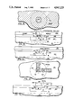
- FIG. 1 is a view of the active region mask relative to a wafer with a layer of oxide and nitride as a conventional step in surrounding the active region with field oxide;
- FIG. 1A shows the removal of the oxide and nitride from the regions other than the active areas
- FIG. 1B shows the nitride layer to be used as the mask during oxidation
- FIG. lC shows the field oxide grown
- FIG. lD shows the layer of polysilicon over the oxidized wafer and field oxide
- FIG. 2 shows the polysilicon delineated for the gate
- FIG. 3 shows source and drain activation by phosphorus implant
- FIG. 4A shows a contact mask
- FIG. 4 shows the structure after extra large contact apertures have been opened to the bare silicon
- FIG. 5 is an overview of the opened contact openings in the structure as seen in top plan view
- FIG. 6 is a mask for developing nitride buttons over the contact regions
- FIG. 7 shows the resist being retained in the three contact areas over the nitride layer
- FIG. 8 shows the nitride removed except where it was covered by the resist and the polysilicon converted to polyoxide except in the electrode regions protected by the nitride buttons;
- FIG. 9 is a view in plan of the interconnects and contact regions
- FIG. 10 shows the completed device with the sub-micron contacts
- FIG. 11 is a view in top plan of a conventional bipolar device constructed to the stage of FIGS. 11 and 12 by conventional means;
- FIG. 12 is a view in cross-section of the bipolar device
- FIG. 13 shows the steps for commencing the fabrication of the small contacts by employing a layer of polysilicon covered by a layer of nitride
- FIG. 14 shows the device of FIG. 13 in top plan view
- FIG. 14A is a mask for retaining resist over nitride button areas for contacts to the collector and base regions;
- FIG. 15 shows the nitride buttons protected by the resist with the nitride layer otherwise removed and a portion of the polyoxide removed, the polysilicon having been converted to polyoxide where uncovered by the nitride removal;
- FIG. 16 shows the mask for opening the contact region for the base
- FIG. 17 shows the ion implanting of boron ions through this opening into the base contact region to dope the polysilicon base electrode
- FIG. 18 shows the mask for opening the contact region over the collector electrodes
- FIG. 19 shows this region opened and phosphorus implant taking place to dope the polysilicon collector electrode
- FIG. 20 shows a layer of metal applied over these two electrodes
- FIG. 21 shows a metal contact mask
- FIG. 22 shows the completed device with the metal interconnects for the two contacts
- FIG. 23 is a view in top plan of a bipolar device of the Soclof type
- FIG. 24 shows the device of FIG. 23 in cross-section in field oxide
- FIG. 25 shows the application of a polysilicon layer covered by a nitride layer to the structure of FIG. 24;
- FIG. 26 shows a contact mask
- FIG. 27 shows the nitride buttons remaining over each of the bipolar elements atop the polysilicon layer
- FIG. 28 shows the polysilicon layer converted to polyoxide except where the nitride buttons preserve the polysilicon
- FIG. 29 shows the structure after removal of the nitride buttons
- FIG. 30 shows the mask for activating the base electrode polysilicon
- FIG. 31 shows the boron implant to achieve the doping of the polysilicon electrode
- FIG. 32 shows a mask for opening regions to the collector and emitter (N regions);
- FIG. 33 shows these regions opened and the polysilicon therein being doped by phosphorus implant
- FIG. 34 shows the nitride buttons removed and the layer of metal over top of the structure
- FIG. 35 shows the arrangement in top plan view as delineated by the mask of FIG. 36;
- FIG. 37 shows the completed device following sintering
- FIG. 38 shows dimensions achievable in the contact regions for these devices
- FIG. 39 shows the NPN elements of a transistor being formed embedded in oxide and covered by a layer of polysilicon, in turn covered by a layer of nitride;
- FIG. 40 is a contact mask
- FIG. 41 shows the nitride contact buttons
- FIG. 42 depicts the isolated polysilicon contacts
- FIG. 43 reveals the plasma oxide covering the contacts, and in turn covered by glass (SOG);
- FIG. 44 planarizes the structure of FIG. 43 down to the tops of the nitride buttons
- FIG. 45 shows the structure of FIG. 44 with the nitride buttons removed
- FIG. 46 shows the mask to be used in making a doping opening to the base contact
- FIG. 47 shows the doping step for the base contact
- FIG. 47A shows a mask for making openings to the collector and emitter contacts
- FIG. 48 shows the doping step for the collector and emitter contacts
- FIG. 49 includes the metal interconnect layer
- FIG. 50 shows the delineated metal interconnects
- FIG. 51 shows the mask for effecting the delineation
- FIG. 52 shows the completed device
- FIG. 53 is an example of relative sizes available from this method.
- FIGS. 1 through FIG. 2 are conventional steps leading to the structure of FIG. 2 wherein processing is directed to the fabrication of the sub-micron contacts.
- P doped silicon wafer 10 is first thermally oxidized to produce the silicon oxide layer 11, followed by a deposit of nitride layer 12, and the use of active region mask 13 to delineate photoresist 14 over the nitride layer 12.
- the resist 14 permits etching away of the nitride layer 12 and oxide layer 11 everywhere except in the protected active region in order to provide for the field implant, shown as the boron ions implanted into the wafer 10 everywhere except in the active regions, as best seen in FIG. lA.
- a 70 Kev implant is used at a dose of ⁇ 10 12 ions/cm 2 .
- FIG. lB the resist 14 has been removed and the ion implant is illustrated at 15'.
- the field oxide 16 is grown using the nitride layer 12 to prevent oxidation in the active region.
- nitride layer 12 and oxide 11 are stripped, followed by growing gate oxide 20 in FIG. lD.
- FIG. lD a layer of deposited polysilicon 21 is shown over the gate oxide 20.
- FIG. 2 shows the structure after employing a gate mask to delineate the polysilicon 21 relative to the active region 22.
- the polysilicon 21 forms the gate electrode 23.
- the first step of growing a thin oxide layer 25 of approximately 200 to 600 angstroms thick is pursued toward delineating the contacts.
- FIGS. 4 and 4A show the wafer 10 opened to bare silicon by contact mask 50.
- Photoresist 51 is applied over the structure of FIG. 3 and mask 50 is used to open both the photoresist 51 and the oxide 20 in the source and drain region. These contact regions are made extra large in order that registration errors may be minimized in arriving at the final product.
- the opening 53 in mask 50 is illustrated in FIG. 5 for the gate contact region 53, source opening 55 being designated by the left opening in contact mask 50 and drain opening designated by the right aperture 57.
- an N+ doped polysilicon layer 58 is deposited on the previous structure to a thickness of approximately 2000 angstroms for fabricating contacts of the order of 0.1 microns by 0.1 microns (thinner polysilicon can be used for even smaller contacts).
- 5000 angstroms of polysilicon may be used for contacts over 3 microns, 3000 angstroms for contacts of 1 1/2microns and 1000 microns for contacts of the order of 0.1-0.2 microns.
- these figures may require slight adjustment, but they may be extrapolated and successfully used for an initial run.
- the polysilicon thickness is simply doubled, (i.e.) 1000 angstroms becomes 2000 angstroms.
- the next step is to deposit nitride 60 to a depth of about 1000 angstroms.
- the contact mask 61 of FIG. 6 is employed to delineate the protective resist 62 over the source, resist 63 over the gate, and resist 64 over the drain.
- the next step is to etch the nitride layer 60 and approximately one half of the polysilicon while the three regions are protected by the photoresist. This is achieved by employing an anisotropic etch conventionally to remove one half of the polysilicon and all of the unprotected nitride, the buttons being protected by the resist. Then, the resist is stripped and the unprotected polysilicon 58 is oxidized to become oxide 58'. Nitride buttons 60A, 60B and 60C cover the unoxidized polysilicon 58 over the source, gate, and drain.
- FIGS. 9 and 10 show the finished NMOS device.
- the nitride buttons 60A, 60B and 60C are stripped thereby leaving the polysilicon 58A source electrode, polysilicon 58B gate electrode and polysilicon 58C drain electrode in the polyoxide 58'.
- the next step is to deposit aluminum silicon followed, by masking the metal to delineate the source conductor or interconnect 70, gate interconnect 71 and drain interconnect 72.
- the minimum overlap of active region (active mask 13, FIG. 1 and contact regions, FIG. 5) relative to contact (electrode areas 58) had to be at least 0.8 microns.
- the electrodes 58 are doped with the same material as the source and drain junctions (N+) being connected, there is no possibility for the metal interconnect to short circuit from junction to substrate, as is the problem with the prior art resulting in the requirements for large area overlap.
- the electrodes being polysilicon, prevent the metal from spiking through shallow junctions (i.e.) sub-micron type junctions.
- the contacts are of the order of 0.1 microns because:
- FIG's. 6 and 7 significant steps are illustrated for making the sub-micron contacts. It is necessary that the polysilicon 58 make contact with the already formed sources and drains because the delineated electrodes 58A and 58C are polysilicon which is covered by the nitride buttons 60A and 60C. The dimensions of these electrodes is established by the solid regions of mask 61. The masks are used for larger sizes. For smaller sizes, the E-Beam is blanked out for these regions when making contacts down to 0.1 by 0.1 microns under computer control. Many current E-Beam micro-fabricators have spot sizes down to 0.1 microns, or less.
- the present invention improves over the patent by a technique which eliminates "sidewalk” effects by creating a flat field, thus, eliminating the "111 " transition region from active to field regions. Also, overlap of gate electrode over field regions is totally eliminated by routing gate electrode metal interconnect by running it over the source or drain, thus inducing radiation hardness. This is particularly desirable in sub-micron devices for general use by the military, and in commercial space applications.
- FIGS. 11 and 12 illustrate a conventional bipolar transistor structure wherein the wafer 101 is doped N+ and the emitter 103 is defined and diffused with n-type dopant, the base 105 is similarly defined and diffused with p-type dopant and the collector 107 is doped n-type.
- This basic structure can be produced by any of the conventional processing techniques to this stage ready to receive the sub-micron contacts through processing steps described hereinafter.
- a layer of undoped polysilicon 110 is deposited over wafer 101 with a layer of nitride 112 deposited over the polysilicon layer 110.
- the thickness of the polysilicon layer 110 is preferably 2000 angstroms (for 0.1 micron contacts) approximately and the thickness of the nitride layer 112 is approximately 1000 angstroms.
- the next step is to mask the contact regions using contact mask 115 of FIG. 14A to retain photoresist 117 over nitride buttons 112' and 112'' for the emitter 103 contact and the base 105 contact.
- This permits anisotropic etching to be carried on conventionally to remove approximately one half of the polysilicon thickness and all of the nitride, except where protected by photoresist 117, i.e., the buttons.
- the polysilicon 110 is oxidized into polyoxide 110'. It should be noted that approximately half or 1000 angstroms of the polysilicon 110 was etched away, along with the nitride 112, such that when the polysilicon is oxidized into polyoxide 110', the level of the top is approximately coplanar to the original level of the top of the polysilicon 110. However, at the start of oxidation, the thickness of the polysilicon was 1000 angstroms to produce 0.1 micron contacts.
- nitride contact buttons 112' and 112'' are etched away because they have served their purpose of protecting the polysilicon electrode regions 121 and 123 for the emitter 103 and base 105 from oxidation when the polysilicon layer 110 was converted to polyoxide 110'.
- the next step is to mask the P contact region by employing mask 125' with opening, 126 as shown in FIG. 16.
- the photoresist 127 is opened in the aperture 127' and boron ions are implanted, as shown by the arrows 131 using a 60 Kev implanter with a dose of 1 to 5 ⁇ 10 15 ions per cm 2 .
- the resist 127 is stripped and the mask of FIG. 18 is employed in similar manner to implant phosphorus ions, shown by the arrows 131 into the N contact region represented by the aperture 132 produced by the aperture 133 in mask 134 of FIG. 18.
- a dose of 1 to 5 ⁇ 10 15 ions per square centimeter is preferred.
- the resist 135 is stripped and the implants are annealed at 8OO° C. for 40 minutes in nitrogen.
- FIG. 22 represents this layer of metal which is covered with photoresist and exposed through the mask 151 for etching to leave the emitter contact 155 and base contact 157 on the polyoxide layer 110' and in contact with the emitter electrode 121 and the base electrode 123, respectively.
- the device is sintered for a completed product.
- the actual contact regions are shown by the squares marked 121' and 123', visible in the mask 151. These contact regions may be of the order of 0.1 by 0.1 microns per contact.
- FIG. 23 a plan view of a Soclof bipolar transistor is shown, as described in U.S. Pat. Nos.
- the collector, base, and emitter 201, 202 and 203 comprise substantially the transistor, there being field oxide 204 about each device.
- the collector is shown as being N doped, the base P doped, and the emitter N doped.
- the bipolar transistors may be manufactured to the stage shown in FIG. 24, in accordance with the process of any one of the Soclof patents.
- the first step in building sub-micron contacts for these devices is to deposit undoped polysilicon to approximately 2000 angstroms. This layer is shown at 205 and, again, if the contacts are to be larger more polysilicon can be used.
- a layer 206 of nitride is deposited to a thickness of approximately 1000 angstroms, as thus shown in FIG. 25.
- the mask 207 of FIG. 26 is employed with photoresist (not shown) to delineate the nitride 206, thereby leaving the nitride buttons 211, 212 and 213 over the collector 201, base 202 and emitter 203 respectively.
- nitride a portion of the polysilicon is also removed. This may comprise one half of the polysilicon so that 1000 angstroms of polysilicon is really used for 0.1 micron contacts.
- the nitride and polysilicon are removed by anisotropic etch over a predetermined conventional time period.
- the resist is stripped and the polysilicon oxidized to become polyoxide 221, shown in FIG. 28.
- the polyoxide 221 also fills in the spaces between the nitride buttons 211, 212 and 213 to insulate the contacts from each other.
- FIG. 29 shows the structure after the nitride buttons 211, 212 and 213 have been removed by etching or stripping.
- mask 250 is used, together with photoresist 251 to open aperture 253 into the P doped base 202.
- implanting is carried out using a 60 Kev implanter with a 1 to 5 ⁇ 10 15 ions per cm 2 dose.
- the photoresist 251 is stripped and a new layer applied for use with the mask 270 to open the new layer of photoresist 271 above the collector 201, and emitter 203.
- the phosphorus ions are implanted, the photoresist 271 is stripped and the device of FIG. 33 is annealed for the implants at 800° C. for 40 minutes in a nitrogen atmosphere.
- a metal layer 300 has been applied over the structure, photoresist and the mask are applied and the metal is etched to provide a metal interconnect 311 (FIG. 35) to the collector 201, interconnect 312 to the base 202 and interconnect 313 to the emitter 203.
- FIG. 38 shows relative sizes for the bipolar device, the elements themselves, such as the collector measuring 0.3 by 0.3 microns and the contact regions measuring 0.1 by 0.1 microns.
- the contacts can be oversized to approximately 0.3 microns and the elements may measure 0.9 ⁇ 0.9 microns.
- the principles disclosed permit 3 and 4 micron devices with (e.g.) 0.9 ⁇ 1.0 plus micron contacts if desired.
- single MOS or bipolar devices may be made, and it is only necessary to insulate them by isolation, usually in lieu of the field oxide, illustrated.
- the present invention provides the most minimal size Soclof type (totally lateral) bipolar devices attainable because they consist primarily of active elements.
- Soclof type totally lateral bipolar devices attainable because they consist primarily of active elements.
- minimal size contacts are also obtained down to 0.1 ⁇ 0.1 microns, or to 0.1 micron diameter where the spot size is 0.1 micron or less.
- FIG. 39 Yet another alternative method for forming the 0.1 to 0.9 micron contacts is disclosed, beginning with FIG. 39 wherein the three elements, collector 201', base 202' and emitter 203' are first covered by polysilicon 205' to a depth of, e.g., approximately 3000 angstroms, and nitride 325 is deposited to a depth of, e.g., approximately 1000 angstroms.
- Mask 327 (FIG. 40) serves to form the nitride buttons 211', 212' and 213' (the same as before). These nitride buttons 211'-213' are preferably centered over the collector 201', base 202' and emitter 203', as seen in FIG. 41, although considerable leeway is available for any misalignment, as is apparent from dimensional FIG. 53.
- the contacts of any of the previous embodiments may also be formed by this process.
- the unprotected polysilicon 205' has been removed in conventional manner, such as by etching to leave undoped polysilicon contacts 205a, 205b' , and 205c''.
- plasma oxide 329 is deposited using the conventional planarization process to a depth of approximately 3000 angstroms. This step is followed by spin on glass 327 (SOG) so as to look substantially planar. Note here, layers 329 and 327 are both oxide compounds, but are never oxidized in this process.
- a reactive ion etching (RIE) conventional step is carried out for effecting planarization which exposes the nitride buttons 211', 212' and 213' and is terminated approximately at the level of the tops of these buttons.
- RIE reactive ion etching
- buttons 211', 212' and 213' have been removed from the contacts 205a, 205'b and 205''c using a conventional step to prepare the contacts for doping to make them properly conductive.
- mark 250' is shown for delineating photoresist 251', in the previous manner, to provide the opening 253' for the boron implant, as shown by the arrows in FIG. 47.
- mask 270' of FIG. 47A is again utilized to delineate the photoresist 271 for the phosphorus implants, shown by the arrows (FIG. 48), thereby concluding the doping of the three polysilicon contacts 205, 205' and 205'' in the same N or P doping as their underlying collector, base and emitter.
- the metal layer 300 has been applied over this structure, and the metal mask of FIG. 51, shown at 300', is used, and the metal is etched to provide the metal interconnects 311 (FIG. 50, to the doped poly electrode 205a of collector 201, interconnect 312 to the doped poly electrode 205'b of the base 202 and interconnect 313 to the doped poly electrode 205''c of emitter 203.
- FIG. 52 shows the completed device made in this fashion.
- FIG. 53 shows, by way of example, relative sizes for the bipolar device, the elements themselves such as the collector measuring 0.75 by 0.75 microns and the contact regions measuring 0.25 by 0.25 microns.
- the effective dimensions of FIG. 38 may be achieved with this process, as well as dimensions of 3 to 4 micron devices.
- single MOS or bipolar devices may be made, and it is only necessary to insulate them by isolation, usually in lieu of the field oxide, illustrated.
- This method is also applicable to MOS, GaAs and conventional bipolar minimal size contacts obtained down to 0.1 ⁇ 0.1 microns, or to 0.1 micron diameter where the spot size is 0.1 micron or less.
- the method also encompasses larger sizes even into 1 or 2 or more microns.
- the principles of the present invention are compatible with use of 1:1 printer equipment for, e.g., 2 micron dimensions, the 10:1 stepper for, e.g., 1 micron rated dimensions, and electron beam or X-ray lithography for under 1 micron dimensions, all utilizing accepted existing registration and alignment techniques.
- any irregularities in contact size where oxidation is involved can be compensated by adequate oversizing so as to render the final dimensions within target. For example, if birdsbeak were to consume 70% of silicon thickness, then to convert 2000 angstroms of polysilicon thickness to polyoxide, oversizing of the contact by approximately 0.14 micron on each side would be necessary to end up with 0.1 micron contact size after oxidation. This is achieved by use of a mask having 0.1 ⁇ 0.28 equal to 0.38 ⁇ 0.38 mask size; so the polysilicon left is 0.1. While this is not an exact science, compensation methodology is conventionally used in the industry.
- the overall structure may measure 0.3 emitter width, plus 0.3 base width, plus 0.3 collector width-- each 0.3 long with no waste spaces (i.e.) totally active device.
- a contact on each element of the order of 0.1 micron leaves a spacing of 0.1 micron on all sides of the contact within the element-- a layout now achievable.
- a real estate savings of this magnitude is highly desirable.
- Use of the polysilicon -- low temperature oxide-- SOG process readily admits of such unique dimensioning. (E-beam spot sizes of 0.1 micron and smaller are in standard use, today and when employed in these processes, such dimensioning is realizable).
Abstract
Description
______________________________________
4,415,371
         METHOD OF MAKING SUB-MICRON
         DIMENSIONED NPN LATERAL TRANSISTOR
         November 15, 1983
4,437,226
         PROCESS FOR PRODUCING NPN TYPE
         LATERAL TRANSISTOR WITH MINIMAL
         SUBSTRATE OPERATION
         INTERFERENCE
         March 20, 1984
4,522,682
         METHOD FOR PRODUCING PNP TYPE
         LATERAL TRANSISTOR SEPARATED FROM
         SUBSTRATE BY O.D.E. FOR MINIMAL
         INTERFERENCE THEREFROM
         June 11, 1985
4,580,331
         PNP-TYPE LATERAL TRANSISTOR WITH
         MINIMAL SUBSTRATE OPERATION
         INTERFERENCE AND METHOD FOR
         PRODUCING SAME
         April 8, 1986
______________________________________
Claims (5)
Priority Applications (4)
| Application Number | Priority Date | Filing Date | Title |
|---|---|---|---|
| US07/073,591 US4947225A (en) | 1986-04-28 | 1987-07-15 | Sub-micron devices with method for forming sub-micron contacts |
| US07/529,020 US5051805A (en) | 1987-07-15 | 1990-05-25 | Sub-micron bipolar devices with sub-micron contacts |
| US07/529,982 US5114874A (en) | 1987-07-15 | 1990-05-30 | Method of making a sub-micron NMOS, PMOS and CMOS devices with methods for forming sub-micron contacts |
| US07/583,251 US5114867A (en) | 1987-07-15 | 1990-09-17 | Sub-micron bipolar devices with method for forming sub-micron contacts |
Applications Claiming Priority (2)
| Application Number | Priority Date | Filing Date | Title |
|---|---|---|---|
| US85687786A | 1986-04-28 | 1986-04-28 | |
| US07/073,591 US4947225A (en) | 1986-04-28 | 1987-07-15 | Sub-micron devices with method for forming sub-micron contacts |
Related Parent Applications (1)
| Application Number | Title | Priority Date | Filing Date |
|---|---|---|---|
| US85687786A Continuation-In-Part | 1986-04-28 | 1986-04-28 |
Related Child Applications (2)
| Application Number | Title | Priority Date | Filing Date |
|---|---|---|---|
| US07/529,020 Division US5051805A (en) | 1987-07-15 | 1990-05-25 | Sub-micron bipolar devices with sub-micron contacts |
| US07/529,982 Continuation-In-Part US5114874A (en) | 1987-07-15 | 1990-05-30 | Method of making a sub-micron NMOS, PMOS and CMOS devices with methods for forming sub-micron contacts |
Publications (1)
| Publication Number | Publication Date |
|---|---|
| US4947225A true US4947225A (en) | 1990-08-07 |
Family
ID=26754656
Family Applications (1)
| Application Number | Title | Priority Date | Filing Date |
|---|---|---|---|
| US07/073,591 Expired - Lifetime US4947225A (en) | 1986-04-28 | 1987-07-15 | Sub-micron devices with method for forming sub-micron contacts |
Country Status (1)
| Country | Link |
|---|---|
| US (1) | US4947225A (en) |
Cited By (5)
| Publication number | Priority date | Publication date | Assignee | Title |
|---|---|---|---|---|
| US5051805A (en) * | 1987-07-15 | 1991-09-24 | Rockwell International Corporation | Sub-micron bipolar devices with sub-micron contacts |
| US5114874A (en) * | 1987-07-15 | 1992-05-19 | Rockwell International Corporation | Method of making a sub-micron NMOS, PMOS and CMOS devices with methods for forming sub-micron contacts |
| US5372964A (en) * | 1988-05-28 | 1994-12-13 | Fujitsu Limited | Method of producing pillar-shaped DRAM and ROM devices |
| US20050035308A1 (en) * | 2003-08-01 | 2005-02-17 | Leica Microsystems Lithography Ltd. | Pattern writing equipment |
| US20120015508A1 (en) * | 2009-12-15 | 2012-01-19 | Toyota Jidosha Kabushiki Kaisha | Method of manufacturing semiconductor device |
Citations (12)
| Publication number | Priority date | Publication date | Assignee | Title |
|---|---|---|---|---|
| US4358340A (en) * | 1980-07-14 | 1982-11-09 | Texas Instruments Incorporated | Submicron patterning without using submicron lithographic technique |
| US4407060A (en) * | 1980-05-14 | 1983-10-04 | Fujitsu Limited | Method of manufacturing a semiconductor device |
| US4415371A (en) * | 1980-12-29 | 1983-11-15 | Rockwell International Corporation | Method of making sub-micron dimensioned NPN lateral transistor |
| JPS5934660A (en) * | 1982-08-21 | 1984-02-25 | Mitsubishi Electric Corp | Semiconductor device |
| US4481706A (en) * | 1981-06-26 | 1984-11-13 | Thomson-Csf | Process for manufacturing integrated bi-polar transistors of very small dimensions |
| US4513303A (en) * | 1980-07-08 | 1985-04-23 | International Business Machines Corporation | Self-aligned metal field effect transistor integrated circuit |
| US4522682A (en) * | 1982-06-21 | 1985-06-11 | Rockwell International Corporation | Method for producing PNP type lateral transistor separated from substrate by O.D.E. for minimal interference therefrom |
| US4532697A (en) * | 1983-12-02 | 1985-08-06 | At&T Bell Laboratories | Silicon gigabit metal-oxide-semiconductor device processing |
| US4580331A (en) * | 1981-07-01 | 1986-04-08 | Rockwell International Corporation | PNP-type lateral transistor with minimal substrate operation interference and method for producing same |
| US4583106A (en) * | 1983-08-04 | 1986-04-15 | International Business Machines Corporation | Fabrication methods for high performance lateral bipolar transistors |
| US4641170A (en) * | 1983-12-12 | 1987-02-03 | International Business Machines Corporation | Self-aligned lateral bipolar transistors |
| US4704786A (en) * | 1982-08-04 | 1987-11-10 | Westinghouse Electric Corp. | Method of forming a lateral bipolar transistor in a groove |
-
1987
- 1987-07-15 US US07/073,591 patent/US4947225A/en not_active Expired - Lifetime
Patent Citations (12)
| Publication number | Priority date | Publication date | Assignee | Title |
|---|---|---|---|---|
| US4407060A (en) * | 1980-05-14 | 1983-10-04 | Fujitsu Limited | Method of manufacturing a semiconductor device |
| US4513303A (en) * | 1980-07-08 | 1985-04-23 | International Business Machines Corporation | Self-aligned metal field effect transistor integrated circuit |
| US4358340A (en) * | 1980-07-14 | 1982-11-09 | Texas Instruments Incorporated | Submicron patterning without using submicron lithographic technique |
| US4415371A (en) * | 1980-12-29 | 1983-11-15 | Rockwell International Corporation | Method of making sub-micron dimensioned NPN lateral transistor |
| US4481706A (en) * | 1981-06-26 | 1984-11-13 | Thomson-Csf | Process for manufacturing integrated bi-polar transistors of very small dimensions |
| US4580331A (en) * | 1981-07-01 | 1986-04-08 | Rockwell International Corporation | PNP-type lateral transistor with minimal substrate operation interference and method for producing same |
| US4522682A (en) * | 1982-06-21 | 1985-06-11 | Rockwell International Corporation | Method for producing PNP type lateral transistor separated from substrate by O.D.E. for minimal interference therefrom |
| US4704786A (en) * | 1982-08-04 | 1987-11-10 | Westinghouse Electric Corp. | Method of forming a lateral bipolar transistor in a groove |
| JPS5934660A (en) * | 1982-08-21 | 1984-02-25 | Mitsubishi Electric Corp | Semiconductor device |
| US4583106A (en) * | 1983-08-04 | 1986-04-15 | International Business Machines Corporation | Fabrication methods for high performance lateral bipolar transistors |
| US4532697A (en) * | 1983-12-02 | 1985-08-06 | At&T Bell Laboratories | Silicon gigabit metal-oxide-semiconductor device processing |
| US4641170A (en) * | 1983-12-12 | 1987-02-03 | International Business Machines Corporation | Self-aligned lateral bipolar transistors |
Cited By (6)
| Publication number | Priority date | Publication date | Assignee | Title |
|---|---|---|---|---|
| US5051805A (en) * | 1987-07-15 | 1991-09-24 | Rockwell International Corporation | Sub-micron bipolar devices with sub-micron contacts |
| US5114874A (en) * | 1987-07-15 | 1992-05-19 | Rockwell International Corporation | Method of making a sub-micron NMOS, PMOS and CMOS devices with methods for forming sub-micron contacts |
| US5372964A (en) * | 1988-05-28 | 1994-12-13 | Fujitsu Limited | Method of producing pillar-shaped DRAM and ROM devices |
| US20050035308A1 (en) * | 2003-08-01 | 2005-02-17 | Leica Microsystems Lithography Ltd. | Pattern writing equipment |
| US20120015508A1 (en) * | 2009-12-15 | 2012-01-19 | Toyota Jidosha Kabushiki Kaisha | Method of manufacturing semiconductor device |
| US8334193B2 (en) * | 2009-12-15 | 2012-12-18 | Toyota Jidosha Kabushiki Kaisha | Method of manufacturing semiconductor device |
Similar Documents
| Publication | Publication Date | Title |
|---|---|---|
| US5134083A (en) | Method of forming self-aligned contacts in a semiconductor process | |
| EP0146895B1 (en) | Method of manufacturing semiconductor device | |
| EP0074215B1 (en) | Cmos devices with self-aligned channel stops | |
| US5027184A (en) | NPN type lateral transistor with minimal substrate operation interference | |
| US5171713A (en) | Process for forming planarized, air-bridge interconnects on a semiconductor substrate | |
| US4385947A (en) | Method for fabricating CMOS in P substrate with single guard ring using local oxidation | |
| US4149307A (en) | Process for fabricating insulated-gate field-effect transistors with self-aligned contacts | |
| US5182225A (en) | Process for fabricating BICMOS with hypershallow junctions | |
| US4912053A (en) | Ion implanted JFET with self-aligned source and drain | |
| GB2182489A (en) | Forming buried oxide regions | |
| US4663825A (en) | Method of manufacturing semiconductor device | |
| KR870006676A (en) | Process for fabricating bipolar transistors and complementary MOS transistors on shared substrates | |
| JP2543948B2 (en) | Method for manufacturing semiconductor device | |
| US4891328A (en) | Method of manufacturing field effect transistors and lateral bipolar transistors on the same substrate | |
| JPS6196759A (en) | Formation of ic | |
| JPH07105457B2 (en) | Method for forming semiconductor device | |
| EP0545082B1 (en) | Process for manufacturing MOS-type integrated circuits comprising LOCOS isolation regions | |
| US4663827A (en) | Method of manufacturing a field effect transistor | |
| EP0135243B1 (en) | A method of producing a semiconductor structure on a substrate and a semiconductor device manufactured thereby | |
| CA1264381A (en) | Fabrication of a bipolar transistor with a polysilicon ribbon | |
| US5001081A (en) | Method of manufacturing a polysilicon emitter and a polysilicon gate using the same etch of polysilicon on a thin gate oxide | |
| US5114874A (en) | Method of making a sub-micron NMOS, PMOS and CMOS devices with methods for forming sub-micron contacts | |
| US4947225A (en) | Sub-micron devices with method for forming sub-micron contacts | |
| US5051805A (en) | Sub-micron bipolar devices with sub-micron contacts | |
| US5179031A (en) | Method of manufacturing a polysilicon emitter and a polysilicon gate using the same etch of polysilicon on a thin gate oxide |
Legal Events
| Date | Code | Title | Description |
|---|---|---|---|
| AS | Assignment |
Owner name: ROCKWELL INTERNATIONAL CORPORATION Free format text: ASSIGNMENT OF ASSIGNORS INTEREST.;ASSIGNOR:CUSTODE, FRANK Z.;REEL/FRAME:004799/0380 Effective date: 19870711 Owner name: ROCKWELL INTERNATIONAL CORPORATION,MICHIGAN Free format text: ASSIGNMENT OF ASSIGNORS INTEREST;ASSIGNOR:CUSTODE, FRANK Z.;REEL/FRAME:004799/0380 Effective date: 19870711 |
|
| FPAY | Fee payment |
Year of fee payment: 4 |
|
| REMI | Maintenance fee reminder mailed | ||
| FP | Lapsed due to failure to pay maintenance fee |
Effective date: 19980807 |
|
| FEPP | Fee payment procedure |
Free format text: PETITION RELATED TO MAINTENANCE FEES FILED (ORIGINAL EVENT CODE: PMFP); ENTITY STATUS OF PATENT OWNER: LARGE ENTITY |
|
| FEPP | Fee payment procedure |
Free format text: PETITION RELATED TO MAINTENANCE FEES GRANTED (ORIGINAL EVENT CODE: PMFG); ENTITY STATUS OF PATENT OWNER: LARGE ENTITY |
|
| AS | Assignment |
Owner name: CREDIT SUISSE FIRST BOSTON, NEW YORK Free format text: SECURITY INTEREST;ASSIGNORS:CONEXANT SYSTEMS, INC.;BROOKTREE CORPORATION;BROOKTREE WORLDWIDE SALES CORPORATION;AND OTHERS;REEL/FRAME:009719/0537 Effective date: 19981221 |
|
| SULP | Surcharge for late payment | ||
| AS | Assignment |
Owner name: CONEXANT SYSTEMS, INC., CALIFORNIA Free format text: ASSIGNMENT OF ASSIGNORS INTEREST;ASSIGNOR:ROCKWELL SCIENCE CENTER, LLC;REEL/FRAME:010415/0761 Effective date: 19981210 |
|
| STCF | Information on status: patent grant |
Free format text: PATENTED CASE |
|
| PRDP | Patent reinstated due to the acceptance of a late maintenance fee |
Effective date: 19991224 |
|
| AS | Assignment |
Owner name: CONEXANT SYSTEMS, INC., CALIFORNIA Free format text: RELEASE OF SECURITY INTEREST;ASSIGNOR:CREDIT SUISSE FIRST BOSTON;REEL/FRAME:012252/0413 Effective date: 20011018 Owner name: BROOKTREE CORPORATION, CALIFORNIA Free format text: RELEASE OF SECURITY INTEREST;ASSIGNOR:CREDIT SUISSE FIRST BOSTON;REEL/FRAME:012252/0413 Effective date: 20011018 Owner name: BROOKTREE WORLDWIDE SALES CORPORATION, CALIFORNIA Free format text: RELEASE OF SECURITY INTEREST;ASSIGNOR:CREDIT SUISSE FIRST BOSTON;REEL/FRAME:012252/0413 Effective date: 20011018 Owner name: CONEXANT SYSTEMS WORLDWIDE, INC., CALIFORNIA Free format text: RELEASE OF SECURITY INTEREST;ASSIGNOR:CREDIT SUISSE FIRST BOSTON;REEL/FRAME:012252/0413 Effective date: 20011018 |
|
| FEPP | Fee payment procedure |
Free format text: PAYOR NUMBER ASSIGNED (ORIGINAL EVENT CODE: ASPN); ENTITY STATUS OF PATENT OWNER: LARGE ENTITY |
|
| FPAY | Fee payment |
Year of fee payment: 12 |
|
| REMI | Maintenance fee reminder mailed | ||
| AS | Assignment |
Owner name: NEWPORT FAB, LLC DBA JAZZ SEMICONDUCTOR, CALIFORNI Free format text: ASSIGNMENT OF ASSIGNORS INTEREST;ASSIGNOR:CONEXANT SYSTEMS, INC.;REEL/FRAME:014337/0787 Effective date: 20030623 |
|
| AS | Assignment |
Owner name: WACHOVIA CAPITAL FINANCE CORPORATION (WESTERN), CA Free format text: SECURITY AGREEMENT;ASSIGNOR:NEWPORT FAB, LLC;REEL/FRAME:017223/0083 Effective date: 20060106 |
|
| AS | Assignment |
Owner name: WACHOVIA CAPITAL FINANCE CORPORATION (WESTERN), CA Free format text: SECURITY AGREEMENT;ASSIGNOR:NEWPORT FAB, LLC;REEL/FRAME:017586/0081 Effective date: 20060106 |
|
| FEPP | Fee payment procedure |
Free format text: PAYOR NUMBER ASSIGNED (ORIGINAL EVENT CODE: ASPN); ENTITY STATUS OF PATENT OWNER: LARGE ENTITY Free format text: PAYER NUMBER DE-ASSIGNED (ORIGINAL EVENT CODE: RMPN); ENTITY STATUS OF PATENT OWNER: LARGE ENTITY |
|
| AS | Assignment |
Owner name: NEWPORT FAB, LLC DBA JAZZ SEMICONDUCTOR OPERATING COMPANY, CALIFORNIA Free format text: RELEASE BY SECURED PARTY;ASSIGNOR:WELLS FARGO CAPITAL FINANCE, LLC, AS SUCCESSOR BY MERGER TO WACHOVIA CAPITAL FINANCE CORPORATION (WESTERN);REEL/FRAME:065284/0123 Effective date: 20230929 |