US4956923A - Probe assembly including touchdown sensor - Google Patents
Probe assembly including touchdown sensor Download PDFInfo
- Publication number
- US4956923A US4956923A US07/433,021 US43302189A US4956923A US 4956923 A US4956923 A US 4956923A US 43302189 A US43302189 A US 43302189A US 4956923 A US4956923 A US 4956923A
- Authority
- US
- United States
- Prior art keywords
- contact
- probe
- housing
- contact block
- assembly
- Prior art date
- Legal status (The legal status is an assumption and is not a legal conclusion. Google has not performed a legal analysis and makes no representation as to the accuracy of the status listed.)
- Expired - Fee Related
Links
Images


Classifications
-
- G—PHYSICS
- G01—MEASURING; TESTING
- G01R—MEASURING ELECTRIC VARIABLES; MEASURING MAGNETIC VARIABLES
- G01R1/00—Details of instruments or arrangements of the types included in groups G01R5/00 - G01R13/00 and G01R31/00
- G01R1/02—General constructional details
- G01R1/06—Measuring leads; Measuring probes
- G01R1/067—Measuring probes
- G01R1/06794—Devices for sensing when probes are in contact, or in position to contact, with measured object
Definitions
- This invention relates to apparatus for testing electronic circuitry and, more particularly, to a probe assembly including a probe point for contacting a target on the electronic component to be tested, and a touchdown sensor for indicating that contact has been established.
- Test stations are commonly employed for determining the proper operation of electronic devices, particularly in the semiconductor area.
- the test stations include probe assemblies including probe points for engaging and establishing good electrical contact with predetermined target areas on the devices.
- the microelectronic component to be tested is relatively fragile and engagement by the probe point with excessive force could damage the component or the probe point.
- test station for determining the acceptability of a hybrid microcircuit exacerbates the problem because such devices, with their combination of chip active devices and thin or thick film passive devices, have inconsistent or gross topography. Thus good contact by the probe point cannot be equated to the lowering of the point to a predetermined level.
- U.S. Pat. No. 3,488,461 to Webb is directed to a touch-actuated switch including an electrically conductive housing carrying a probe rod 12 insulated from the cylinder. When the end of the probe contacts an object, the rod bends within the housing causing an electrical contact button 18 to establish contact between the rod and the housing.
- U.S. Pat. No. 2,011,931 to Dreyer shows a gauging apparatus including an indicating member 36 for making contact with one of a pair of adjustable screw contacts 39 and 40 which flank the end of member 36.
- the member 36 is carried by leaf springs 26 and 27 and is moved by means of plungers 14 and 15.
- U.S. Pat. No. 3,243,186 to Johnson is directed to an indicator for detecting movement of the head of a golfer. Head movement causes a rod 4 to contact a metallic tube 5 at 26 causing a buzzer to sound.
- an improved probe assembly for use in a test station for contacting an electronic device.
- the probe assembly includes a sensor providing a switched output indicating that contact has been achieved. Additionally the probe assembly can be adjusted to vary the forcefulness of the engagement before switching action is completed so that good ohmic contact can be achieved without damage to either the electronic component to be tested or to the probe point.
- the probe assembly of the present invention is reliable in use, has long service life, and is relatively easy and economical to manufacture.
- a probe assembly embodying various aspects of the present invention includes an elongated tubular housing having a first end and a second end and defining a cavity extending between the ends.
- a base of insulative material is rigidly supported in the housing adjacent the second end and a contact block is located in the housing adjacent the first end, with an interior beam assembly interconnecting the block and the base so that the block is supported by the base.
- the interior beam assembly includes a relatively flexible cantilever beam.
- the probe assembly further includes a relatively rigid second beam assembly extending from the contact block beyond the housing first end and holding a probe point for engaging the target.
- the probe assembly includes an upper contact held by the housing so that it extends into the cavity toward the contact block and in alignment with the contact block.
- a lower contact is provided held by the housing and extending into the cavity toward the contact block and in alignment therewith.
- the spacing between the contacts is greater than the height of the contact block with the facing surfaces of the contact block being conductive.
- the contact block engages the lower contact when the probe point does not engage the target, the block moves out of engagement with the lower contact after the probe point engages the target, and the block moves into contact with the upper contact when the force applied by the point against the target reaches a predetermined magnitude.
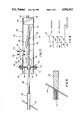
- FIG. 1 is a perspective view of a test station for testing various electronic circuit components employing probe assemblies embodying various aspects of the present invention
- FIG. 2 is an enlarged plan view showing a portion of the top surface of a semiconductor device, certain target areas of which are to be contacted by the probe assemblies of FIG. 1;
- FIG. 3 is a perspective view of the probe assembly of FIG. 1 with a portion of a housing cut away to expose underlying components;
- FIG. 4 is a cross sectional view taken generally along line 4--4 of FIG. 3 showing a contact block disposed inside the housing biased into engagement with a lower contact;
- FIG. 5 similar to FIG. 4, illustrates the contact block moved out of engagement with the lower contact and into, engagement with an upper contact
- FIG. 6 is a sectional view taken generally along line 6--6 of FIG. 3 showing details of a probe holder and a probe point;
- FIG. 7 is a side elevational view of the probe assembly with a portion of the housing cut away to show an electrical connector fixed to the housing and having terminal elements connected to various components of the probe assembly;
- FIG. 8 is an electrical schematic diagram of the probe assembly illustrating a normally closed set of contacts, a normally open set of contacts, and a connection to the probe point.
- a probe assembly for use at a test station 22 for contacting a predetermined target on an electrical circuitry component is generally indicated by reference numeral 20.
- the test station could include a number of manipulators 24 each of which holds and controls movement of a corresponding probe assembly 20.
- An example of such a test station is Model 7000 available from the Micromanipulator Company, Inc. of Carson City, Nev.
- FIG. 2 shows greatly enlarged a portion of an electrical circuitry component which could be tested using the station 22.
- the component 26 could include an integrated circuit chip having a top surface 28 including contact points 30 and conductive paths 32.
- the probe assembly 20 includes an elongated tubular housing 34, preferably of rectangular cross section, including a first end 36, a second end 38, and defining a cavity 40 extending between the ends.
- a base 42 of relatively rigid insulative material, such as delrin, is held in the housing adjacent the second end 38.
- the probe assembly is connected to its corresponding manipulator 24 by a rigid shank 43 held in the base 42.
- a contact block 44 is located in the housing cavity adjacent the first end 36 with an interior beam assembly 46 interconnecting the base and the block so that the block is supported by the base.
- the contact block is also formed of a relatively rigid insulating material, preferably delrin, but with an electrically conductive coating on the top surface 48 and bottom surface 50 of the contact block.
- the interior beam assembly 46 includes a short length of a rigid beam 52 extending from the base 42, a second short length of rigid beam 54 extending from the contact block 44 toward the base, and a somewhat stiff but relatively flexible cantilever beam 56 joining the rigid beams.
- This flexible beam is preferably formed of tungsten and its flexibility can be varied be changing its diameter.
- the probe assembly also includes a relatively rigid second beam assembly 58 extending from the contact block 44 beyond the housing first end 36. This beam assembly could include an extension of beam 54 connected to a probe holder 59. A probe point 60, for engaging the circuitry target, is held by the probe holder, as shown in FIG. 6.
- the probe assembly 20 further includes an upper contact 62 held by the housing 34 in alignment with the contact block top surface 48 and extending into the cavity 40 toward the contact block.
- assembly 20 includes a lower contact 64 held by the housing in alignment with the contact block lower surface 50 and extending upwardly into the cavity toward the contact block.
- the upper contact includes a nut 66 affixed to the housing over an aperture in the housing and a set screw 68 threadably carried by the nut.
- the lower contact 64 is similar, comprising a nut 70 and a set screw 72 threadably carried by the nut 70.
- a connector 74 mounteded on the top wall of the housing over an opening in the top wall between the ends of the housing is a connector 74 including an insulative body 76 and four spaced terminal elements 78-84.
- the first terminal element 78 is connected to the first rigid beam 52 of the interior beam assembly by a first thin wire 86.
- the first terminal element 78 provides a connection to the probe point 60.
- the second terminal element 80 and the fourth terminal element 84 are connected to the conductive bottom surface 50 and to the conductive top surface 48 of the contact block 44 by thin conductors 88 and 90, respectively.
- the housing 34 is connected to the third terminal element 82 by a thin conductor 92.
- the third terminal element is electrically connected to the upper contact 62 and to the lower contact 64 because the housing, the nuts 66 and 70, and the set screws 68 and 72 are all electrically conductive or have electrically conductive coatings.
- the rigid beam 54 is spaced from the conductive upper and lower surfaces 48 and 50 by insulative portions of the contact block 44. Additionally the height of the contact block is somewhat less than the spacing between the distal ends of the set screws 68 and 72. As shown in FIG. 4, when the probe point 60 does not engage the target of the circuitry component, the contact block rests lightly on the lower set screw 72. Thus as shown in the electrical schematic diagram of FIG. 8, terminal elements 80 and 82 are connected to a normally closed set of contacts. When the probe point 60 is lowered into engagement with the circuitry target, the contact block 44 is moved out of engagement with lower screw 72 causing the normally closed set of contacts 80, 82 to open.
- the probe assembly 20 not only includes a touchdown sensor for providing a switched output (opening of the normally closed contacts) indicating that contact with the target area has been established, but also includes a force control. That is, once the desired force which the probe point is to apply against the target is determined, the probe assembly can be adjusted to provide a second switched output (closing of the normally open contacts) to indicate that the force has been achieved. The use of the second switched output to stop application of additional force guards against damage to both the circuitry component and to the probe point.
- the predetermined force for contact closing can conveniently be adjusted by movement of the upper set screw to adjust the deflection distance of the contact block.
- the housing 34 functions as a rigid support for the beam assemblies and the set screws of the upper and lower switches.
- the housing is preferably rectangular in cross section and may have a width of 3/16 inch, a height of 3/8 inch, a length of two inches long and be formed of a thin wall brass tube.
- the shank 43 could be made of aluminum and be 1/8 inch in diameter and 3/8 inch long.
- the nuts 66 and 70 are preferably lock nuts, 2-56 nylon lock rim steel nuts. The nuts are glued over holes in the housing using conductive epoxy.
- the housing with the nuts in place is preferably gold plated for conductivity and lowered contact resistance.
- Both the upper and lower set screws 68 and 72 are round point 2-56 hex drive and are gold plated.
- the upper screw could be about 3/8 inch long and the lower screw about 1/4 inch long.
- the connector 74 or feed through header provides an anchor for the fine wires 86-92 that connect the internal parts of the probe assembly. These wires are preferably 36 gauge magnet wire, except that the wire 86 to the first terminal 78 is preferably 30 gauge plastic insulated to carry the signal to or from the probe point 60.
- the connector or header may be attached to outside equipment by a four wire flat ribbon cable, and also provides strain relief for the external cable.
- the active element of the probe assembly 20 is the flexible cantilever beam 56 which could have a diameter of about 2/100 of an inch and a length of about 3/4 inch.
- the flexible beam 56 is preferably soldered to the ends of the first and second rigid beams 52 and 54.
- the flexible cantilever beam 56 is held in the insulating base 42 by the first rigid beam 52 which has a length of about 1/2 inch and is formed of about 1/16 inch diameter stainless steel tube.
- This beam 52 provides a non-moving attachment for the flexible beam and the signal wire 86 for electrical connection to the probe point.
- the flexible beam 56 is sufficiently stiff to hold the weight of the probe holder 59 so that the normally closed switch has very little weight on it.
- the flexible beam is also sufficiently flexible so that only a few milligrams of force will deflect the probe point to open the normally closed set of contacts.
- the maximum deflection force of the cantilever may be about 10 grams.
- the second rigid beam 54 extends from the flex beam 56 out to the second beam assembly 58 through the contact block 44. This beam is preferably of 1/16 inch diameter stainless steel tube and is about 11/4 inches long, including a portion of the second beam assembly.
- the upper and lower surfaces 48 and 50 of the contact block may have a gold plated brass shim contact pad glued to them.
- the fine wires soldered to the contact pads extend in a gentle bend to the connector 74.
- the probe holder 59 is made of a 1/8 inch diameter stainless steel having a length of about 11/4 inches.
- the probe point 60 is held in a small opening drilled at about a 45 degree angle through the probe holder 59 and secured by a 2-56 set screw 61.
- the probe holder and exposed rigid beam may be gold plated for appearance and to facilitate electrical contact of the probe point in the probe holder.
- the lower switch can be set using setscrew 72.
- an indicator such as a continuity meter or low voltage light and battery connected to terminals 80 and 82
- the setscrew 72 is brought up until contact is first made.
- the probe housing 34 must be horizontal and the setup location free of vibration. The closer the screw 72 is to the "just touching" position the more sensitive the probe will be to indicating when the point 60 actually touches the substrate and changes the loading on this switch (N.C.).
- the top switch (N.O.) can be set.
- the gap can be set very close.
- Setscrew 68 is brought down until the indicator comes on then backed off, turned counterclockwise a few degrees. As small a gap as possible should be provided without the switch closing.
- This setup is then checked by viewing the probe point under the microscope, at an appropriate power for the point radius to judge that the overdrive or skate of the point is not excessive.
- the N.O. switch may be adjusted by trial and error until the desired force is applied on the point when the N.O. switch closes.
- probe assemblies 20 For a test station that uses a computer controlled Z axis, only one of the probe assemblies 20 is needed for touchdown sensing. If other probes are required, they can be regular passive probes (without the touch down sensor feature).
- the probe point 60 When probing in manual or automatic modes it may be necessary to overdrive the probe point 60 after initial contact to establish good electrical contact with the substrate. As indicated by inspection using a microscope, the probe point 60 moves vertically down until it makes contact. It then slides forward upon the substrate several point diameters. The amount of slide is a function of the amount of vertical overdrive. Factors contributing to the amount of overdrive needed are the continuity and resistivity of the contact, the point radius of the probe, and the geometry of the substrate.
- the contact probe With the contact probe it is possible to sense when the probe point makes contact with the substrate and, also, when a preset amount of overdrive is reached, without visual feedback from an operator. Its uses are as an adjunct to an operator to facilitate repetitive operations or as an input to an automated system with Z axis position control.
Abstract
Description
Claims (10)
Priority Applications (1)
| Application Number | Priority Date | Filing Date | Title |
|---|---|---|---|
| US07/433,021 US4956923A (en) | 1989-11-06 | 1989-11-06 | Probe assembly including touchdown sensor |
Applications Claiming Priority (1)
| Application Number | Priority Date | Filing Date | Title |
|---|---|---|---|
| US07/433,021 US4956923A (en) | 1989-11-06 | 1989-11-06 | Probe assembly including touchdown sensor |
Publications (1)
| Publication Number | Publication Date |
|---|---|
| US4956923A true US4956923A (en) | 1990-09-18 |
Family
ID=23718538
Family Applications (1)
| Application Number | Title | Priority Date | Filing Date |
|---|---|---|---|
| US07/433,021 Expired - Fee Related US4956923A (en) | 1989-11-06 | 1989-11-06 | Probe assembly including touchdown sensor |
Country Status (1)
| Country | Link |
|---|---|
| US (1) | US4956923A (en) |
Cited By (23)
| Publication number | Priority date | Publication date | Assignee | Title |
|---|---|---|---|---|
| US5446393A (en) * | 1993-05-21 | 1995-08-29 | Schaefer; Richard K. | Electrical measuring and testing probe having a malleable shaft facilitating positioning of a contact pin |
| US5850146A (en) * | 1995-12-30 | 1998-12-15 | Samsung Electronics Co., Ltd. | Probe apparatus for electrical inspection of printed circuit board assembly |
| US6014032A (en) * | 1997-09-30 | 2000-01-11 | International Business Machines Corporation | Micro probe ring assembly and method of fabrication |
| US6016607A (en) * | 1997-03-27 | 2000-01-25 | Sandia Corporation | Coordinated X-Y stage apparatus |
| US6059982A (en) * | 1997-09-30 | 2000-05-09 | International Business Machines Corporation | Micro probe assembly and method of fabrication |
| US6139759A (en) * | 1997-07-08 | 2000-10-31 | International Business Machines Corporation | Method of manufacturing silicided silicon microtips for scanning probe microscopy |
| US6327789B1 (en) * | 1998-08-04 | 2001-12-11 | Mitutoyo Corp. | Touch signal probe |
| US6369592B1 (en) * | 1999-05-24 | 2002-04-09 | International Business Machines Corporation | Probe for testing and repairing printed circuit features |
| US20030121165A1 (en) * | 2001-12-21 | 2003-07-03 | Magna International Inc. | Electronic measuring device |
| WO2003071288A1 (en) * | 2002-02-20 | 2003-08-28 | Ismeca Semiconductor Holding Sa | Contact actuator with contact force control |
| US6815961B2 (en) | 1999-07-28 | 2004-11-09 | Nanonexus, Inc. | Construction structures and manufacturing processes for integrated circuit wafer probe card assemblies |
| US20050184028A1 (en) * | 2004-02-23 | 2005-08-25 | Zyvex Corporation | Probe tip processing |
| US20050223968A1 (en) * | 2004-03-26 | 2005-10-13 | Zyvex Corporation | Patterned atomic layer epitaxy |
| US7009412B2 (en) | 1999-05-27 | 2006-03-07 | Nanonexus, Inc. | Massively parallel interface for electronic circuit |
| DE10207878B4 (en) * | 2001-02-23 | 2006-05-11 | Göpel electronic GmbH | Device for detecting, holding and checking electronic assemblies |
| US20070001693A1 (en) * | 2001-12-07 | 2007-01-04 | Atg Test Systems Gmbh & Co. Kg | Test probe for finger tester and corresponding finger tester |
| CN1320698C (en) * | 2002-02-20 | 2007-06-06 | 伊斯梅卡半导体控股公司 | System for actuating electronic component contactor containing contact force controlling mechanism |
| US7349223B2 (en) | 2000-05-23 | 2008-03-25 | Nanonexus, Inc. | Enhanced compliant probe card systems having improved planarity |
| US7382142B2 (en) | 2000-05-23 | 2008-06-03 | Nanonexus, Inc. | High density interconnect system having rapid fabrication cycle |
| US20080165344A1 (en) * | 2005-07-14 | 2008-07-10 | Chemimage Corporation | System and system for robot mounted sensor |
| US7579848B2 (en) | 2000-05-23 | 2009-08-25 | Nanonexus, Inc. | High density interconnect system for IC packages and interconnect assemblies |
| US7621761B2 (en) | 2000-06-20 | 2009-11-24 | Nanonexus, Inc. | Systems for testing and packaging integrated circuits |
| US7952373B2 (en) | 2000-05-23 | 2011-05-31 | Verigy (Singapore) Pte. Ltd. | Construction structures and manufacturing processes for integrated circuit wafer probe card assemblies |
Citations (18)
| Publication number | Priority date | Publication date | Assignee | Title |
|---|---|---|---|---|
| US2011931A (en) * | 1931-12-05 | 1935-08-20 | Western Electric Co | Gauging apparatus |
| US2417148A (en) * | 1943-08-02 | 1947-03-11 | Gen Motors Corp | Dimension gauging means |
| US2707333A (en) * | 1949-05-06 | 1955-05-03 | Schaurte Paul | Electrical comparator |
| US3076069A (en) * | 1960-04-04 | 1963-01-29 | Rca Corp | Combined sensing and switching device |
| US3171012A (en) * | 1962-03-26 | 1965-02-23 | Laurel A Morehead | Automatic groove follower for welding apparatus |
| US3243186A (en) * | 1964-06-08 | 1966-03-29 | Johnson Shelby | Golfer's head movement indicator |
| US3258571A (en) * | 1964-12-31 | 1966-06-28 | Guardian Electric Mfg Co | Slide-on lifter for switch blades |
| US3488461A (en) * | 1967-12-21 | 1970-01-06 | Webb James E | Deflective rod switch with elastic support and sealing means |
| US3551807A (en) * | 1968-10-01 | 1970-12-29 | Pennwalt Corp | Manually adjustable electrical probe for testing printed circuits and the like |
| US3742610A (en) * | 1970-02-16 | 1973-07-03 | Genevoise Instr Physique | Measuring device of two dimensional displacements |
| US3750295A (en) * | 1971-07-22 | 1973-08-07 | Werkzeugmasch Veb | Measuring machine |
| US3849614A (en) * | 1973-05-14 | 1974-11-19 | Calc Securities Syst Inc | Tamper switch device for detection of relative motion |
| US4123706A (en) * | 1975-03-03 | 1978-10-31 | Electroglas, Inc. | Probe construction |
| US4382228A (en) * | 1974-07-15 | 1983-05-03 | Wentworth Laboratories Inc. | Probes for fixed point probe cards |
| US4523063A (en) * | 1983-12-05 | 1985-06-11 | Gte Valeron Corporation | Touch probe having nonconductive contact carriers |
| US4542590A (en) * | 1984-03-26 | 1985-09-24 | Gte Valeron Corporation | Two axis touch probe |
| US4553332A (en) * | 1982-10-18 | 1985-11-19 | Finike Italiana Marposs S.P.A. | Probe for checking linear dimensions |
| US4575947A (en) * | 1983-03-30 | 1986-03-18 | Wyler Ag | Measuring arm for a multiple coordinate measuring machine |
-
1989
- 1989-11-06 US US07/433,021 patent/US4956923A/en not_active Expired - Fee Related
Patent Citations (18)
| Publication number | Priority date | Publication date | Assignee | Title |
|---|---|---|---|---|
| US2011931A (en) * | 1931-12-05 | 1935-08-20 | Western Electric Co | Gauging apparatus |
| US2417148A (en) * | 1943-08-02 | 1947-03-11 | Gen Motors Corp | Dimension gauging means |
| US2707333A (en) * | 1949-05-06 | 1955-05-03 | Schaurte Paul | Electrical comparator |
| US3076069A (en) * | 1960-04-04 | 1963-01-29 | Rca Corp | Combined sensing and switching device |
| US3171012A (en) * | 1962-03-26 | 1965-02-23 | Laurel A Morehead | Automatic groove follower for welding apparatus |
| US3243186A (en) * | 1964-06-08 | 1966-03-29 | Johnson Shelby | Golfer's head movement indicator |
| US3258571A (en) * | 1964-12-31 | 1966-06-28 | Guardian Electric Mfg Co | Slide-on lifter for switch blades |
| US3488461A (en) * | 1967-12-21 | 1970-01-06 | Webb James E | Deflective rod switch with elastic support and sealing means |
| US3551807A (en) * | 1968-10-01 | 1970-12-29 | Pennwalt Corp | Manually adjustable electrical probe for testing printed circuits and the like |
| US3742610A (en) * | 1970-02-16 | 1973-07-03 | Genevoise Instr Physique | Measuring device of two dimensional displacements |
| US3750295A (en) * | 1971-07-22 | 1973-08-07 | Werkzeugmasch Veb | Measuring machine |
| US3849614A (en) * | 1973-05-14 | 1974-11-19 | Calc Securities Syst Inc | Tamper switch device for detection of relative motion |
| US4382228A (en) * | 1974-07-15 | 1983-05-03 | Wentworth Laboratories Inc. | Probes for fixed point probe cards |
| US4123706A (en) * | 1975-03-03 | 1978-10-31 | Electroglas, Inc. | Probe construction |
| US4553332A (en) * | 1982-10-18 | 1985-11-19 | Finike Italiana Marposs S.P.A. | Probe for checking linear dimensions |
| US4575947A (en) * | 1983-03-30 | 1986-03-18 | Wyler Ag | Measuring arm for a multiple coordinate measuring machine |
| US4523063A (en) * | 1983-12-05 | 1985-06-11 | Gte Valeron Corporation | Touch probe having nonconductive contact carriers |
| US4542590A (en) * | 1984-03-26 | 1985-09-24 | Gte Valeron Corporation | Two axis touch probe |
Cited By (44)
| Publication number | Priority date | Publication date | Assignee | Title |
|---|---|---|---|---|
| US5446393A (en) * | 1993-05-21 | 1995-08-29 | Schaefer; Richard K. | Electrical measuring and testing probe having a malleable shaft facilitating positioning of a contact pin |
| US5850146A (en) * | 1995-12-30 | 1998-12-15 | Samsung Electronics Co., Ltd. | Probe apparatus for electrical inspection of printed circuit board assembly |
| US6016607A (en) * | 1997-03-27 | 2000-01-25 | Sandia Corporation | Coordinated X-Y stage apparatus |
| US6139759A (en) * | 1997-07-08 | 2000-10-31 | International Business Machines Corporation | Method of manufacturing silicided silicon microtips for scanning probe microscopy |
| US6198300B1 (en) | 1997-07-08 | 2001-03-06 | International Business Machines Corporation | Silicided silicon microtips for scanning probe microscopy |
| US6014032A (en) * | 1997-09-30 | 2000-01-11 | International Business Machines Corporation | Micro probe ring assembly and method of fabrication |
| US6059982A (en) * | 1997-09-30 | 2000-05-09 | International Business Machines Corporation | Micro probe assembly and method of fabrication |
| US6232143B1 (en) | 1997-09-30 | 2001-05-15 | International Business Machines Corporation | Micro probe ring assembly and method of fabrication |
| US6327789B1 (en) * | 1998-08-04 | 2001-12-11 | Mitutoyo Corp. | Touch signal probe |
| US6369592B1 (en) * | 1999-05-24 | 2002-04-09 | International Business Machines Corporation | Probe for testing and repairing printed circuit features |
| US7009412B2 (en) | 1999-05-27 | 2006-03-07 | Nanonexus, Inc. | Massively parallel interface for electronic circuit |
| US7884634B2 (en) | 1999-05-27 | 2011-02-08 | Verigy (Singapore) Pte, Ltd | High density interconnect system having rapid fabrication cycle |
| US7403029B2 (en) | 1999-05-27 | 2008-07-22 | Nanonexus Corporation | Massively parallel interface for electronic circuit |
| US7772860B2 (en) | 1999-05-27 | 2010-08-10 | Nanonexus, Inc. | Massively parallel interface for electronic circuit |
| US6815961B2 (en) | 1999-07-28 | 2004-11-09 | Nanonexus, Inc. | Construction structures and manufacturing processes for integrated circuit wafer probe card assemblies |
| US7579848B2 (en) | 2000-05-23 | 2009-08-25 | Nanonexus, Inc. | High density interconnect system for IC packages and interconnect assemblies |
| US7872482B2 (en) | 2000-05-23 | 2011-01-18 | Verigy (Singapore) Pte. Ltd | High density interconnect system having rapid fabrication cycle |
| US7952373B2 (en) | 2000-05-23 | 2011-05-31 | Verigy (Singapore) Pte. Ltd. | Construction structures and manufacturing processes for integrated circuit wafer probe card assemblies |
| US7382142B2 (en) | 2000-05-23 | 2008-06-03 | Nanonexus, Inc. | High density interconnect system having rapid fabrication cycle |
| US7349223B2 (en) | 2000-05-23 | 2008-03-25 | Nanonexus, Inc. | Enhanced compliant probe card systems having improved planarity |
| US7621761B2 (en) | 2000-06-20 | 2009-11-24 | Nanonexus, Inc. | Systems for testing and packaging integrated circuits |
| DE10207878B4 (en) * | 2001-02-23 | 2006-05-11 | Göpel electronic GmbH | Device for detecting, holding and checking electronic assemblies |
| US7355424B2 (en) * | 2001-12-07 | 2008-04-08 | Atg Test Systems Gmbh & Co. Kg | Test probe for finger tester and corresponding finger tester |
| US20070001693A1 (en) * | 2001-12-07 | 2007-01-04 | Atg Test Systems Gmbh & Co. Kg | Test probe for finger tester and corresponding finger tester |
| USRE43739E1 (en) | 2001-12-07 | 2012-10-16 | Atg Luther & Maelzer Gmbh | Test probe for finger tester and corresponding finger tester |
| US20030121165A1 (en) * | 2001-12-21 | 2003-07-03 | Magna International Inc. | Electronic measuring device |
| US6804896B2 (en) * | 2001-12-21 | 2004-10-19 | Magna International Inc. | Electronic measuring device |
| CN1320698C (en) * | 2002-02-20 | 2007-06-06 | 伊斯梅卡半导体控股公司 | System for actuating electronic component contactor containing contact force controlling mechanism |
| CN100437122C (en) * | 2002-02-20 | 2008-11-26 | 伊斯梅卡半导体控股公司 | Contact actuator with contact force controlling mechanism |
| WO2003071288A1 (en) * | 2002-02-20 | 2003-08-28 | Ismeca Semiconductor Holding Sa | Contact actuator with contact force control |
| US20050011027A1 (en) * | 2002-02-20 | 2005-01-20 | Ismeca Semiconductor Holding Sa | Contact actuator with contact force control |
| US20060192116A1 (en) * | 2004-02-23 | 2006-08-31 | Zyvex Corporation | Charged particle beam device probe operation |
| US7319336B2 (en) | 2004-02-23 | 2008-01-15 | Zyvex Instruments, Llc | Charged particle beam device probe operation |
| US7285778B2 (en) | 2004-02-23 | 2007-10-23 | Zyvex Corporation | Probe current imaging |
| US7675300B2 (en) | 2004-02-23 | 2010-03-09 | Zyvex Instruments, Llc | Charged particle beam device probe operation |
| US20050184236A1 (en) * | 2004-02-23 | 2005-08-25 | Zyvex Corporation | Probe current imaging |
| US20050184028A1 (en) * | 2004-02-23 | 2005-08-25 | Zyvex Corporation | Probe tip processing |
| US20080150557A1 (en) * | 2004-02-23 | 2008-06-26 | Zyvex Instruments, Llc | Charged particle beam device probe operation |
| US20080092803A1 (en) * | 2004-03-26 | 2008-04-24 | Zyvex Labs, Llc | Patterned atomic layer epitaxy |
| US20050223968A1 (en) * | 2004-03-26 | 2005-10-13 | Zyvex Corporation | Patterned atomic layer epitaxy |
| US7799132B2 (en) | 2004-03-26 | 2010-09-21 | Zyvex Labs, Llc | Patterned atomic layer epitaxy |
| US7326293B2 (en) | 2004-03-26 | 2008-02-05 | Zyvex Labs, Llc | Patterned atomic layer epitaxy |
| US7420664B2 (en) * | 2005-07-14 | 2008-09-02 | Chemimage Corporation | System and method for robot mounted sensor |
| US20080165344A1 (en) * | 2005-07-14 | 2008-07-10 | Chemimage Corporation | System and system for robot mounted sensor |
Similar Documents
| Publication | Publication Date | Title |
|---|---|---|
| US4956923A (en) | Probe assembly including touchdown sensor | |
| US4758785A (en) | Pressure control apparatus for use in an integrated circuit testing station | |
| US3609539A (en) | Self-aligning kelvin probe | |
| US4673839A (en) | Piezoelectric pressure sensing apparatus for integrated circuit testing stations | |
| US4123706A (en) | Probe construction | |
| US4764722A (en) | Coaxial probe | |
| US6043668A (en) | Planarity verification system for integrated circuit test probes | |
| US5012186A (en) | Electrical probe with contact force protection | |
| US4047780A (en) | Test contactor system for semiconductor device handling apparatus | |
| US6023171A (en) | Dual-contact probe tip for flying probe tester | |
| US7868635B2 (en) | Probe | |
| US6653825B2 (en) | Meter lead holder device | |
| US5446393A (en) | Electrical measuring and testing probe having a malleable shaft facilitating positioning of a contact pin | |
| US6263585B1 (en) | Caliper probe-measuring device | |
| US6069480A (en) | Kelvin contact-type testing device | |
| JP2000028673A (en) | Printed wiring board substrate-testing device | |
| US7733107B1 (en) | Charged device model contact plate | |
| US4812745A (en) | Probe for testing electronic components | |
| US5045710A (en) | Coplanarity inspection machine | |
| JP2000131340A (en) | Contact probe device | |
| KR20020025786A (en) | Calibration Device for Semiconductor Testing Apparatus, Calibration Method and Semiconductor Testing Apparatus | |
| US4776102A (en) | Tool for measuring the height of a material buildup on a reference plane | |
| JPH0854403A (en) | Conductive cantilever structure of compound microscope | |
| JP6000046B2 (en) | Probe unit and inspection device | |
| US6369592B1 (en) | Probe for testing and repairing printed circuit features |
Legal Events
| Date | Code | Title | Description |
|---|---|---|---|
| AS | Assignment |
Owner name: MICROMANIPULATOR COMPANY, INC., THE, NEVADA Free format text: ASSIGNMENT OF ASSIGNORS INTEREST.;ASSIGNORS:PETTINGELL, JAMES T.;HOLLMAN, KENNETH F.;REEL/FRAME:005174/0381;SIGNING DATES FROM 19891016 TO 19891031 |
|
| CC | Certificate of correction | ||
| FEPP | Fee payment procedure |
Free format text: PAYOR NUMBER ASSIGNED (ORIGINAL EVENT CODE: ASPN); ENTITY STATUS OF PATENT OWNER: SMALL ENTITY |
|
| FPAY | Fee payment |
Year of fee payment: 4 |
|
| FPAY | Fee payment |
Year of fee payment: 8 |
|
| REMI | Maintenance fee reminder mailed | ||
| LAPS | Lapse for failure to pay maintenance fees | ||
| STCH | Information on status: patent discontinuation |
Free format text: PATENT EXPIRED DUE TO NONPAYMENT OF MAINTENANCE FEES UNDER 37 CFR 1.362 |
|
| FP | Lapsed due to failure to pay maintenance fee |
Effective date: 20020918 |
|
| AS | Assignment |
Owner name: SILICON VALLEY BANK, CALIFORNIA Free format text: ASSIGNMENT OF ASSIGNORS INTEREST;ASSIGNOR:MICROMANIPULATOR CO., INC., THE;REEL/FRAME:017411/0306 Effective date: 20051220 |
|
| AS | Assignment |
Owner name: MICROMANIPULATOR CO., INC., THE, NEVADA Free format text: RELEASE;ASSIGNOR:SILICON VALLEY BANK;REEL/FRAME:026669/0914 Effective date: 20110714 |