US4958205A - Thin film transistor array and method of manufacturing the same - Google Patents
Thin film transistor array and method of manufacturing the same Download PDFInfo
- Publication number
- US4958205A US4958205A US07/188,623 US18862388A US4958205A US 4958205 A US4958205 A US 4958205A US 18862388 A US18862388 A US 18862388A US 4958205 A US4958205 A US 4958205A
- Authority
- US
- United States
- Prior art keywords
- semiconductor layer
- disposed
- insulating layer
- layer
- impurity
- Prior art date
- Legal status (The legal status is an assumption and is not a legal conclusion. Google has not performed a legal analysis and makes no representation as to the accuracy of the status listed.)
- Expired - Lifetime
Links
- 239000010409 thin film Substances 0.000 title claims description 8
- 238000004519 manufacturing process Methods 0.000 title abstract description 7
- 239000004065 semiconductor Substances 0.000 claims abstract description 45
- 230000001681 protective effect Effects 0.000 claims abstract description 21
- 239000004973 liquid crystal related substance Substances 0.000 claims abstract description 5
- 229910052751 metal Inorganic materials 0.000 claims description 24
- 239000002184 metal Substances 0.000 claims description 24
- 239000000758 substrate Substances 0.000 claims description 13
- 230000004888 barrier function Effects 0.000 claims description 6
- 239000000463 material Substances 0.000 claims description 2
- 238000000034 method Methods 0.000 abstract description 11
- 238000000059 patterning Methods 0.000 abstract description 6
- 239000010408 film Substances 0.000 description 20
- 238000005268 plasma chemical vapour deposition Methods 0.000 description 5
- 229910021417 amorphous silicon Inorganic materials 0.000 description 4
- 238000003491 array Methods 0.000 description 4
- 239000011651 chromium Substances 0.000 description 4
- 239000011248 coating agent Substances 0.000 description 3
- 238000000576 coating method Methods 0.000 description 3
- 238000005530 etching Methods 0.000 description 3
- VYZAMTAEIAYCRO-UHFFFAOYSA-N Chromium Chemical compound [Cr] VYZAMTAEIAYCRO-UHFFFAOYSA-N 0.000 description 2
- 229910052804 chromium Inorganic materials 0.000 description 2
- 238000007796 conventional method Methods 0.000 description 2
- 239000010936 titanium Substances 0.000 description 2
- 229910000838 Al alloy Inorganic materials 0.000 description 1
- 229910052581 Si3N4 Inorganic materials 0.000 description 1
- 229910004205 SiNX Inorganic materials 0.000 description 1
- RTAQQCXQSZGOHL-UHFFFAOYSA-N Titanium Chemical compound [Ti] RTAQQCXQSZGOHL-UHFFFAOYSA-N 0.000 description 1
- 229910052782 aluminium Inorganic materials 0.000 description 1
- XAGFODPZIPBFFR-UHFFFAOYSA-N aluminium Chemical compound [Al] XAGFODPZIPBFFR-UHFFFAOYSA-N 0.000 description 1
- 238000000151 deposition Methods 0.000 description 1
- 230000008021 deposition Effects 0.000 description 1
- 230000000694 effects Effects 0.000 description 1
- 239000012535 impurity Substances 0.000 description 1
- 239000011159 matrix material Substances 0.000 description 1
- 230000003071 parasitic effect Effects 0.000 description 1
- 229920002120 photoresistant polymer Polymers 0.000 description 1
- HQVNEWCFYHHQES-UHFFFAOYSA-N silicon nitride Chemical compound N12[Si]34N5[Si]62N3[Si]51N64 HQVNEWCFYHHQES-UHFFFAOYSA-N 0.000 description 1
- 238000004544 sputter deposition Methods 0.000 description 1
- 229910052719 titanium Inorganic materials 0.000 description 1
- WFKWXMTUELFFGS-UHFFFAOYSA-N tungsten Chemical compound [W] WFKWXMTUELFFGS-UHFFFAOYSA-N 0.000 description 1
- 229910052721 tungsten Inorganic materials 0.000 description 1
- 239000010937 tungsten Substances 0.000 description 1
Images


Classifications
-
- H—ELECTRICITY
- H01—ELECTRIC ELEMENTS
- H01L—SEMICONDUCTOR DEVICES NOT COVERED BY CLASS H10
- H01L29/00—Semiconductor devices adapted for rectifying, amplifying, oscillating or switching, or capacitors or resistors with at least one potential-jump barrier or surface barrier, e.g. PN junction depletion layer or carrier concentration layer; Details of semiconductor bodies or of electrodes thereof ; Multistep manufacturing processes therefor
- H01L29/40—Electrodes ; Multistep manufacturing processes therefor
- H01L29/43—Electrodes ; Multistep manufacturing processes therefor characterised by the materials of which they are formed
- H01L29/45—Ohmic electrodes
- H01L29/456—Ohmic electrodes on silicon
- H01L29/458—Ohmic electrodes on silicon for thin film silicon, e.g. source or drain electrode
-
- G—PHYSICS
- G02—OPTICS
- G02F—OPTICAL DEVICES OR ARRANGEMENTS FOR THE CONTROL OF LIGHT BY MODIFICATION OF THE OPTICAL PROPERTIES OF THE MEDIA OF THE ELEMENTS INVOLVED THEREIN; NON-LINEAR OPTICS; FREQUENCY-CHANGING OF LIGHT; OPTICAL LOGIC ELEMENTS; OPTICAL ANALOGUE/DIGITAL CONVERTERS
- G02F1/00—Devices or arrangements for the control of the intensity, colour, phase, polarisation or direction of light arriving from an independent light source, e.g. switching, gating or modulating; Non-linear optics
- G02F1/01—Devices or arrangements for the control of the intensity, colour, phase, polarisation or direction of light arriving from an independent light source, e.g. switching, gating or modulating; Non-linear optics for the control of the intensity, phase, polarisation or colour
- G02F1/13—Devices or arrangements for the control of the intensity, colour, phase, polarisation or direction of light arriving from an independent light source, e.g. switching, gating or modulating; Non-linear optics for the control of the intensity, phase, polarisation or colour based on liquid crystals, e.g. single liquid crystal display cells
- G02F1/133—Constructional arrangements; Operation of liquid crystal cells; Circuit arrangements
- G02F1/136—Liquid crystal cells structurally associated with a semi-conducting layer or substrate, e.g. cells forming part of an integrated circuit
- G02F1/1362—Active matrix addressed cells
- G02F1/1368—Active matrix addressed cells in which the switching element is a three-electrode device
-
- H—ELECTRICITY
- H01—ELECTRIC ELEMENTS
- H01L—SEMICONDUCTOR DEVICES NOT COVERED BY CLASS H10
- H01L29/00—Semiconductor devices adapted for rectifying, amplifying, oscillating or switching, or capacitors or resistors with at least one potential-jump barrier or surface barrier, e.g. PN junction depletion layer or carrier concentration layer; Details of semiconductor bodies or of electrodes thereof ; Multistep manufacturing processes therefor
- H01L29/66—Types of semiconductor device ; Multistep manufacturing processes therefor
- H01L29/68—Types of semiconductor device ; Multistep manufacturing processes therefor controllable by only the electric current supplied, or only the electric potential applied, to an electrode which does not carry the current to be rectified, amplified or switched
- H01L29/76—Unipolar devices, e.g. field effect transistors
- H01L29/772—Field effect transistors
- H01L29/78—Field effect transistors with field effect produced by an insulated gate
- H01L29/786—Thin film transistors, i.e. transistors with a channel being at least partly a thin film
- H01L29/78651—Silicon transistors
- H01L29/7866—Non-monocrystalline silicon transistors
- H01L29/78663—Amorphous silicon transistors
- H01L29/78669—Amorphous silicon transistors with inverted-type structure, e.g. with bottom gate
-
- Y—GENERAL TAGGING OF NEW TECHNOLOGICAL DEVELOPMENTS; GENERAL TAGGING OF CROSS-SECTIONAL TECHNOLOGIES SPANNING OVER SEVERAL SECTIONS OF THE IPC; TECHNICAL SUBJECTS COVERED BY FORMER USPC CROSS-REFERENCE ART COLLECTIONS [XRACs] AND DIGESTS
- Y10—TECHNICAL SUBJECTS COVERED BY FORMER USPC
- Y10S—TECHNICAL SUBJECTS COVERED BY FORMER USPC CROSS-REFERENCE ART COLLECTIONS [XRACs] AND DIGESTS
- Y10S438/00—Semiconductor device manufacturing: process
- Y10S438/942—Masking
- Y10S438/948—Radiation resist
- Y10S438/949—Energy beam treating radiation resist on semiconductor
Definitions
- This invention relates to a thin film transistor (TFT) array used for driving pixels in active matrix type liquid crystal display (LCD) devices and a method of manufacturing the same.
- TFT thin film transistor
- TFT arrays have recently been used in LCD devices having a large number of pixels for constituting a high contrast display.
- Typical conventional methods for producing TFT arrays are disclosed in Japanese Laid-Open Patent Applications No. 58-14568 and No. 59-113667. These methods comprise a self alignment process and a lift-off process.
- the lift-off process is used for forming the impurity-doped semiconductor layer and the source and drain electrodes by using a resist on the protective insulating layer above the TFT channel portion.
- it was difficult to activate the impurity in the intrinsic semiconductor layer because of the deposition at a low temperature.
- the TFT array is further required to have such a structure that undesired parastic capacitances should be as small as possible and that the channel portion should be subjected to less external light.
- An object of the present invention is to provide a TFT array with reduced parastic capacitances.
- Another object of the present invention is to provide a TFT array the channel portion of which is subjected to less external light.
- a further object of the present invention is to provide an easy method of producing a TFT array.
- a still further object of the present invention is to produce a self-aligned TFT array without using the lift-off process.
- an insulative layer for protecting the channel portion and an impurity-doped semiconductor layer on the insulative layer are patterned by self-alignment by using a gate electrode pattern as a photomask.
- a metal layer may also be formed on the impurity-doped semiconductor layer and is also patterned by self-alignment along with the insulative layer and the impurity-doped semiconductor layer.
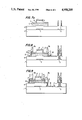
- FIG. 1 is a partial sectional view showing an embodiment of a self-aligned TFT array according to the present invention
- FIGS. 2a, 2b, 2c, 2d, 2e, 2f and 2g are partial sectional views showing a manufacturing process of the TFT array in FIG. 1;
- FIGS. 3, 4 and 5 are partial sectional views showing embodiments of self-aligned TFT arrays each having a pixel electrode according to the present invention
- FIG. 6 is a partial sectional view showing another embodiment of a self-aligned TFT array according to the present invention.
- FIGS. 7a, 7b and 7c are partial sectional views showing a manufacturing process of the TFT array in FIG. 6;
- FIGS. 8, 9 and 10 are partial sectional views showing other embodiments of self-aligned TFT arrays each having a pixel electrode according to the present invention.
- reference numeral 1 denotes a transparent insulating substrate; 2 a gate electrode formed on the substrate 1; 3 a gate electrode taking-out terminal (gate terminal) formed on the substrate 1; 4 a gate insulating layer formed on the substrate 1, gate electrode 2 and the gate terminal 3; 5 a semiconductor layer formed on the gate insulating layer 4; 6 a protective insulating layer formed on the semiconductor layer 5 above the TFT channel portion; 7 an impurity-doped semiconductor layer formed on the semiconductor layer 5; 8 a barrier metal layer formed to cover the semiconductor layers 5, 7, a part of the protective insulating layer 6 and a part of the gate insulating layer 4; 9a and 9b are source and drain electrodes, respectively, formed on the metal layer 8.
- the semiconductor layer 5 may be an amorphous silicon (a-Si) layer formed by plasma CVD.
- the impurity-doped semiconductor layer 7 may be a PH 3 -doped a-Si (n + :a-Si) layer.
- Each of the insulating layers 4 and 6 may be a silicon nitride (SiNx) layer formed by plasma CVD.
- the protective insulating layer 6 is provided for protecting the TFT channel portion.
- the source and drain electrodes 9a and 9b are usually made of aluminum (Al) or Al alloy.
- the barrier metal layer 8 may be made of titanium (Ti), tungsten (W) or chromium (Cr) and is provided for preventing the material of the source and drain electrodes from diffusing into the semiconductor layers.
- the pattern of the protective insulating layer 6 is aligned with the pattern of the gate electrode 2, and the impurity-doped semiconductor layer 7 is aligned with the portion which does not include the gate electrode 2.
- the TFT array in FIG. 1 is manufactured by the following manufacturing process:
- Step 1 Forming the gate insulating layer 4, semiconductor layer 5 and protective insulating layer 6 in turn on the insulating substrate 1 provided thereon with the gate electrode 2 each by plasma CVD as shown in FIG. 2a.
- Step 2 Coating the protective insulating layer 6 with a positive resist film 13, and exposing the resist film 13 to light radiating from the lower side (the substrate 1 end) so as to use the gate electrode 2 as a photomask.
- the portion of the resist film 13 above the gate terminal 3 is exposed by a conventional photomask.
- the resist film 13 is developed to form a pattern as shown in FIG. 2b in which the portion of the resist film 13 above the gate electrode 2 exactly coincides with and overlies the pattern of the gate electrode 2.
- the protective insulating layer 6 is etched by using the patterned resist film 13 as a mask, and then the resist film 13 is removed as shown in FIG. 2c.
- Step 3 Forming the impurity-doped semiconductor layer 7, on the product obtained by performing step 2, by plasma CVD, coating the layer 7 with a negative resist film 14, exposing the resist film 14 to light radiating from the lower side (substrate 1 end) by using the gate electrode 2 and the gate terminal 3 as a photomask, and developing the resist film 14, thereby obtaining a pattern of the resist film 14 as shown in FIG. 2d in which the removed portions of the resist film 14 is exactly coincided and had overlied with the gate electrode 2 and the gate terminal 3. Thereafter, the portions of the impurity-doped semiconductor layer 7 aligned with the gate electrode 2 and the gate terminal 3 are etched by using the patterned resist film 14 as a mask, which is thereafter removed.
- Step 4 Coating the product obtained by performing step 4 with a positive resist film 15, patterning the resist film 15 into a specified pattern by using a photomask as shown in FIG. 2e, and thereafter etching the impurity-doped semiconductor layer 7 and the semiconductor layer 5 by using the patterned resist film 15 as a mask as shown in FIG. 2f.
- Step 5 Etching the gate insulating layer 4 at the portion on the gate terminal 3 to obtain a window through which the gate terminal is exposed as shown in FIG. 2g.
- Step 6 Forming the barrier metal layer 8 and the metal layer for the source and drain electrodes 9a and 9b, on the product obtained by performing step 5, by sputtering, and patterning the formed layers into the patterns of the source and drain electrodes 9a and 9b, thereby obtaining the TFT array as shown in FIG. 1.
- the protective insulating layer 6 and the impurity-doped semiconductor layer 7 are patterned by the self-alignment method using the gate electrode 2 as the photomask.
- a transparent pixel electrode connected to the drain electrode must be provided as shown in FIGS. 3 to 5.
- a transparent pixel electrode 10 is formed on the gate insulating layer 4.
- the electrode 10 may be formed between the above described steps 4 and 5 or between the above described steps 5 and 6.
- the transparent pixel electrode 10 is formed on the transparent insulating substrate 1.
- the electrode 10 may be formed before the above described step 1, when a protective metal film 12 is formed on the electrode 10 for protecting the electrode 10 during the subsequent process.
- the protective metal film 12 is removed after forming the source and drain electrodes 9a and 9b.
- the transparent pixel electrode 10 is formed partly on the gate insulating layer and partly on the drain electrode 9b after forming the source and drain electrodes 9a and 9b have been formed.
- FIG. 6 shows another embodiment of TFT array according to the invention.
- the protective insulating layer 6 formed on the semiconductor layer 5 is aligned with the gate electrode 2.
- the impurity-doped semiconductor layer 7 is formed on the semiconductor layer 5 and the protective insulating layer 6, and a third metal layer 11 is formed on the impurity-doped semiconductor layer 7.
- the portions of the impurity-doped semiconductor layer 7 and the third metal layer 11 on the protective insulating layer 6 are isolated from the portions of the layers 7 and 11 on the semiconductor layer 5 due to the level difference between the upper surfaces of the layers 7 and 5 so as not to form a parasitic capacitance.
- the third metal layer 11 may be made of chromium (Cr) and is used as a mask for patterning the semiconductor layer 5 and the impurity-doped semiconductor layer 7.
- the third metal layer 11 also provides the effect of preventing the TFT channel portion from being subjected to external light.
- the source and drain electrodes 9a and 9b are disposed so as not to cover the area above the TFT channel portion.
- the TFT array in FIG. 6 can be manufactured by the following manufacturing process:
- Steps 1, 2 Same as steps 1, 2 for the TFT array in FIG. 1.
- Step 3 Forming the impurity-doped semiconductor layer 7 on the product formed by step 2 (FIG. 2c), and forming the third metal layer 11 on the impurity-doped semiconductor layer 7 by plasma CVD.
- the metal layer 11 is formed so as not to cover all of the side surfaces of the patterned protective insulating layer 6.
- a resist film 16 is formed on the metal layer 11 and is patterned into a specific pattern as shown in FIG. 7a.
- Step 4 Patterning the metal layer 11 into the specific pattern by using the resist film 16 as a mask, and etching the impurity-doped semiconductor layer 7 and the semiconductor layer 5 into the specific pattern by using the metal layer 11 as a mask as shown in FIG. 7b.
- Step 5 Removing the gate insulating layer 4 at the portion on the gate terminal 3 as shown in FIG. 7c.
- Step 6 Forming the barrier metal layer 8 on the product obtained by step 5, forming the source and drain metal layer on the barrier metal layer 8, and patterning the formed layers into a specific pattern to form the source and drain electrodes 9a and 9b as shown in FIG. 6.
- the TFT channel portion is prevented from being subjected to external light by the gate electrode 2 and the third metal layer 11.
- a transparent pixel electrode To use the TFT array in FIG. 1 as a TFT array for driving a LCD device, a transparent pixel electrode must be provided as shown in FIGS. 8 to 10.
- the structures shown in FIGS. 8 to 10 regarding the transparent pixel electrode 10 correspond to those shown in FIGS. 3 to 5, and therefore explanation thereof is omitted.
Abstract
A self-aligned TFT array for liquid-crystal display devices and a method of manufacturing the array are disclosed. A protective insulating layer on a semiconductor layer is exactly aligned with a gate electrode. A self-alignment method is used for patterning the protective insulating layer and an impurity-doped semiconductor layer on the semiconductor layer. No lift-off process is necessary.
Description
This application is a continuation of now abandoned application Ser. No. 845,120, filed Mar. 27, 1987.
1. Field of the Invention
This invention relates to a thin film transistor (TFT) array used for driving pixels in active matrix type liquid crystal display (LCD) devices and a method of manufacturing the same.
2. Description of the Prior Art
TFT arrays have recently been used in LCD devices having a large number of pixels for constituting a high contrast display.
Typical conventional methods for producing TFT arrays are disclosed in Japanese Laid-Open Patent Applications No. 58-14568 and No. 59-113667. These methods comprise a self alignment process and a lift-off process. The lift-off process is used for forming the impurity-doped semiconductor layer and the source and drain electrodes by using a resist on the protective insulating layer above the TFT channel portion. In the conventional method using the lift-off process, however, it was difficult to completely remove the resist from the insulating layer. Also, it was difficult to activate the impurity in the intrinsic semiconductor layer because of the deposition at a low temperature. The TFT array is further required to have such a structure that undesired parastic capacitances should be as small as possible and that the channel portion should be subjected to less external light.
An object of the present invention is to provide a TFT array with reduced parastic capacitances.
Another object of the present invention is to provide a TFT array the channel portion of which is subjected to less external light.
A further object of the present invention is to provide an easy method of producing a TFT array.
A still further object of the present invention is to produce a self-aligned TFT array without using the lift-off process.
According to the present invention, an insulative layer for protecting the channel portion and an impurity-doped semiconductor layer on the insulative layer are patterned by self-alignment by using a gate electrode pattern as a photomask. A metal layer may also be formed on the impurity-doped semiconductor layer and is also patterned by self-alignment along with the insulative layer and the impurity-doped semiconductor layer.
The above and other objects and features of the present invention will be apparent from the following description taken in connection with the accompanying drawings in which:
FIG. 1 is a partial sectional view showing an embodiment of a self-aligned TFT array according to the present invention;
FIGS. 2a, 2b, 2c, 2d, 2e, 2f and 2g are partial sectional views showing a manufacturing process of the TFT array in FIG. 1;
FIGS. 3, 4 and 5 are partial sectional views showing embodiments of self-aligned TFT arrays each having a pixel electrode according to the present invention;
FIG. 6 is a partial sectional view showing another embodiment of a self-aligned TFT array according to the present invention;
FIGS. 7a, 7b and 7c are partial sectional views showing a manufacturing process of the TFT array in FIG. 6; and
FIGS. 8, 9 and 10 are partial sectional views showing other embodiments of self-aligned TFT arrays each having a pixel electrode according to the present invention.
Referring to FIG. 1, reference numeral 1 denotes a transparent insulating substrate; 2 a gate electrode formed on the substrate 1; 3 a gate electrode taking-out terminal (gate terminal) formed on the substrate 1; 4 a gate insulating layer formed on the substrate 1, gate electrode 2 and the gate terminal 3; 5 a semiconductor layer formed on the gate insulating layer 4; 6 a protective insulating layer formed on the semiconductor layer 5 above the TFT channel portion; 7 an impurity-doped semiconductor layer formed on the semiconductor layer 5; 8 a barrier metal layer formed to cover the semiconductor layers 5, 7, a part of the protective insulating layer 6 and a part of the gate insulating layer 4; 9a and 9b are source and drain electrodes, respectively, formed on the metal layer 8. The semiconductor layer 5 may be an amorphous silicon (a-Si) layer formed by plasma CVD. The impurity-doped semiconductor layer 7 may be a PH3 -doped a-Si (n+ :a-Si) layer. Each of the insulating layers 4 and 6 may be a silicon nitride (SiNx) layer formed by plasma CVD. The protective insulating layer 6 is provided for protecting the TFT channel portion. The source and drain electrodes 9a and 9b are usually made of aluminum (Al) or Al alloy. The barrier metal layer 8 may be made of titanium (Ti), tungsten (W) or chromium (Cr) and is provided for preventing the material of the source and drain electrodes from diffusing into the semiconductor layers.
The pattern of the protective insulating layer 6 is aligned with the pattern of the gate electrode 2, and the impurity-doped semiconductor layer 7 is aligned with the portion which does not include the gate electrode 2.
The TFT array in FIG. 1 is manufactured by the following manufacturing process:
Step 1: Forming the gate insulating layer 4, semiconductor layer 5 and protective insulating layer 6 in turn on the insulating substrate 1 provided thereon with the gate electrode 2 each by plasma CVD as shown in FIG. 2a.
Step 2: Coating the protective insulating layer 6 with a positive resist film 13, and exposing the resist film 13 to light radiating from the lower side (the substrate 1 end) so as to use the gate electrode 2 as a photomask. The portion of the resist film 13 above the gate terminal 3 is exposed by a conventional photomask. Then the resist film 13 is developed to form a pattern as shown in FIG. 2b in which the portion of the resist film 13 above the gate electrode 2 exactly coincides with and overlies the pattern of the gate electrode 2. Thereafter, the protective insulating layer 6 is etched by using the patterned resist film 13 as a mask, and then the resist film 13 is removed as shown in FIG. 2c.
Step 3: Forming the impurity-doped semiconductor layer 7, on the product obtained by performing step 2, by plasma CVD, coating the layer 7 with a negative resist film 14, exposing the resist film 14 to light radiating from the lower side (substrate 1 end) by using the gate electrode 2 and the gate terminal 3 as a photomask, and developing the resist film 14, thereby obtaining a pattern of the resist film 14 as shown in FIG. 2d in which the removed portions of the resist film 14 is exactly coincided and had overlied with the gate electrode 2 and the gate terminal 3. Thereafter, the portions of the impurity-doped semiconductor layer 7 aligned with the gate electrode 2 and the gate terminal 3 are etched by using the patterned resist film 14 as a mask, which is thereafter removed.
Step 4: Coating the product obtained by performing step 4 with a positive resist film 15, patterning the resist film 15 into a specified pattern by using a photomask as shown in FIG. 2e, and thereafter etching the impurity-doped semiconductor layer 7 and the semiconductor layer 5 by using the patterned resist film 15 as a mask as shown in FIG. 2f.
Step 5: Etching the gate insulating layer 4 at the portion on the gate terminal 3 to obtain a window through which the gate terminal is exposed as shown in FIG. 2g.
Step 6: Forming the barrier metal layer 8 and the metal layer for the source and drain electrodes 9a and 9b, on the product obtained by performing step 5, by sputtering, and patterning the formed layers into the patterns of the source and drain electrodes 9a and 9b, thereby obtaining the TFT array as shown in FIG. 1.
As described above, the protective insulating layer 6 and the impurity-doped semiconductor layer 7 are patterned by the self-alignment method using the gate electrode 2 as the photomask.
To use the TFT array in FIG. 1 as a TFT array for driving a LCD device, a transparent pixel electrode connected to the drain electrode must be provided as shown in FIGS. 3 to 5.
Referring to FIG. 3, a transparent pixel electrode 10 is formed on the gate insulating layer 4. The electrode 10 may be formed between the above described steps 4 and 5 or between the above described steps 5 and 6.
Referring to FIG. 4, the transparent pixel electrode 10 is formed on the transparent insulating substrate 1. The electrode 10 may be formed before the above described step 1, when a protective metal film 12 is formed on the electrode 10 for protecting the electrode 10 during the subsequent process. The protective metal film 12 is removed after forming the source and drain electrodes 9a and 9b.
Referring to FIG. 5, the transparent pixel electrode 10 is formed partly on the gate insulating layer and partly on the drain electrode 9b after forming the source and drain electrodes 9a and 9b have been formed.
FIG. 6 shows another embodiment of TFT array according to the invention. The protective insulating layer 6 formed on the semiconductor layer 5 is aligned with the gate electrode 2. The impurity-doped semiconductor layer 7 is formed on the semiconductor layer 5 and the protective insulating layer 6, and a third metal layer 11 is formed on the impurity-doped semiconductor layer 7. The portions of the impurity-doped semiconductor layer 7 and the third metal layer 11 on the protective insulating layer 6 are isolated from the portions of the layers 7 and 11 on the semiconductor layer 5 due to the level difference between the upper surfaces of the layers 7 and 5 so as not to form a parasitic capacitance. The third metal layer 11 may be made of chromium (Cr) and is used as a mask for patterning the semiconductor layer 5 and the impurity-doped semiconductor layer 7. The third metal layer 11 also provides the effect of preventing the TFT channel portion from being subjected to external light. The source and drain electrodes 9a and 9b are disposed so as not to cover the area above the TFT channel portion.
The TFT array in FIG. 6 can be manufactured by the following manufacturing process:
Steps 1, 2: Same as steps 1, 2 for the TFT array in FIG. 1.
Step 3: Forming the impurity-doped semiconductor layer 7 on the product formed by step 2 (FIG. 2c), and forming the third metal layer 11 on the impurity-doped semiconductor layer 7 by plasma CVD. At this time, the metal layer 11 is formed so as not to cover all of the side surfaces of the patterned protective insulating layer 6. Thereafter, a resist film 16 is formed on the metal layer 11 and is patterned into a specific pattern as shown in FIG. 7a.
Step 4: Patterning the metal layer 11 into the specific pattern by using the resist film 16 as a mask, and etching the impurity-doped semiconductor layer 7 and the semiconductor layer 5 into the specific pattern by using the metal layer 11 as a mask as shown in FIG. 7b.
Step 5: Removing the gate insulating layer 4 at the portion on the gate terminal 3 as shown in FIG. 7c.
Step 6: Forming the barrier metal layer 8 on the product obtained by step 5, forming the source and drain metal layer on the barrier metal layer 8, and patterning the formed layers into a specific pattern to form the source and drain electrodes 9a and 9b as shown in FIG. 6.
In the structure shown in FIG. 6, the TFT channel portion is prevented from being subjected to external light by the gate electrode 2 and the third metal layer 11.
To use the TFT array in FIG. 1 as a TFT array for driving a LCD device, a transparent pixel electrode must be provided as shown in FIGS. 8 to 10. The structures shown in FIGS. 8 to 10 regarding the transparent pixel electrode 10 correspond to those shown in FIGS. 3 to 5, and therefore explanation thereof is omitted.
Claims (5)
1. A thin film transistor array comprising:
a transparent insulating substrate;
a gate electrode disposed on said substrate and having a predetermined pattern;
a gate insulating layer disposed on said substrate and covering said gate electrode;
a semiconductor layer disposed on said gate insulating layer;
a protective insulating layer disposed on a portion of said semiconductor layer and having a pattern that is the same as that of said gate electrode, the protective insulating layer disposed on said semiconductor layer overlying the gate electrode disposed on the substrate with said patterns thereof aligned;
an impurity-doped semiconductor layer part of which is disposed on said semiconductor layer and part of which is disposed on said protective insulating layer, the part of said impurity-doped semiconductor layer disposed on said semiconductor layer being isolated from the part of said impurity-doped semiconductor layer disposed on said protective insulating layer;
a metal layer disposed on said impurity-doped semiconductor layer; and
source and drain electrodes disposed on said metal layer beside, but not extending into an area directly above a thin film transistor channel portion of the transistor array.
2. A thin film transistor array as claimed in claim 1,
and further comprising a transparent pixel electrode disposed on said gate insulating layer for driving a liquid crystal display pixel.
3. A thin film transistor array as claimed in claim 1,
and further comprising a transparent pixel electrode disposed on said transparent insulating substrate for driving a liquid crystal display pixel.
4. A thin film transistor array as claimed in claim 1,
and further comprising a transparent pixel electrode disposed on a part of said gate insulating layer and a part of said drain electrode for driving a liquid crystal display pixel.
5. A thin film transistor array as claimed in claim 1,
wherein each of said source and said drain electrodes has a barrier metal layer for preventing the material comprising each of said source and drain electrodes from diffusing into said semiconductor layers.
Priority Applications (1)
| Application Number | Priority Date | Filing Date | Title |
|---|---|---|---|
| US07/833,921 US5166086A (en) | 1985-03-29 | 1992-02-12 | Thin film transistor array and method of manufacturing same |
Applications Claiming Priority (4)
| Application Number | Priority Date | Filing Date | Title |
|---|---|---|---|
| JP60063413A JPH0612780B2 (en) | 1985-03-29 | 1985-03-29 | Method of manufacturing thin film transistor array |
| JP60-63414 | 1985-03-29 | ||
| JP60063414A JPS61223781A (en) | 1985-03-29 | 1985-03-29 | Formation of picture element electrode |
| JP60-63413 | 1985-03-29 |
Related Parent Applications (1)
| Application Number | Title | Priority Date | Filing Date |
|---|---|---|---|
| US84512086A Continuation | 1985-03-29 | 1986-03-27 |
Related Child Applications (1)
| Application Number | Title | Priority Date | Filing Date |
|---|---|---|---|
| US07/454,990 Division US5137841A (en) | 1985-03-29 | 1989-12-22 | Method of manufacturing a thin film transistor using positive and negative photoresists |
Publications (1)
| Publication Number | Publication Date |
|---|---|
| US4958205A true US4958205A (en) | 1990-09-18 |
Family
ID=26404535
Family Applications (2)
| Application Number | Title | Priority Date | Filing Date |
|---|---|---|---|
| US07/188,623 Expired - Lifetime US4958205A (en) | 1985-03-29 | 1988-04-29 | Thin film transistor array and method of manufacturing the same |
| US07/454,990 Expired - Lifetime US5137841A (en) | 1985-03-29 | 1989-12-22 | Method of manufacturing a thin film transistor using positive and negative photoresists |
Family Applications After (1)
| Application Number | Title | Priority Date | Filing Date |
|---|---|---|---|
| US07/454,990 Expired - Lifetime US5137841A (en) | 1985-03-29 | 1989-12-22 | Method of manufacturing a thin film transistor using positive and negative photoresists |
Country Status (3)
| Country | Link |
|---|---|
| US (2) | US4958205A (en) |
| EP (1) | EP0196915B1 (en) |
| DE (1) | DE3680806D1 (en) |
Cited By (27)
| Publication number | Priority date | Publication date | Assignee | Title |
|---|---|---|---|---|
| US5075244A (en) * | 1989-11-16 | 1991-12-24 | Fuji Xerox Co., Ltd. | Method of manufacturing image sensors |
| US5148248A (en) * | 1987-10-06 | 1992-09-15 | General Electric Company | Dual dielectric field effect transistors for protected gate structures for improved yield and performance in thin film transistor matrix addressed liquid crystal displays |
| US5210045A (en) * | 1987-10-06 | 1993-05-11 | General Electric Company | Dual dielectric field effect transistors for protected gate structures for improved yield and performance in thin film transistor matrix addressed liquid crystal displays |
| US5327001A (en) * | 1987-09-09 | 1994-07-05 | Casio Computer Co., Ltd. | Thin film transistor array having single light shield layer over transistors and gate and drain lines |
| US5367180A (en) * | 1990-08-10 | 1994-11-22 | Fuji Xerox Co., Ltd. | Thin-film semiconductor device with field plate |
| US5441905A (en) * | 1993-04-29 | 1995-08-15 | Industrial Technology Research Institute | Process of making self-aligned amorphous-silicon thin film transistors |
| US5597747A (en) * | 1995-12-15 | 1997-01-28 | Industrial Technology Research Institute | Method of making inverted thin film transistor using backsick exposure and negative photoresist |
| US5648663A (en) * | 1985-08-05 | 1997-07-15 | Canon Kabushiki Kaisha | Semiconductor structure having transistor and other elements on a common substrate and process for producing the same |
| US5674757A (en) * | 1994-05-28 | 1997-10-07 | Samsung Electronics Co., Ltd. | Process of fabricating a self-aligned thin-film transistor for a liquid crystal display |
| CN1040164C (en) * | 1994-05-11 | 1998-10-07 | 现代电子产业株式会社 | Semiconductor device and method for fabricating the same |
| US5827760A (en) * | 1996-02-12 | 1998-10-27 | Lg Electronics Inc. | Method for fabricating a thin film transistor of a liquid crystal display device |
| US5990492A (en) * | 1995-05-30 | 1999-11-23 | Samsung Electronics Co., Ltd. | Self-aligned thin-film transistor for a liquid crystal display having source and drain electrodes of different material |
| US6219114B1 (en) * | 1995-12-01 | 2001-04-17 | Lg Electronics Inc. | Liquid crystal display device with reduced source/drain parasitic capacitance and method of fabricating same |
| US8703365B2 (en) | 2012-03-06 | 2014-04-22 | Apple Inc. | UV mask with anti-reflection coating and UV absorption material |
| US8704232B2 (en) | 2012-06-12 | 2014-04-22 | Apple Inc. | Thin film transistor with increased doping regions |
| US8748320B2 (en) | 2012-09-27 | 2014-06-10 | Apple Inc. | Connection to first metal layer in thin film transistor process |
| US8823003B2 (en) * | 2012-08-10 | 2014-09-02 | Apple Inc. | Gate insulator loss free etch-stop oxide thin film transistor |
| US8987027B2 (en) | 2012-08-31 | 2015-03-24 | Apple Inc. | Two doping regions in lightly doped drain for thin film transistors and associated doping processes |
| US9001297B2 (en) | 2013-01-29 | 2015-04-07 | Apple Inc. | Third metal layer for thin film transistor with reduced defects in liquid crystal display |
| US8999771B2 (en) | 2012-09-28 | 2015-04-07 | Apple Inc. | Protection layer for halftone process of third metal |
| US9065077B2 (en) | 2012-06-15 | 2015-06-23 | Apple, Inc. | Back channel etch metal-oxide thin film transistor and process |
| US9088003B2 (en) | 2013-03-06 | 2015-07-21 | Apple Inc. | Reducing sheet resistance for common electrode in top emission organic light emitting diode display |
| US9201276B2 (en) | 2012-10-17 | 2015-12-01 | Apple Inc. | Process architecture for color filter array in active matrix liquid crystal display |
| US9600112B2 (en) | 2014-10-10 | 2017-03-21 | Apple Inc. | Signal trace patterns for flexible substrates |
| US9601557B2 (en) | 2012-11-16 | 2017-03-21 | Apple Inc. | Flexible display |
| US9685557B2 (en) | 2012-08-31 | 2017-06-20 | Apple Inc. | Different lightly doped drain length control for self-align light drain doping process |
| US10411084B2 (en) | 2016-12-26 | 2019-09-10 | Lg Display Co., Ltd. | Flexible display device providing structures to minimize failure generated in bent portion |
Families Citing this family (24)
| Publication number | Priority date | Publication date | Assignee | Title |
|---|---|---|---|---|
| EP0211402B1 (en) * | 1985-08-02 | 1991-05-08 | General Electric Company | Process and structure for thin film transistor matrix addressed liquid crystal displays |
| US4933296A (en) * | 1985-08-02 | 1990-06-12 | General Electric Company | N+ amorphous silicon thin film transistors for matrix addressed liquid crystal displays |
| US4855806A (en) * | 1985-08-02 | 1989-08-08 | General Electric Company | Thin film transistor with aluminum contacts and nonaluminum metallization |
| US5306648A (en) * | 1986-01-24 | 1994-04-26 | Canon Kabushiki Kaisha | Method of making photoelectric conversion device |
| FR2605443B1 (en) * | 1986-10-17 | 1992-09-18 | Thomson Csf | ELECTROOPTIC VISUALIZATION SCREEN WITH CONTROL TRANSISTOR AND IMPLEMENTATION METHOD |
| JPH0690372B2 (en) * | 1987-08-26 | 1994-11-14 | シャープ株式会社 | Liquid crystal display element |
| JPH01102434A (en) * | 1987-10-15 | 1989-04-20 | Sharp Corp | Matrix type liquid crystal panel |
| KR910009039B1 (en) * | 1987-12-18 | 1991-10-28 | 가부시끼가이샤 세이꼬오샤 | Method of manufacturing an amorphous silicon thin film transistor |
| JPH01173650A (en) * | 1987-12-26 | 1989-07-10 | Seikosha Co Ltd | Manufacture of amorphous silicon thin-film transistor |
| JPH0242761A (en) * | 1988-04-20 | 1990-02-13 | Matsushita Electric Ind Co Ltd | Manufacture of active matrix substrate |
| US5187551A (en) * | 1988-04-30 | 1993-02-16 | Sharp Kabushiki Kaisha | Thin film semiconductor device and liquid crystal display apparatus thereof for preventing irradiated light from reaching the semiconductor layers |
| US5051800A (en) * | 1988-04-30 | 1991-09-24 | Hajime Shoji | Thin film semiconductor device and liquid crystal display apparatus using thereof |
| GB2223353A (en) * | 1988-09-30 | 1990-04-04 | Philips Electronic Associated | Thin-film transistor |
| KR940008227B1 (en) * | 1991-08-27 | 1994-09-08 | 주식회사 금성사 | Manufacturing method of thin film transistor |
| JP3200639B2 (en) * | 1992-05-19 | 2001-08-20 | カシオ計算機株式会社 | Method for manufacturing thin film transistor panel |
| JP3537854B2 (en) * | 1992-12-29 | 2004-06-14 | エルジー フィリップス エルシーディー カンパニー リミテッド | Method for manufacturing thin film transistor |
| US5384271A (en) * | 1993-10-04 | 1995-01-24 | General Electric Company | Method for reduction of off-current in thin film transistors |
| JP2905680B2 (en) * | 1993-12-20 | 1999-06-14 | シャープ株式会社 | Method for manufacturing thin film transistor |
| KR100380546B1 (en) * | 1994-02-24 | 2003-06-25 | 가부시끼가이샤 히다치 세이사꾸쇼 | Semiconductor ic device fabricating method |
| US5532180A (en) * | 1995-06-02 | 1996-07-02 | Ois Optical Imaging Systems, Inc. | Method of fabricating a TFT with reduced channel length |
| KR100225098B1 (en) * | 1996-07-02 | 1999-10-15 | 구자홍 | Method of fabrication of thin transistor |
| US5650358A (en) * | 1995-08-28 | 1997-07-22 | Ois Optical Imaging Systems, Inc. | Method of making a TFT having a reduced channel length |
| KR100232677B1 (en) * | 1996-04-09 | 1999-12-01 | 구본준 | Thin film transistor and manufacturing method thereof |
| WO2009122713A1 (en) * | 2008-03-31 | 2009-10-08 | 日本カーバイド工業株式会社 | Multi-directional cube corner retroreflective object |
Citations (16)
| Publication number | Priority date | Publication date | Assignee | Title |
|---|---|---|---|---|
| JPS5688354A (en) * | 1979-12-20 | 1981-07-17 | Toshiba Corp | Semiconductor integrated circuit device |
| JPS5790977A (en) * | 1980-11-27 | 1982-06-05 | Seiko Epson Corp | Double-layer gate polysilicon mos transistor |
| JPS5814568A (en) * | 1981-07-17 | 1983-01-27 | Fujitsu Ltd | Manufacture of thin film transistor matrix array |
| JPS5954270A (en) * | 1982-09-21 | 1984-03-29 | Sanyo Electric Co Ltd | Field effect transistor |
| JPS59113666A (en) * | 1982-12-20 | 1984-06-30 | Fujitsu Ltd | Manufacture of thin film transistor |
| JPS59113667A (en) * | 1982-12-20 | 1984-06-30 | Fujitsu Ltd | Manufacture of thin film transistor |
| JPS60182773A (en) * | 1984-02-29 | 1985-09-18 | Seiko Instr & Electronics Ltd | Thin film transistor |
| JPS60192370A (en) * | 1984-03-13 | 1985-09-30 | Seiko Instr & Electronics Ltd | Thin film transistor array |
| JPS60224277A (en) * | 1984-04-20 | 1985-11-08 | Sanyo Electric Co Ltd | Thin film transistor |
| JPS6115363A (en) * | 1984-07-02 | 1986-01-23 | Fujitsu Ltd | Manufacture of shift register ic |
| JPS6132471A (en) * | 1984-07-25 | 1986-02-15 | Hitachi Ltd | Thin film transistor |
| US4601097A (en) * | 1983-11-11 | 1986-07-22 | Seiko Instruments & Electronics Ltd. | Method of producing thin-film transistor array |
| US4609930A (en) * | 1983-05-06 | 1986-09-02 | Seiko Instruments & Electronics Ltd. | Thin film transistor |
| US4618873A (en) * | 1983-06-16 | 1986-10-21 | Hitachi, Ltd. | Thin film device |
| US4624737A (en) * | 1984-08-21 | 1986-11-25 | Seiko Instruments & Electronics Ltd. | Process for producing thin-film transistor |
| US4685195A (en) * | 1984-06-14 | 1987-08-11 | Thomson-Csf | Method for the manufacture of at least one thin film field effect transistor |
Family Cites Families (11)
| Publication number | Priority date | Publication date | Assignee | Title |
|---|---|---|---|---|
| GB2016780B (en) * | 1978-02-08 | 1982-04-28 | Sharp Kk | Type liquid crystal display |
| EP0071244B1 (en) * | 1981-07-27 | 1988-11-23 | Kabushiki Kaisha Toshiba | Thin-film transistor and method of manufacture therefor |
| JPS58170067A (en) * | 1982-03-31 | 1983-10-06 | Fujitsu Ltd | Thin film transistor and manufacture thereof |
| JPS5990959A (en) * | 1982-11-16 | 1984-05-25 | Sanyo Electric Co Ltd | Amorphous silicon field-effect type transistor |
| JPS59124319A (en) * | 1982-12-29 | 1984-07-18 | Matsushita Electric Ind Co Ltd | Image display device |
| JPS6092663A (en) * | 1983-10-26 | 1985-05-24 | Matsushita Electric Ind Co Ltd | Field effect transistor |
| FR2592170B1 (en) * | 1985-12-20 | 1988-02-05 | Guigan Jean | METHOD AND DEVICE FOR DELIVERING A PREDETERMINED QUANTITY OF PLASMA FROM A BLOOD SAMPLE FOR ANALYSIS. |
| FR2605442B1 (en) * | 1986-10-17 | 1988-12-09 | Thomson Csf | ELECTROOPTIC VISUALIZATION SCREEN WITH CONTROL TRANSISTORS AND METHOD FOR PRODUCING THE SAME |
| JPH0691252B2 (en) * | 1986-11-27 | 1994-11-14 | 日本電気株式会社 | Thin film transistor array |
| US4862234A (en) * | 1986-11-29 | 1989-08-29 | Sharp Kabushiki Kaisha | Thin-film transistor |
| JP2596949B2 (en) * | 1987-11-06 | 1997-04-02 | シャープ株式会社 | Manufacturing method of liquid crystal display device |
-
1986
- 1986-04-01 DE DE8686302414T patent/DE3680806D1/en not_active Expired - Lifetime
- 1986-04-01 EP EP86302414A patent/EP0196915B1/en not_active Expired - Lifetime
-
1988
- 1988-04-29 US US07/188,623 patent/US4958205A/en not_active Expired - Lifetime
-
1989
- 1989-12-22 US US07/454,990 patent/US5137841A/en not_active Expired - Lifetime
Patent Citations (16)
| Publication number | Priority date | Publication date | Assignee | Title |
|---|---|---|---|---|
| JPS5688354A (en) * | 1979-12-20 | 1981-07-17 | Toshiba Corp | Semiconductor integrated circuit device |
| JPS5790977A (en) * | 1980-11-27 | 1982-06-05 | Seiko Epson Corp | Double-layer gate polysilicon mos transistor |
| JPS5814568A (en) * | 1981-07-17 | 1983-01-27 | Fujitsu Ltd | Manufacture of thin film transistor matrix array |
| JPS5954270A (en) * | 1982-09-21 | 1984-03-29 | Sanyo Electric Co Ltd | Field effect transistor |
| JPS59113666A (en) * | 1982-12-20 | 1984-06-30 | Fujitsu Ltd | Manufacture of thin film transistor |
| JPS59113667A (en) * | 1982-12-20 | 1984-06-30 | Fujitsu Ltd | Manufacture of thin film transistor |
| US4609930A (en) * | 1983-05-06 | 1986-09-02 | Seiko Instruments & Electronics Ltd. | Thin film transistor |
| US4618873A (en) * | 1983-06-16 | 1986-10-21 | Hitachi, Ltd. | Thin film device |
| US4601097A (en) * | 1983-11-11 | 1986-07-22 | Seiko Instruments & Electronics Ltd. | Method of producing thin-film transistor array |
| JPS60182773A (en) * | 1984-02-29 | 1985-09-18 | Seiko Instr & Electronics Ltd | Thin film transistor |
| JPS60192370A (en) * | 1984-03-13 | 1985-09-30 | Seiko Instr & Electronics Ltd | Thin film transistor array |
| JPS60224277A (en) * | 1984-04-20 | 1985-11-08 | Sanyo Electric Co Ltd | Thin film transistor |
| US4685195A (en) * | 1984-06-14 | 1987-08-11 | Thomson-Csf | Method for the manufacture of at least one thin film field effect transistor |
| JPS6115363A (en) * | 1984-07-02 | 1986-01-23 | Fujitsu Ltd | Manufacture of shift register ic |
| JPS6132471A (en) * | 1984-07-25 | 1986-02-15 | Hitachi Ltd | Thin film transistor |
| US4624737A (en) * | 1984-08-21 | 1986-11-25 | Seiko Instruments & Electronics Ltd. | Process for producing thin-film transistor |
Non-Patent Citations (2)
| Title |
|---|
| Snell et al, "Application of Amorphous Silicon Field Effect Transistors in Addressable Liquid Crystal Display Panels", Applied Physics, 24, 357-362 (1981). |
| Snell et al, Application of Amorphous Silicon Field Effect Transistors in Addressable Liquid Crystal Display Panels , Applied Physics, 24, 357 362 (1981). * |
Cited By (29)
| Publication number | Priority date | Publication date | Assignee | Title |
|---|---|---|---|---|
| US5648663A (en) * | 1985-08-05 | 1997-07-15 | Canon Kabushiki Kaisha | Semiconductor structure having transistor and other elements on a common substrate and process for producing the same |
| US5686326A (en) * | 1985-08-05 | 1997-11-11 | Canon Kabushiki Kaisha | Method of making thin film transistor |
| US5327001A (en) * | 1987-09-09 | 1994-07-05 | Casio Computer Co., Ltd. | Thin film transistor array having single light shield layer over transistors and gate and drain lines |
| US5210045A (en) * | 1987-10-06 | 1993-05-11 | General Electric Company | Dual dielectric field effect transistors for protected gate structures for improved yield and performance in thin film transistor matrix addressed liquid crystal displays |
| US5148248A (en) * | 1987-10-06 | 1992-09-15 | General Electric Company | Dual dielectric field effect transistors for protected gate structures for improved yield and performance in thin film transistor matrix addressed liquid crystal displays |
| US5075244A (en) * | 1989-11-16 | 1991-12-24 | Fuji Xerox Co., Ltd. | Method of manufacturing image sensors |
| US5367180A (en) * | 1990-08-10 | 1994-11-22 | Fuji Xerox Co., Ltd. | Thin-film semiconductor device with field plate |
| US5441905A (en) * | 1993-04-29 | 1995-08-15 | Industrial Technology Research Institute | Process of making self-aligned amorphous-silicon thin film transistors |
| CN1040164C (en) * | 1994-05-11 | 1998-10-07 | 现代电子产业株式会社 | Semiconductor device and method for fabricating the same |
| US5674757A (en) * | 1994-05-28 | 1997-10-07 | Samsung Electronics Co., Ltd. | Process of fabricating a self-aligned thin-film transistor for a liquid crystal display |
| US5990492A (en) * | 1995-05-30 | 1999-11-23 | Samsung Electronics Co., Ltd. | Self-aligned thin-film transistor for a liquid crystal display having source and drain electrodes of different material |
| US6219114B1 (en) * | 1995-12-01 | 2001-04-17 | Lg Electronics Inc. | Liquid crystal display device with reduced source/drain parasitic capacitance and method of fabricating same |
| US5597747A (en) * | 1995-12-15 | 1997-01-28 | Industrial Technology Research Institute | Method of making inverted thin film transistor using backsick exposure and negative photoresist |
| US5827760A (en) * | 1996-02-12 | 1998-10-27 | Lg Electronics Inc. | Method for fabricating a thin film transistor of a liquid crystal display device |
| US8703365B2 (en) | 2012-03-06 | 2014-04-22 | Apple Inc. | UV mask with anti-reflection coating and UV absorption material |
| US8704232B2 (en) | 2012-06-12 | 2014-04-22 | Apple Inc. | Thin film transistor with increased doping regions |
| US9065077B2 (en) | 2012-06-15 | 2015-06-23 | Apple, Inc. | Back channel etch metal-oxide thin film transistor and process |
| US8823003B2 (en) * | 2012-08-10 | 2014-09-02 | Apple Inc. | Gate insulator loss free etch-stop oxide thin film transistor |
| US8987049B2 (en) | 2012-08-10 | 2015-03-24 | Apple Inc. | Gate insulator loss free etch-stop oxide thin film transistor |
| US8987027B2 (en) | 2012-08-31 | 2015-03-24 | Apple Inc. | Two doping regions in lightly doped drain for thin film transistors and associated doping processes |
| US9685557B2 (en) | 2012-08-31 | 2017-06-20 | Apple Inc. | Different lightly doped drain length control for self-align light drain doping process |
| US8748320B2 (en) | 2012-09-27 | 2014-06-10 | Apple Inc. | Connection to first metal layer in thin film transistor process |
| US8999771B2 (en) | 2012-09-28 | 2015-04-07 | Apple Inc. | Protection layer for halftone process of third metal |
| US9201276B2 (en) | 2012-10-17 | 2015-12-01 | Apple Inc. | Process architecture for color filter array in active matrix liquid crystal display |
| US9601557B2 (en) | 2012-11-16 | 2017-03-21 | Apple Inc. | Flexible display |
| US9001297B2 (en) | 2013-01-29 | 2015-04-07 | Apple Inc. | Third metal layer for thin film transistor with reduced defects in liquid crystal display |
| US9088003B2 (en) | 2013-03-06 | 2015-07-21 | Apple Inc. | Reducing sheet resistance for common electrode in top emission organic light emitting diode display |
| US9600112B2 (en) | 2014-10-10 | 2017-03-21 | Apple Inc. | Signal trace patterns for flexible substrates |
| US10411084B2 (en) | 2016-12-26 | 2019-09-10 | Lg Display Co., Ltd. | Flexible display device providing structures to minimize failure generated in bent portion |
Also Published As
| Publication number | Publication date |
|---|---|
| EP0196915A3 (en) | 1987-12-02 |
| DE3680806D1 (en) | 1991-09-19 |
| EP0196915A2 (en) | 1986-10-08 |
| EP0196915B1 (en) | 1991-08-14 |
| US5137841A (en) | 1992-08-11 |
Similar Documents
| Publication | Publication Date | Title |
|---|---|---|
| US4958205A (en) | Thin film transistor array and method of manufacturing the same | |
| US5166086A (en) | Thin film transistor array and method of manufacturing same | |
| USRE41632E1 (en) | Liquid crystal display device and method of manufacturing the same | |
| US4778773A (en) | Method of manufacturing a thin film transistor | |
| EP0338766B1 (en) | Method of fabricating an active matrix substrate | |
| EP0304657B1 (en) | Active matrix cell and method of manufacturing the same | |
| KR100345527B1 (en) | Method for fabricating self-aligned thin-film transistors to define a drain and source in a single photolithographic step | |
| US5777702A (en) | Liquid crystal display device and method of fabricating the same by patterning semiconductor, insulator, and gatelines with single mask | |
| US5963797A (en) | Method of manufacturing semiconductor devices | |
| US6091465A (en) | Method for fabricating liquid crystal display | |
| US5994717A (en) | Thin-film transistor and method for fabricating same and liquid crystal display device | |
| US6096572A (en) | Manufacturing method and semiconductor device with low contact resistance between transparent electrode and pad electrode | |
| US5429962A (en) | Method for fabricating a liquid crystal display | |
| US5998230A (en) | Method for making liquid crystal display device with reduced mask steps | |
| US6043000A (en) | Method for manufacturing a semiconductor device | |
| US5008218A (en) | Method for fabricating a thin film transistor using a silicide as an etch mask | |
| US6682964B2 (en) | TFT for LCD device and fabrication method thereof | |
| US6746959B2 (en) | Liquid crystal display and method | |
| EP0449404A1 (en) | Method of manufacturing a thin-film semiconductor device on a transparent insulative substrate | |
| US6025605A (en) | Aligned semiconductor structure | |
| US6448117B1 (en) | Tri-layer process for forming TFT matrix of LCD with gate metal layer around pixel electrode as black matrix | |
| US5597747A (en) | Method of making inverted thin film transistor using backsick exposure and negative photoresist | |
| US6411356B1 (en) | Liquid crystal display device with an organic insulating layer having a uniform undamaged surface | |
| KR0171980B1 (en) | Method for manufacturing liquid crystal display element | |
| JPH1039331A (en) | Production of active matrix type liquid crystal display device and active matrix type liquid crystal display device produced by this process |
Legal Events
| Date | Code | Title | Description |
|---|---|---|---|
| STCF | Information on status: patent grant |
Free format text: PATENTED CASE |
|
| FEPP | Fee payment procedure |
Free format text: PAYOR NUMBER ASSIGNED (ORIGINAL EVENT CODE: ASPN); ENTITY STATUS OF PATENT OWNER: LARGE ENTITY |
|
| FPAY | Fee payment |
Year of fee payment: 4 |
|
| FPAY | Fee payment |
Year of fee payment: 8 |
|
| FPAY | Fee payment |
Year of fee payment: 12 |