US4965213A - Silicon-on-insulator transistor with body node to source node connection - Google Patents
Silicon-on-insulator transistor with body node to source node connection Download PDFInfo
- Publication number
- US4965213A US4965213A US07/216,932 US21693288A US4965213A US 4965213 A US4965213 A US 4965213A US 21693288 A US21693288 A US 21693288A US 4965213 A US4965213 A US 4965213A
- Authority
- US
- United States
- Prior art keywords
- source
- portions
- region
- transistor
- contact
- Prior art date
- Legal status (The legal status is an assumption and is not a legal conclusion. Google has not performed a legal analysis and makes no representation as to the accuracy of the status listed.)
- Expired - Fee Related
Links
- 239000012212 insulator Substances 0.000 title abstract description 23
- 239000002019 doping agent Substances 0.000 claims description 18
- 238000000034 method Methods 0.000 claims description 15
- 239000004065 semiconductor Substances 0.000 claims description 10
- 229910021332 silicide Inorganic materials 0.000 claims description 10
- FVBUAEGBCNSCDD-UHFFFAOYSA-N silicide(4-) Chemical compound [Si-4] FVBUAEGBCNSCDD-UHFFFAOYSA-N 0.000 claims description 10
- 238000004519 manufacturing process Methods 0.000 claims description 3
- 150000002500 ions Chemical class 0.000 claims 3
- 238000000137 annealing Methods 0.000 claims 1
- 239000007943 implant Substances 0.000 abstract description 26
- 230000015572 biosynthetic process Effects 0.000 abstract description 15
- 238000005516 engineering process Methods 0.000 abstract description 12
- 230000000873 masking effect Effects 0.000 abstract description 10
- 239000010408 film Substances 0.000 description 16
- 239000000758 substrate Substances 0.000 description 9
- 238000009792 diffusion process Methods 0.000 description 8
- XUIMIQQOPSSXEZ-UHFFFAOYSA-N Silicon Chemical compound [Si] XUIMIQQOPSSXEZ-UHFFFAOYSA-N 0.000 description 7
- 230000003071 parasitic effect Effects 0.000 description 7
- VYPSYNLAJGMNEJ-UHFFFAOYSA-N Silicium dioxide Chemical compound O=[Si]=O VYPSYNLAJGMNEJ-UHFFFAOYSA-N 0.000 description 6
- 229910052710 silicon Inorganic materials 0.000 description 6
- 239000010703 silicon Substances 0.000 description 6
- 210000000746 body region Anatomy 0.000 description 5
- 239000000969 carrier Substances 0.000 description 5
- 238000007667 floating Methods 0.000 description 5
- 230000008878 coupling Effects 0.000 description 4
- 238000010168 coupling process Methods 0.000 description 4
- 238000005859 coupling reaction Methods 0.000 description 4
- 230000015556 catabolic process Effects 0.000 description 3
- 238000005253 cladding Methods 0.000 description 3
- 230000000694 effects Effects 0.000 description 3
- 230000005669 field effect Effects 0.000 description 3
- 239000012535 impurity Substances 0.000 description 3
- 235000012239 silicon dioxide Nutrition 0.000 description 3
- 239000000377 silicon dioxide Substances 0.000 description 3
- 239000013078 crystal Substances 0.000 description 2
- 238000002513 implantation Methods 0.000 description 2
- 238000005468 ion implantation Methods 0.000 description 2
- 230000005865 ionizing radiation Effects 0.000 description 2
- 229910021420 polycrystalline silicon Inorganic materials 0.000 description 2
- 239000003870 refractory metal Substances 0.000 description 2
- ZOXJGFHDIHLPTG-UHFFFAOYSA-N Boron Chemical compound [B] ZOXJGFHDIHLPTG-UHFFFAOYSA-N 0.000 description 1
- ZOKXTWBITQBERF-UHFFFAOYSA-N Molybdenum Chemical compound [Mo] ZOKXTWBITQBERF-UHFFFAOYSA-N 0.000 description 1
- 229910052581 Si3N4 Inorganic materials 0.000 description 1
- BOTDANWDWHJENH-UHFFFAOYSA-N Tetraethyl orthosilicate Chemical group CCO[Si](OCC)(OCC)OCC BOTDANWDWHJENH-UHFFFAOYSA-N 0.000 description 1
- 238000003491 array Methods 0.000 description 1
- 229910052785 arsenic Inorganic materials 0.000 description 1
- RQNWIZPPADIBDY-UHFFFAOYSA-N arsenic atom Chemical compound [As] RQNWIZPPADIBDY-UHFFFAOYSA-N 0.000 description 1
- QVGXLLKOCUKJST-UHFFFAOYSA-N atomic oxygen Chemical compound [O] QVGXLLKOCUKJST-UHFFFAOYSA-N 0.000 description 1
- DFJQEGUNXWZVAH-UHFFFAOYSA-N bis($l^{2}-silanylidene)titanium Chemical compound [Si]=[Ti]=[Si] DFJQEGUNXWZVAH-UHFFFAOYSA-N 0.000 description 1
- 230000000903 blocking effect Effects 0.000 description 1
- 229910052796 boron Inorganic materials 0.000 description 1
- 238000012512 characterization method Methods 0.000 description 1
- 229910017052 cobalt Inorganic materials 0.000 description 1
- 239000010941 cobalt Substances 0.000 description 1
- GUTLYIVDDKVIGB-UHFFFAOYSA-N cobalt atom Chemical compound [Co] GUTLYIVDDKVIGB-UHFFFAOYSA-N 0.000 description 1
- 238000010276 construction Methods 0.000 description 1
- 238000000354 decomposition reaction Methods 0.000 description 1
- 230000007547 defect Effects 0.000 description 1
- 238000000151 deposition Methods 0.000 description 1
- 230000008021 deposition Effects 0.000 description 1
- 230000001747 exhibiting effect Effects 0.000 description 1
- BHEPBYXIRTUNPN-UHFFFAOYSA-N hydridophosphorus(.) (triplet) Chemical compound [PH] BHEPBYXIRTUNPN-UHFFFAOYSA-N 0.000 description 1
- 239000000463 material Substances 0.000 description 1
- 238000001465 metallisation Methods 0.000 description 1
- 229910052750 molybdenum Inorganic materials 0.000 description 1
- 239000011733 molybdenum Substances 0.000 description 1
- 229910021421 monocrystalline silicon Inorganic materials 0.000 description 1
- 229910052760 oxygen Inorganic materials 0.000 description 1
- 239000001301 oxygen Substances 0.000 description 1
- 238000000059 patterning Methods 0.000 description 1
- 229920002120 photoresistant polymer Polymers 0.000 description 1
- 229920005591 polysilicon Polymers 0.000 description 1
- 229910021426 porous silicon Inorganic materials 0.000 description 1
- 238000001953 recrystallisation Methods 0.000 description 1
- 229910052594 sapphire Inorganic materials 0.000 description 1
- 239000010980 sapphire Substances 0.000 description 1
- 238000000926 separation method Methods 0.000 description 1
- HQVNEWCFYHHQES-UHFFFAOYSA-N silicon nitride Chemical compound N12[Si]34N5[Si]62N3[Si]51N64 HQVNEWCFYHHQES-UHFFFAOYSA-N 0.000 description 1
- 239000010409 thin film Substances 0.000 description 1
- 229910021352 titanium disilicide Inorganic materials 0.000 description 1
- WFKWXMTUELFFGS-UHFFFAOYSA-N tungsten Chemical compound [W] WFKWXMTUELFFGS-UHFFFAOYSA-N 0.000 description 1
- 229910052721 tungsten Inorganic materials 0.000 description 1
- 239000010937 tungsten Substances 0.000 description 1
- 238000004857 zone melting Methods 0.000 description 1
Images


Classifications
-
- H—ELECTRICITY
- H01—ELECTRIC ELEMENTS
- H01L—SEMICONDUCTOR DEVICES NOT COVERED BY CLASS H10
- H01L29/00—Semiconductor devices adapted for rectifying, amplifying, oscillating or switching, or capacitors or resistors with at least one potential-jump barrier or surface barrier, e.g. PN junction depletion layer or carrier concentration layer; Details of semiconductor bodies or of electrodes thereof ; Multistep manufacturing processes therefor
- H01L29/66—Types of semiconductor device ; Multistep manufacturing processes therefor
- H01L29/68—Types of semiconductor device ; Multistep manufacturing processes therefor controllable by only the electric current supplied, or only the electric potential applied, to an electrode which does not carry the current to be rectified, amplified or switched
- H01L29/76—Unipolar devices, e.g. field effect transistors
- H01L29/772—Field effect transistors
- H01L29/78—Field effect transistors with field effect produced by an insulated gate
- H01L29/786—Thin film transistors, i.e. transistors with a channel being at least partly a thin film
- H01L29/78606—Thin film transistors, i.e. transistors with a channel being at least partly a thin film with supplementary region or layer in the thin film or in the insulated bulk substrate supporting it for controlling or increasing the safety of the device
- H01L29/78612—Thin film transistors, i.e. transistors with a channel being at least partly a thin film with supplementary region or layer in the thin film or in the insulated bulk substrate supporting it for controlling or increasing the safety of the device for preventing the kink- or the snapback effect, e.g. discharging the minority carriers of the channel region for preventing bipolar effect
- H01L29/78615—Thin film transistors, i.e. transistors with a channel being at least partly a thin film with supplementary region or layer in the thin film or in the insulated bulk substrate supporting it for controlling or increasing the safety of the device for preventing the kink- or the snapback effect, e.g. discharging the minority carriers of the channel region for preventing bipolar effect with a body contact
-
- H—ELECTRICITY
- H01—ELECTRIC ELEMENTS
- H01L—SEMICONDUCTOR DEVICES NOT COVERED BY CLASS H10
- H01L21/00—Processes or apparatus adapted for the manufacture or treatment of semiconductor or solid state devices or of parts thereof
- H01L21/70—Manufacture or treatment of devices consisting of a plurality of solid state components formed in or on a common substrate or of parts thereof; Manufacture of integrated circuit devices or of parts thereof
- H01L21/71—Manufacture of specific parts of devices defined in group H01L21/70
- H01L21/74—Making of localized buried regions, e.g. buried collector layers, internal connections substrate contacts
- H01L21/743—Making of internal connections, substrate contacts
-
- H—ELECTRICITY
- H01—ELECTRIC ELEMENTS
- H01L—SEMICONDUCTOR DEVICES NOT COVERED BY CLASS H10
- H01L23/00—Details of semiconductor or other solid state devices
- H01L23/48—Arrangements for conducting electric current to or from the solid state body in operation, e.g. leads, terminal arrangements ; Selection of materials therefor
- H01L23/482—Arrangements for conducting electric current to or from the solid state body in operation, e.g. leads, terminal arrangements ; Selection of materials therefor consisting of lead-in layers inseparably applied to the semiconductor body
- H01L23/4825—Arrangements for conducting electric current to or from the solid state body in operation, e.g. leads, terminal arrangements ; Selection of materials therefor consisting of lead-in layers inseparably applied to the semiconductor body for devices consisting of semiconductor layers on insulating or semi-insulating substrates, e.g. silicon on sapphire devices, i.e. SOS
-
- H—ELECTRICITY
- H01—ELECTRIC ELEMENTS
- H01L—SEMICONDUCTOR DEVICES NOT COVERED BY CLASS H10
- H01L29/00—Semiconductor devices adapted for rectifying, amplifying, oscillating or switching, or capacitors or resistors with at least one potential-jump barrier or surface barrier, e.g. PN junction depletion layer or carrier concentration layer; Details of semiconductor bodies or of electrodes thereof ; Multistep manufacturing processes therefor
- H01L29/66—Types of semiconductor device ; Multistep manufacturing processes therefor
- H01L29/68—Types of semiconductor device ; Multistep manufacturing processes therefor controllable by only the electric current supplied, or only the electric potential applied, to an electrode which does not carry the current to be rectified, amplified or switched
- H01L29/76—Unipolar devices, e.g. field effect transistors
- H01L29/772—Field effect transistors
- H01L29/78—Field effect transistors with field effect produced by an insulated gate
- H01L29/786—Thin film transistors, i.e. transistors with a channel being at least partly a thin film
- H01L29/78606—Thin film transistors, i.e. transistors with a channel being at least partly a thin film with supplementary region or layer in the thin film or in the insulated bulk substrate supporting it for controlling or increasing the safety of the device
- H01L29/78609—Thin film transistors, i.e. transistors with a channel being at least partly a thin film with supplementary region or layer in the thin film or in the insulated bulk substrate supporting it for controlling or increasing the safety of the device for preventing leakage current
-
- H—ELECTRICITY
- H01—ELECTRIC ELEMENTS
- H01L—SEMICONDUCTOR DEVICES NOT COVERED BY CLASS H10
- H01L2924/00—Indexing scheme for arrangements or methods for connecting or disconnecting semiconductor or solid-state bodies as covered by H01L24/00
- H01L2924/0001—Technical content checked by a classifier
- H01L2924/0002—Not covered by any one of groups H01L24/00, H01L24/00 and H01L2224/00
Definitions
- This invention is in the field of integrated circuits, and is specifically directed to insulated-gate field effect transistors formed by silicon-on-insulator (SOI) technology.
- SOI silicon-on-insulator
- SOI technology Silicon-on-insulator (SOI) technology is becoming of increasing importance in the field of integrated circuits.
- SOI technology deals with the formation of transistors in a layer of semiconductor material which overlies an insulating layer; the most common embodiment of SOI structures is a single crystal layer of silicon which overlies a layer of silicon dioxide.
- High performance and high density integrated circuits are achievable using SOI technology because of the reduction of parasitic elements present in integrated circuits formed in bulk semiconductor. For example, for an MOS transistor formed in bulk, parasitic capacitance is present at the junction between the source/drain regions and the underlying substrate, and the possibility of breakdown of the junction between source/drain regions and the substrate region also exists.
- a further example of parasitic elements are present for CMOS technology in bulk, where parasitic bipolar transistors formed by n-channel and p-channel transistors in adjacent wells can give rise to latch-up problems. Since SOI structures significantly alleviate the parasitic elements, and increase the junction breakdown tolerance of the structure, the SOI technology is well-suited for high performance and high density integrated circuits.
- SOS silicon-on-sapphire
- the underlying insulator film in an SOI structure presents certain problems relative to the transistor characteristics, however.
- electrical connection is easily made via the substrate to the body node of an MOS transistor.
- the relatively fixed bias of the body node provides for a stable threshold voltage relative to the drain-to-source voltage.
- conventional SOI transistors have the body node (i.e., the undepleted volume within the body region underlying the gate electrode) electrically floating, as the body node is isolated from the substrate by the underlying insulator film.
- impact ionization can generate electron-hole pairs near the drain which, due to the majority carriers traveling to the body node while the minority carriers travel to the drain, cause a voltage differential between the body node and the source of the transistor. This voltage differential lowers the effective threshold voltage and increases the drain current, exhibiting the well known "kink" effect.
- the floating body node of the SOI transistor presents a parasitic "back channel" transistor, with the substrate as the gate and the insulator film underlying the transistor as the gate dielectric This back channel may provide for a drain-source leakage path along the body node near the interface with insulator film.
- the dielectrically isolated body node allows capacitive coupling between the body node and the gate, and diode coupling between the body node and the source and drain, to bias the body node and thus affect the threshold voltage.
- the invention may be incorporated into a silicon-on-insulator insulated-gate field effect transistor.
- a highly-doped contact region of a conductivity-type opposite that of the source and drain is formed adjacent to the gate electrode on the source side of the gate electrode. This region may be formed by known techniques, such as implant and diffusion, in a self-aligned fashion relative to the gate electrode. Since the contact region and body node (underlying the gate electrode) are of the same conductivity type, the contact region is electrically connected to the body node. The source region and the body node contact region can then be connected together by way of silicidation of the surface of the structure, thereby connecting the source region to the body node.
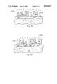
- FIGS. 1 and 2 are plan and cross-sectional views, respectively, of a conventional SOI MOS transistor.
- FIG. 3 is a plan view of an SOI MOS transistor constructed according to the invention, prior to silicidation.
- FIG. 4 is a cross-sectional view of the transistor of FIG. 3, subsequent to silicidation.
- FIGS. 5a through 5e are cross-sectional views illustrating the fabrication of p-channel and n-channel transistors according to the invention.
- FIG. 6 is a plan view of an SOI MOS transistor constructed according to a second embodiment of the invention.
- an n-channel SOI transistor according to the prior art is illustrated in plan view and cross-sectional view, respectively.
- the transistor is formed in a single-crystal silicon mesa 5 overlying an insulator film 4 which is formed on a silicon substrate 2.
- Insulator film 4 is generally silicon dioxide.
- the formation of mesa 5 over insulator 4 can be done by any one of a number of known methods such as SIMOX (Separation by IMplanted Oxygen), oxidized porous silicon (FIPOS), and thin film zone-melting recrystallization (ZMR).
- SIMOX Separation by IMplanted Oxygen
- FIPOS oxidized porous silicon
- ZMR thin film zone-melting recrystallization
- An example of the SIMOX process is described in application S.N. 035,126 filed April 7, 1987, and assigned to Texas Instruments Incorporated.
- Source region 6 and drain region 8 are heavily-doped n-type regions which are formed by ion implantation and subsequent diffusion.
- this example of a conventional transistor is formed according to the well-known lightly-doped drain construction, with implantation of the lightly-doped regions 18 performed in a self-aligned manner to gate electrode 10 (generally prior to formation of sidewall oxide filaments 16).
- FIGS. 1 and 2 are shown as formed in self-aligned fashion relative to the gate electrode 10 and sidewall oxide filaments 16, and fully extend from the surface of mesa 5 to the interface with insulator 4.
- Body node region 12 is a p-channel region which is not doped with n-type dopant used to form source and drain regions 6 and 8, but remains at the same conductivity type and concentration (p-type silicon which is lightly doped relative to the dopant concentration of source and drain regions 6 and 8) as originally formed.
- Sidewall filaments 23 passivate the edges of mesa 5.
- a refractory metal silicide film 22 such as titanium disilicide
- a refractory metal silicide film 22 is shown in FIG. 2 as cladding source and drain regions 6 and 8, as well as gate electrode 10.
- Such silicidation is useful in reducing the sheet resistance of the semiconducting layers, and is preferably done according to the well-known self-aligned direct react silicidation process, such as is described in U.S. Pat. No. 4,690,730 issued September 1, 1987, assigned to Texas Instruments Incorporated, and incorporated herein by this reference. Such silicidation is of course not essential to the operation of the transistor. Any one of the well known refractory metals conventionally used in silicidation, such as molybdenum, tungsten, and cobalt, may alternatively be used for formation of silicide film 22.
- body node 12 is electrically isolated in the transistor of FIGS. 1 and 2. Since source and drain regions 6 and 8 extend through the full thickness of mesa 5 to reach insulator 4, and since the self-alignment of source and drain regions 6 allows body node 12 to exist only under gate electrode 10 (and sidewall oxide filaments 14), it is inconvenient to form a contact to body node 12 in the structure of FIGS. 1 and 2. Accordingly, conventional SOI technology has the body node 12 of each MOS transistor in a floating state.
- the floating body node of the SOI transistor 1 presents certain problems in the performance, and performance stability, of the transistor.
- a first problem is the presence of a parasitic "back channel" transistor, having substrate 2 as a gate electrode and insulator film 4 as the gate dielectric. This back channel may provide for a drain-source leakage path along the body node 12 near the interface with insulator film 4, depending upon the local potential of substrate 2 at the transistor location.
- the voltage of body node 12 will affect the threshold voltage (V t ) of the transistor. While in bulk devices the MOS transistor body nodes are biased by the substrate, the dielectrically isolated body node 12 of transistor 1 of FIGS.
- 1 and 2 allows capacitive coupling between body node 12 and gate electrode 10, and diode coupling between body node 12 and source and drain regions 6 and 8, to bias body node 12 to an undesired potential. Furthermore, impact ionization occurs when carriers near the drain are at a sufficiently high potential that electron-hole pairs are created which, due to the minority carriers traveling to the source while the majority carriers travel to the drain, cause a voltage differential between body node 12 and source region 6, lowering the effective threshold voltage and increasing the drain current (i.e., the well known "kink" effect).
- Transistor 100 includes a contact between the source and body nodes to alleviate the problems of the floating body node described above relative to conventional transistor 1.
- the plan view of FIG. 3 shows p+contact regions 30 at the edge of the mesa, adjacent gate electrode 10 (and sidewall filaments 16).
- the conductive channel of transistor 100 remains along the edge of gate electrode 10 on the source side, between regions 30 at the edge. It should be noted that the view of FIG.
- silicide cladding is preferably used to connect source region 6 to p+contact regions 30 at the surface, and thus to provide the electrical connection from source region 30 to body node 12 underlying gate electrode 10.
- p+ contact regions 30 at the edge of the mesa 5 is not essential to provide for contact between the body node 12 and source region 6. However, as described in parent application S.N. 150,799, the presence of p+ contact regions 30 at the edge of the mesa reduces source-drain leakage of the transistor 100 in the event of exposure to ionizing radiation.
- the active semiconductor formed over the insulator layer 4 can, for many SOI technologies, contain a relatively large number of dislocation defects compared to the active region in bulk. These dislocations, especially along the edges of silicon mesas such as mesa 5, can allow diffused dopants forming source and drain regions 6 and 8 to diffuse through the body region 12, especially along the edges of mesa 5. This enhanced diffusion can cause short channel effects such as sub-threshold leakage in transistor 100 and, if the diffused dopant extends fully between source region 6 and drain region 8, can short drain region 8 to source region 6.
- the placement of the contact regions 30 at the edge of mesa 5 reduces the source/drain leakage resulting from such enhanced diffusion by separating the dopant of source region 6 from the edge of mesa 5 at gate electrode 10, so that enhanced diffusion into the body region 12 can come only from the drain side.
- placement of contact regions 30 at the edge of the mesa places a p+region between dopant from drain region 8 which diffuses through body region 12 along the edge of mesa 6, so that dopant reaching fully under gate electrode from drain region 8 will form only a reverse biased diode (contact region 30 being at the same potential as source region 6). Accordingly, the placement of contact regions 30 at the edge of mesa 5 reduces source/drain leakage due to such enhanced interfacial diffusion of the source/drain dopant.
- transistor 100 is shown in cross-section.
- source region 6 and drain region 8 extend through the full thickness of mesa 5, as does p+contact region 30. It should be noted that it is not essential for p+contact region 30 to so fully extend to insulator 4 in order to make contact to body node 12. It should be noted, however, that contact region 30 must extend sufficiently deeply to contact the body region which remains under the depletion layer below the channel of transistor 100 when conducting.
- FIG. 4 also illustrates the provision of silicide film 22 at the surface of the silicon structures (source region 6, p+contact region 30, drain region 8, and gate electrode 10). While ohmic connection may be made between p+contact region 30 and source region 6 by way of other interconnection means, such as conventional contacts through an overlying insulator film to a metallization layer, silicide film 22 provides a low resistance connection therebetween without an additional masking step.
- p+ contact region 30 includes a lightly-doped drain extension 38 which underlies the sidewall filament 16 on the side of gate electrode 10.
- Lightly-doped drain extension 38 is of course not essential to the formation of the contact to body node 12.
- the use of sidewall oxide filament 16 is preferred so that silicide film 22 on source and drain regions 6 and 8, respectively (as well as p+ contact region 30), are not electrically shorted to silicide film 22 on the surface of gate electrode 10.
- p+ contact region 30 can be doped as heavily as practicable in order to achieve the best contact to body node 12, without concern for drain-to-source junction breakdown through p+ region 30.
- Source and drain regions 6 and 8 generally can have an impurity concentration of 10 19 to 10 21 /cm 3 , with lightly-doped drain regions 18 and 38 in the range of 10 18 to 10 20 /cm 3 , depending upon the dopant gradient desired.
- FIGS. 5a through 5e the steps in the formation of an n-channel transistor 100n and an p-channel transistor 100p, as would be formed in a CMOS circuit, will be discussed to illustrate that the source-to-body contact according to the invention can be formed with no additional mask steps in a CMOS process.
- the cross-sectional views of FIGS. 5a through 5e are taken in a location analogous to that of FIG. 4, i.e., through the portion of the transistors 100 which will have the source-to-body contact.
- two mesas 5n and 5p are illustrated as formed overlying insulator layer 4; mesa 5n is n-type silicon and mesa 5p is p-type silicon.
- FIG. 5a illustrates a masking layer 40 overlying certain portions of the structures, and exposing portions thereof into which a p-type implant is to be made to form the lightly-doped drain extensions 18p for p-channel transistor 100p and extension 38p for the source-to-body contact in transistor 100n.
- Masking layer 40 may be patterned and developed photoresist or may be a hard mask layer, such as conventionally used for blocking ion implantation.
- the pattern of masking layer 40 is preferably designed so that masking layer 40 can overlap gate electrodes 10, and to overlap the edge of the mesas 5, for maximum alignment tolerance. As shown in FIG. 5a, the structure is exposed to a p-type implant of boron of another p-type dopant, to form the lightly-doped drain extensions 18 and 38, using conventional doses and energies for such an implant.
- FIG. 5b the structure is shown after the implantation of FIG. 5a, and after the formation of masking layer 42 which is to protect the regions into which the p-type implant of FIG. 5a has been made and to expose the regions of the structures into which the n-type lightly-doped drain implant is to be made.
- FIG. 5b shows lightly-doped drain extensions 18p and 38p are driven approximately to their final depth. It should be noted that each of the implants shown in FIGS. 5a through 5b may not be driven immediately after each masking step, but that a single drive-in anneal may be done after all four of the implants described herein are performed.
- FIG. 5b illustrates the structures as receiving the n-type (arsenic, phosphorous, or other conventional dopants) lightly-doped drain implant, in conventional doses and energies.
- transistors 100n and 100p are shown at the point of receiving the heavy p-type source/drain implant.
- Sidewall oxide filaments 16 are in place adjacent the sides of gate electrodes 10, to protect a portion of region 18p in transistor 100p, and to protect region 38p in transistor 1OOn, from the heavy source/drain implant so that a graded junction will result as is well known in the art.
- Sidewall oxide filaments 16 are formed by way of deposition of an oxide layer, such as by decomposition of TEOS, followed by an anisotropic etch of the oxide to leave the sidewall filaments 16 behind.
- Mask layer 50 is formed to protect the n-type implanted regions 18n and 38n from the p-type source/drain implant, and to expose the p-type implanted regions (except as protected by filaments 16) thereto. It should be noted that the pattern used to form mask layer 50 may be identical to the pattern used to form mask layer 40.
- the p-type source/drain implant is then performed, as illustrated in FIG. 5c, according to conventional doses and energies for such an implant.
- FIG. 5d illustrates the presence of source region 6p and drain region 8p in transistor 100p, and the presence of p+ contact region 30p in transistor 100n for contact to the body node of transistor 100n. Also shown in FIG. 5d is the final source/drain pattern mask layer 52 for protecting the p+ regions 6p, 8p and 30p from the n-type source/drain implant, and for exposing the regions of transistors 100n and 100p that are to receive the implant.
- the implant of FIG. 5d will thus eventually form the source and drain regions 6 and 8, respectively, of transistor 100n, and will also form an n+ contact region for contact between source region 6p and the body node of transistor 100n, analogous to the p+ contact region 30 in transistor 100 shown in FIGS. 3 and 4.
- FIG. 5e The result of the implant of FIG. 5d, after the drive-in anneal, is shown in FIG. 5e.
- Source region 6n and drain region 6n are formed in transistor 100n, similarly as shown in FIG. 4.
- n+ contact region 30n having lightly-doped drain extension 38n, is present to make contact between source region 6p and body node 12n of transistor 100n.
- the structure of FIG. 5e is then subjected to the direct react silicidation process, as described hereinabove, to result in the ohmic connection between the source nodes 6p and 6n to body nodes 12n and 12p, respectively, through the respective contact regions 30n and 30p.
- FIG. 6 illustrates, in plan view, a transistor 200 constructed according to a second embodiment of the invention.
- Transistor 200 similarly as transistor 100 in FIG. 3, is shown prior to the silicidation for connecting p+ contact regions 30 to source region 6.
- Transistor 200 has multiple p+ contact regions 30, placed not only at the edge of mesa 5, but also in the interior of transistor 200.
- body node 12 may not receive a uniform bias from source region 6 through p+ contact region 30 over such a relatively long width due to its relatively light doping concentration. Accordingly, the interior ones of p+ contact regions 30 are provided to more uniformly bias the entire width of the underlying body node 12.
- Characterization of transistors fabricated according to a given set of process parameters and geometries may indicate that contact regions 30 must be spaced apart mo greated than a certain distance to provide such constant bias. This may then result in contact regions 30 spaced apart by no more than a particular distance, although the spacing of such plural contact regions 30 may not necessarily be uniform as suggested by FIG. 6.
- a single contact region 30, at one edge of source region 6, may be sufficient to bias the body node 12 uniformly. Since each contact region 30 reduces the effective channel width of the transistor, it is preferable to minimize the number and size of contact regions 30 to the minimum necessary to provide sufficiently uniform bias to body node 12.
- the contact regions 30 provided according to the invention do not require additional patterning in the formation of the mesas 5 or the gate electrodes 10 except for the masks used during the implant steps. Accordingly, it is not necessary to specify which side of the transistor is to be the source and which is to be the drain until the implant steps are performed.
- the instant invention is thus particularly advantageous in the formation of transistors in gate arrays and other mask-programmable logic, as the masks used to form the mesas 5 and gates 10 may be common to all devices fabricated with the same process, with the personalization of the gate array (and specification of source and drain) done by way of the implant masks.
- such devices may include transistors to which body node contact is not desired, such as a pass transistor; for which case the contact regions 30 may be precluded using the same implant mask levels.
Abstract
Description
Claims (6)
Priority Applications (2)
| Application Number | Priority Date | Filing Date | Title |
|---|---|---|---|
| US07/216,932 US4965213A (en) | 1988-02-01 | 1988-07-08 | Silicon-on-insulator transistor with body node to source node connection |
| JP17539789A JPH02148865A (en) | 1988-07-08 | 1989-07-06 | Silicon transistor on insulator including connection between body node and source node |
Applications Claiming Priority (2)
| Application Number | Priority Date | Filing Date | Title |
|---|---|---|---|
| US07/150,799 US4974051A (en) | 1988-02-01 | 1988-02-01 | MOS transistor with improved radiation hardness |
| US07/216,932 US4965213A (en) | 1988-02-01 | 1988-07-08 | Silicon-on-insulator transistor with body node to source node connection |
Related Parent Applications (1)
| Application Number | Title | Priority Date | Filing Date |
|---|---|---|---|
| US07/150,799 Continuation-In-Part US4974051A (en) | 1988-02-01 | 1988-02-01 | MOS transistor with improved radiation hardness |
Publications (1)
| Publication Number | Publication Date |
|---|---|
| US4965213A true US4965213A (en) | 1990-10-23 |
Family
ID=26848051
Family Applications (1)
| Application Number | Title | Priority Date | Filing Date |
|---|---|---|---|
| US07/216,932 Expired - Fee Related US4965213A (en) | 1988-02-01 | 1988-07-08 | Silicon-on-insulator transistor with body node to source node connection |
Country Status (1)
| Country | Link |
|---|---|
| US (1) | US4965213A (en) |
Cited By (50)
| Publication number | Priority date | Publication date | Assignee | Title |
|---|---|---|---|---|
| US5026656A (en) * | 1988-02-01 | 1991-06-25 | Texas Instruments Incorporated | MOS transistor with improved radiation hardness |
| US5066613A (en) * | 1989-07-13 | 1991-11-19 | The United States Of America As Represented By The Secretary Of The Navy | Process for making semiconductor-on-insulator device interconnects |
| US5185280A (en) * | 1991-01-29 | 1993-02-09 | Texas Instruments Incorporated | Method of fabricating a soi transistor with pocket implant and body-to-source (bts) contact |
| US5225356A (en) * | 1991-01-14 | 1993-07-06 | Nippon Telegraph & Telephone Corporation | Method of making field-effect semiconductor device on sot |
| US5300448A (en) * | 1991-02-01 | 1994-04-05 | North American Philips Corporation | High voltage thin film transistor having a linear doping profile and method for making |
| US5344785A (en) * | 1992-03-13 | 1994-09-06 | United Technologies Corporation | Method of forming high speed, high voltage fully isolated bipolar transistors on a SOI substrate |
| US5360752A (en) * | 1993-10-28 | 1994-11-01 | Loral Federal Systems Company | Method to radiation harden the buried oxide in silicon-on-insulator structures |
| USH1435H (en) * | 1991-10-21 | 1995-05-02 | Cherne Richard D | SOI CMOS device having body extension for providing sidewall channel stop and bodytie |
| US5482870A (en) * | 1990-06-08 | 1996-01-09 | Seiko Epson Corporation | Methods for manufacturing low leakage current offset-gate thin film transistor |
| US5518940A (en) * | 1994-03-10 | 1996-05-21 | Fujitsu Limited | Method of manufacturing thin film transistors in a liquid crystal display |
| US5580804A (en) * | 1994-12-15 | 1996-12-03 | Advanced Micro Devices, Inc. | Method for fabricating true LDD devices in a MOS technology |
| US5595944A (en) * | 1993-03-12 | 1997-01-21 | Semiconductor Energy Laboratory Co., Inc. | Transistor and process for fabricating the same |
| US5635744A (en) * | 1994-09-08 | 1997-06-03 | Mitsubushi Denki Kabushiki Kaisha | Semiconductor memory and semiconductor device having SOI structure |
| US5683918A (en) * | 1996-04-01 | 1997-11-04 | Motorola, Inc. | Method of making semiconductor-on-insulator device with closed-gate electrode |
| US5804858A (en) * | 1995-06-08 | 1998-09-08 | Taiwan Semiconductor Manufacturing, Ltd. | Body contacted SOI MOSFET |
| US5825696A (en) * | 1993-12-03 | 1998-10-20 | Mitsubishi Denki Kabushiki Kaisha | Semiconductor memory device including an SOI substrate |
| EP0902482A1 (en) * | 1997-09-05 | 1999-03-17 | Sharp Kabushiki Kaisha | SOI-MOSFET and fabrication process thereof |
| US5915197A (en) * | 1993-10-07 | 1999-06-22 | Nec Corporation | Fabrication process for semiconductor device |
| US5936278A (en) * | 1996-03-13 | 1999-08-10 | Texas Instruments Incorporated | Semiconductor on silicon (SOI) transistor with a halo implant |
| US5982005A (en) * | 1995-02-17 | 1999-11-09 | Mitsubishi Denki Kabushiki Kaisha | Semiconductor device using an SOI substrate |
| US6018172A (en) * | 1994-09-26 | 2000-01-25 | Mitsubishi Denki Kabushiki Kaisha | Semiconductor memory device including memory cell transistors formed on SOI substrate and having fixed body regions |
| US6060900A (en) * | 1998-06-30 | 2000-05-09 | United Semicondutor Circuit Corp. | Method for measuring current density in a semiconductor device with kink effect |
| US6180983B1 (en) | 1998-07-17 | 2001-01-30 | National Semiconductor Corporation | High-voltage MOS transistor on a silicon on insulator wafer |
| WO2001050516A1 (en) * | 2000-01-07 | 2001-07-12 | Seiko Epson Corporation | Method of manufacturing a thin-film transistor |
| US6261875B1 (en) | 1993-03-12 | 2001-07-17 | Semiconductor Energy Laboratory Co., Ltd. | Transistor and process for fabricating the same |
| US6337500B1 (en) * | 1997-06-19 | 2002-01-08 | Matsushita Electric Industrial Co., Ltd. | Semiconductor device and method for fabricating the same |
| US6339005B1 (en) | 1999-10-22 | 2002-01-15 | International Business Machines Corporation | Disposable spacer for symmetric and asymmetric Schottky contact to SOI MOSFET |
| US6353245B1 (en) | 1998-04-09 | 2002-03-05 | Texas Instruments Incorporated | Body-tied-to-source partially depleted SOI MOSFET |
| US6368903B1 (en) * | 2000-03-17 | 2002-04-09 | International Business Machines Corporation | SOI low capacitance body contact |
| US6383850B2 (en) * | 1999-01-11 | 2002-05-07 | Mitsubishi Denki Kabushiki Kaisha | Semiconductor device and method of manufacturing the same |
| US6399989B1 (en) | 1999-08-03 | 2002-06-04 | Bae Systems Information And Electronic Systems Integration Inc. | Radiation hardened silicon-on-insulator (SOI) transistor having a body contact |
| US6455875B2 (en) | 1992-10-09 | 2002-09-24 | Semiconductor Energy Laboratory Co., Ltd. | Thin film transistor having enhanced field mobility |
| US6507069B1 (en) | 1994-07-14 | 2003-01-14 | Semiconductor Energy Laboratory Co., Ltd. | Semiconductor device and method of manufacture thereof |
| US20030025159A1 (en) * | 2001-06-27 | 2003-02-06 | Michiru Hogyoku | Semiconductor devices |
| US6555446B1 (en) * | 1999-12-10 | 2003-04-29 | Texas Instruments Incorporated | Body contact silicon-on-insulator transistor and method |
| US6596615B2 (en) * | 1996-04-24 | 2003-07-22 | Mitsubishi Denki Kabushiki Kaisha | Semiconductor device and method of manufacturing the same |
| US6624477B1 (en) | 1992-10-09 | 2003-09-23 | Semiconductor Energy Laboratory Co., Ltd. | Semiconductor device and method for manufacturing the same |
| US20030217620A1 (en) * | 2002-04-08 | 2003-11-27 | Council Scientific And Industrial Research | Process for the production of neodymium-iron-boron permanent magnet alloy powder |
| US20030222308A1 (en) * | 2002-05-30 | 2003-12-04 | Taiwan Semiconductor Manufacturing Co., Ltd. | SOI MOSFET with compact body-tied-source structure |
| US6677645B2 (en) | 2002-01-31 | 2004-01-13 | International Business Machines Corporation | Body contact MOSFET |
| US6716728B2 (en) | 1999-08-03 | 2004-04-06 | Bae Systems Information And Electronic Systems Integration, Inc. | Radiation hardened silicon-on-insulator (SOI) transistor having a body contact |
| US6906383B1 (en) | 1994-07-14 | 2005-06-14 | Semiconductor Energy Laboratory Co., Ltd. | Semiconductor device and method of manufacture thereof |
| US20050269600A1 (en) * | 2002-09-27 | 2005-12-08 | Infineon Technologies Ag | Integrated field-effect transistor comprising two control regions, use of said field-effect transistor and method for producing the same |
| US20060157788A1 (en) * | 2005-01-19 | 2006-07-20 | International Business Machines Corporation | SRAM memories and microprocessors having logic portions implemented in high-performance silicon substrates and SRAM array portions having field effect transistors with linked bodies and methods for making same |
| US20080237708A1 (en) * | 2007-03-26 | 2008-10-02 | International Business Machines Corporation | SILICON ON INSULATOR (SOI) FIELD EFFECT TRANSISTORS (FETs) WITH ADJACENT BODY CONTACTS |
| US20100099227A1 (en) * | 1996-07-11 | 2010-04-22 | Semiconductor Energy Laboratory Co., Ltd. | Semiconductor device and method of manufacturing the same |
| US20100155842A1 (en) * | 2008-12-23 | 2010-06-24 | International Business Machines Corporation | Body contacted hybrid surface semiconductor-on-insulator devices |
| US20120164801A1 (en) * | 1996-07-11 | 2012-06-28 | Semiconductor Energy Laboratory Co., Ltd. | Semiconductor device and method of manufacturing the same |
| US9177968B1 (en) | 2014-09-19 | 2015-11-03 | Silanna Semiconductor U.S.A., Inc. | Schottky clamped radio frequency switch |
| WO2019203938A1 (en) * | 2018-04-20 | 2019-10-24 | Qualcomm Incorporated | Body connection for a silicon-on-insulator device |
Citations (3)
| Publication number | Priority date | Publication date | Assignee | Title |
|---|---|---|---|---|
| US4053916A (en) * | 1975-09-04 | 1977-10-11 | Westinghouse Electric Corporation | Silicon on sapphire MOS transistor |
| US4753896A (en) * | 1986-11-21 | 1988-06-28 | Texas Instruments Incorporated | Sidewall channel stop process |
| US4906587A (en) * | 1988-07-29 | 1990-03-06 | Texas Instruments Incorporated | Making a silicon-on-insulator transistor with selectable body node to source node connection |
-
1988
- 1988-07-08 US US07/216,932 patent/US4965213A/en not_active Expired - Fee Related
Patent Citations (4)
| Publication number | Priority date | Publication date | Assignee | Title |
|---|---|---|---|---|
| US4053916A (en) * | 1975-09-04 | 1977-10-11 | Westinghouse Electric Corporation | Silicon on sapphire MOS transistor |
| US4053916B1 (en) * | 1975-09-04 | 1983-03-08 | ||
| US4753896A (en) * | 1986-11-21 | 1988-06-28 | Texas Instruments Incorporated | Sidewall channel stop process |
| US4906587A (en) * | 1988-07-29 | 1990-03-06 | Texas Instruments Incorporated | Making a silicon-on-insulator transistor with selectable body node to source node connection |
Non-Patent Citations (8)
| Title |
|---|
| Kumamoto et al., "An SOI Structure for Flash A/D Converter", IEEE Journal of Solid-State Circuits, vol. 23, No. 1, (Feb. 1988), pp. 198-201. |
| Kumamoto et al., An SOI Structure for Flash A/D Converter , IEEE Journal of Solid State Circuits, vol. 23, No. 1, (Feb. 1988), pp. 198 201. * |
| Lee et al., "Island-Edge Effects in C-MOS/SOS Transistors", IEEE Transactions on Electron Devices, vol. Ed-25, No. 8, Aug. 1978, pp. 971-978. |
| Lee et al., Island Edge Effects in C MOS/SOS Transistors , IEEE Transactions on Electron Devices, vol. Ed 25, No. 8, Aug. 1978, pp. 971 978. * |
| Tihanyi et al., "Influence of the Floating Substrate Potential on the Characteristics of ESFI MOS Transistors", Solid State Electronics, 1975, (Pergamon), vol. 18, pp. 309-314. |
| Tihanyi et al., "Properties of ESFI MOS Transistors Due to the Floating Substrate and the Finite Volume", IEEE Trans. on Electron Devices, vol. ED-22, No. 11, (Nov. 1975), pp. 1017-1023. |
| Tihanyi et al., Influence of the Floating Substrate Potential on the Characteristics of ESFI MOS Transistors , Solid State Electronics, 1975, (Pergamon), vol. 18, pp. 309 314. * |
| Tihanyi et al., Properties of ESFI MOS Transistors Due to the Floating Substrate and the Finite Volume , IEEE Trans. on Electron Devices, vol. ED 22, No. 11, (Nov. 1975), pp. 1017 1023. * |
Cited By (110)
| Publication number | Priority date | Publication date | Assignee | Title |
|---|---|---|---|---|
| US5026656A (en) * | 1988-02-01 | 1991-06-25 | Texas Instruments Incorporated | MOS transistor with improved radiation hardness |
| US5066613A (en) * | 1989-07-13 | 1991-11-19 | The United States Of America As Represented By The Secretary Of The Navy | Process for making semiconductor-on-insulator device interconnects |
| US5482870A (en) * | 1990-06-08 | 1996-01-09 | Seiko Epson Corporation | Methods for manufacturing low leakage current offset-gate thin film transistor |
| US5225356A (en) * | 1991-01-14 | 1993-07-06 | Nippon Telegraph & Telephone Corporation | Method of making field-effect semiconductor device on sot |
| US5185280A (en) * | 1991-01-29 | 1993-02-09 | Texas Instruments Incorporated | Method of fabricating a soi transistor with pocket implant and body-to-source (bts) contact |
| US5300448A (en) * | 1991-02-01 | 1994-04-05 | North American Philips Corporation | High voltage thin film transistor having a linear doping profile and method for making |
| USH1435H (en) * | 1991-10-21 | 1995-05-02 | Cherne Richard D | SOI CMOS device having body extension for providing sidewall channel stop and bodytie |
| US5344785A (en) * | 1992-03-13 | 1994-09-06 | United Technologies Corporation | Method of forming high speed, high voltage fully isolated bipolar transistors on a SOI substrate |
| US7723788B2 (en) | 1992-10-09 | 2010-05-25 | Semiconductor Energy Laboratory Co., Ltd. | Semiconductor device and method for forming the same |
| US20090152631A1 (en) * | 1992-10-09 | 2009-06-18 | Semiconductor Energy Laboratory Co., Ltd. | Semiconductor device and method for forming the same |
| US8017506B2 (en) | 1992-10-09 | 2011-09-13 | Semiconductor Energy Laboratory Co., Ltd. | Semiconductor device and method for forming the same |
| US20030006414A1 (en) * | 1992-10-09 | 2003-01-09 | Semiconductor Energy Laboratory Co., Ltd. | Semiconductor device and method for forming the same |
| US7109108B2 (en) | 1992-10-09 | 2006-09-19 | Semiconductor Energy Laboratory Co., Ltd. | Method for manufacturing semiconductor device having metal silicide |
| US20100041187A1 (en) * | 1992-10-09 | 2010-02-18 | Semiconductor Energy Laboratory Co., Ltd. | Semiconductor device and method for forming the same |
| US7602020B2 (en) | 1992-10-09 | 2009-10-13 | Semiconductor Energy Laboratory Co., Ltd. | Semiconductor device and method for forming the same |
| US20050037549A1 (en) * | 1992-10-09 | 2005-02-17 | Semiconductor Energy Laboratory Co., Ltd. | Semiconductor device and method for forming the same |
| US6624477B1 (en) | 1992-10-09 | 2003-09-23 | Semiconductor Energy Laboratory Co., Ltd. | Semiconductor device and method for manufacturing the same |
| US6790749B2 (en) | 1992-10-09 | 2004-09-14 | Semiconductor Energy Laboratory Co., Ltd. | Method of manufacturing a semiconductor device |
| US6455875B2 (en) | 1992-10-09 | 2002-09-24 | Semiconductor Energy Laboratory Co., Ltd. | Thin film transistor having enhanced field mobility |
| US6541313B2 (en) | 1993-03-12 | 2003-04-01 | Semiconductor Energy Laboratory Co., Ltd. | Transistor and process for fabricating the same |
| US5595944A (en) * | 1993-03-12 | 1997-01-21 | Semiconductor Energy Laboratory Co., Inc. | Transistor and process for fabricating the same |
| US6939749B2 (en) | 1993-03-12 | 2005-09-06 | Semiconductor Energy Laboratory Co., Ltd | Method of manufacturing a semiconductor device that includes heating the gate insulating film |
| US6060725A (en) * | 1993-03-12 | 2000-05-09 | Semiconductor Energy Laboratory Co., Ltd. | Thin film transistor using a semiconductor film |
| US6261875B1 (en) | 1993-03-12 | 2001-07-17 | Semiconductor Energy Laboratory Co., Ltd. | Transistor and process for fabricating the same |
| US5915197A (en) * | 1993-10-07 | 1999-06-22 | Nec Corporation | Fabrication process for semiconductor device |
| US5360752A (en) * | 1993-10-28 | 1994-11-01 | Loral Federal Systems Company | Method to radiation harden the buried oxide in silicon-on-insulator structures |
| US20050001254A1 (en) * | 1993-12-03 | 2005-01-06 | Renesas Technology Corp. | Semiconductor memory device including an SOI substrate |
| US7138684B2 (en) | 1993-12-03 | 2006-11-21 | Renesas Technology Corp. | Semiconductor memory device including an SOI substrate |
| US6288949B1 (en) | 1993-12-03 | 2001-09-11 | Mitsubishi Denki Kabushiki Kaisha | Semiconductor memory device including an SOI substrate |
| US20070052028A1 (en) * | 1993-12-03 | 2007-03-08 | Renesas Technology Corp. | Semiconductor memory device including an SOI substrate |
| US7242060B2 (en) | 1993-12-03 | 2007-07-10 | Renesas Technology Corp. | Semiconductor memory device including an SOI substrate |
| US6091647A (en) * | 1993-12-03 | 2000-07-18 | Mitsubishi Denki Kabushiki Kaisha | Semiconductor memory device including an SOI substrate |
| US20070257313A1 (en) * | 1993-12-03 | 2007-11-08 | Renesas Technology Corp. | Semiconductor memory device including an SOI substrate |
| US6768662B2 (en) | 1993-12-03 | 2004-07-27 | Renesas Technology Corp. | Semiconductor memory device including an SOI substrate |
| US5825696A (en) * | 1993-12-03 | 1998-10-20 | Mitsubishi Denki Kabushiki Kaisha | Semiconductor memory device including an SOI substrate |
| US6385159B2 (en) | 1993-12-03 | 2002-05-07 | Mitsubishi Denki Kabushiki Kaisha | Semiconductor memory device including an SOI substrate |
| US6577522B2 (en) | 1993-12-03 | 2003-06-10 | Mitsubishi Denki Kabushiki Kaisha | Semiconductor memory device including an SOI substrate |
| US20060118849A1 (en) * | 1993-12-03 | 2006-06-08 | Hideto Hidaka | Semiconductor memory device including an SOI |
| US5518940A (en) * | 1994-03-10 | 1996-05-21 | Fujitsu Limited | Method of manufacturing thin film transistors in a liquid crystal display |
| US20070138473A1 (en) * | 1994-07-14 | 2007-06-21 | Semiconductor Energy Laboratory Co., Ltd. | Semiconductor device and method of manufacture thereof |
| US6906383B1 (en) | 1994-07-14 | 2005-06-14 | Semiconductor Energy Laboratory Co., Ltd. | Semiconductor device and method of manufacture thereof |
| US6507069B1 (en) | 1994-07-14 | 2003-01-14 | Semiconductor Energy Laboratory Co., Ltd. | Semiconductor device and method of manufacture thereof |
| US20100068860A1 (en) * | 1994-07-14 | 2010-03-18 | Semiconductor Energy Laboratory Co., Ltd. | Semiconductor device and method of manufacture thereof |
| US6773971B1 (en) | 1994-07-14 | 2004-08-10 | Semiconductor Energy Laboratory Co., Ltd. | Method of manufacturing a semiconductor device having lightly-doped drain (LDD) regions |
| US7635895B2 (en) | 1994-07-14 | 2009-12-22 | Semiconductor Energy Laboratory Co., Ltd. | Display device |
| US7183614B2 (en) | 1994-07-14 | 2007-02-27 | Semiconductor Energy Laboratory Co., Ltd. | Semiconductor device and method of manufacture thereof |
| US8273613B2 (en) | 1994-07-14 | 2012-09-25 | Semiconductor Energy Laboratory Co., Ltd. | Semiconductor device and method of manufacture thereof |
| US20050224796A1 (en) * | 1994-07-14 | 2005-10-13 | Semiconductor Energy Laboratory Co., Ltd. | Semiconductor device and method of manufacture thereof |
| US5635744A (en) * | 1994-09-08 | 1997-06-03 | Mitsubushi Denki Kabushiki Kaisha | Semiconductor memory and semiconductor device having SOI structure |
| US5773865A (en) * | 1994-09-08 | 1998-06-30 | Mitsubishi Denki Kabushiki Kaisha | Semiconductor memory and semiconductor device having SOI structure |
| US6384445B1 (en) | 1994-09-26 | 2002-05-07 | Mitsubishi Denki Kabushiki Kaisha | Semiconductor memory device including memory cell transistors formed on SOI substrate and having fixed body regions |
| US6018172A (en) * | 1994-09-26 | 2000-01-25 | Mitsubishi Denki Kabushiki Kaisha | Semiconductor memory device including memory cell transistors formed on SOI substrate and having fixed body regions |
| US5580804A (en) * | 1994-12-15 | 1996-12-03 | Advanced Micro Devices, Inc. | Method for fabricating true LDD devices in a MOS technology |
| US6586803B2 (en) | 1995-02-17 | 2003-07-01 | Mitsubishi Denki Kabushiki Kaisha | Semiconductor device using an SOI substrate |
| US20040067614A1 (en) * | 1995-02-17 | 2004-04-08 | Mitsubishi Denki Kabushiki Kaisha | Semiconductor device using an SOI substrate |
| US5982005A (en) * | 1995-02-17 | 1999-11-09 | Mitsubishi Denki Kabushiki Kaisha | Semiconductor device using an SOI substrate |
| US6787853B2 (en) | 1995-02-17 | 2004-09-07 | Renesas Technology Corp. | Semiconductor device using an SOI substrate |
| US5804858A (en) * | 1995-06-08 | 1998-09-08 | Taiwan Semiconductor Manufacturing, Ltd. | Body contacted SOI MOSFET |
| US5936278A (en) * | 1996-03-13 | 1999-08-10 | Texas Instruments Incorporated | Semiconductor on silicon (SOI) transistor with a halo implant |
| US5683918A (en) * | 1996-04-01 | 1997-11-04 | Motorola, Inc. | Method of making semiconductor-on-insulator device with closed-gate electrode |
| US6596615B2 (en) * | 1996-04-24 | 2003-07-22 | Mitsubishi Denki Kabushiki Kaisha | Semiconductor device and method of manufacturing the same |
| US6818536B2 (en) | 1996-04-24 | 2004-11-16 | Renesas Technology Corp. | Semiconductor device and method of manufacturing the same |
| US8129232B2 (en) * | 1996-07-11 | 2012-03-06 | Semiconductor Energy Laboratory Co., Ltd. | Semiconductor device and method of manufacturing the same |
| US20120164801A1 (en) * | 1996-07-11 | 2012-06-28 | Semiconductor Energy Laboratory Co., Ltd. | Semiconductor device and method of manufacturing the same |
| US20100099227A1 (en) * | 1996-07-11 | 2010-04-22 | Semiconductor Energy Laboratory Co., Ltd. | Semiconductor device and method of manufacturing the same |
| US8603870B2 (en) * | 1996-07-11 | 2013-12-10 | Semiconductor Energy Laboratory Co., Ltd. | Semiconductor device and method of manufacturing the same |
| US6770517B2 (en) | 1997-06-19 | 2004-08-03 | Matsushita Electric Industrial Co., Ltd. | Semiconductor device and method for fabricating the same |
| US6337500B1 (en) * | 1997-06-19 | 2002-01-08 | Matsushita Electric Industrial Co., Ltd. | Semiconductor device and method for fabricating the same |
| US20020058361A1 (en) * | 1997-06-19 | 2002-05-16 | Matsushita Electric Industrial Co., Ltd. | Semiconductor device and method for fabricating the same |
| US6288425B1 (en) | 1997-09-05 | 2001-09-11 | Sharp Kabushiki Kaisha | SOI-MOSFET device |
| EP0902482A1 (en) * | 1997-09-05 | 1999-03-17 | Sharp Kabushiki Kaisha | SOI-MOSFET and fabrication process thereof |
| US6353245B1 (en) | 1998-04-09 | 2002-03-05 | Texas Instruments Incorporated | Body-tied-to-source partially depleted SOI MOSFET |
| US6060900A (en) * | 1998-06-30 | 2000-05-09 | United Semicondutor Circuit Corp. | Method for measuring current density in a semiconductor device with kink effect |
| US6180983B1 (en) | 1998-07-17 | 2001-01-30 | National Semiconductor Corporation | High-voltage MOS transistor on a silicon on insulator wafer |
| US6383850B2 (en) * | 1999-01-11 | 2002-05-07 | Mitsubishi Denki Kabushiki Kaisha | Semiconductor device and method of manufacturing the same |
| US6716728B2 (en) | 1999-08-03 | 2004-04-06 | Bae Systems Information And Electronic Systems Integration, Inc. | Radiation hardened silicon-on-insulator (SOI) transistor having a body contact |
| US6399989B1 (en) | 1999-08-03 | 2002-06-04 | Bae Systems Information And Electronic Systems Integration Inc. | Radiation hardened silicon-on-insulator (SOI) transistor having a body contact |
| US6596554B2 (en) * | 1999-09-02 | 2003-07-22 | Texas Instruments Incorporated | Body-tied-to-source partially depleted SOI MOSFET |
| US7183573B2 (en) | 1999-10-22 | 2007-02-27 | International Business Machines Corporation | Disposable spacer for symmetric and asymmetric Schottky contact to SOI mosfet |
| US6339005B1 (en) | 1999-10-22 | 2002-01-15 | International Business Machines Corporation | Disposable spacer for symmetric and asymmetric Schottky contact to SOI MOSFET |
| US6724047B2 (en) | 1999-12-10 | 2004-04-20 | Texas Instruments Incorporated | Body contact silicon-on-insulator transistor and method |
| US6555446B1 (en) * | 1999-12-10 | 2003-04-29 | Texas Instruments Incorporated | Body contact silicon-on-insulator transistor and method |
| US6727123B2 (en) * | 2000-01-07 | 2004-04-27 | Seiko Epson Corporation | Method for manufacturing a thin-film transistor comprising a recombination center |
| WO2001050516A1 (en) * | 2000-01-07 | 2001-07-12 | Seiko Epson Corporation | Method of manufacturing a thin-film transistor |
| US6624475B2 (en) | 2000-03-17 | 2003-09-23 | International Business Machines Corporation | SOI low capacitance body contact |
| US6368903B1 (en) * | 2000-03-17 | 2002-04-09 | International Business Machines Corporation | SOI low capacitance body contact |
| US6835982B2 (en) * | 2001-06-27 | 2004-12-28 | Seiko Epson Corporation | Semiconductor devices |
| US20030025159A1 (en) * | 2001-06-27 | 2003-02-06 | Michiru Hogyoku | Semiconductor devices |
| US6677645B2 (en) | 2002-01-31 | 2004-01-13 | International Business Machines Corporation | Body contact MOSFET |
| US20040079995A1 (en) * | 2002-01-31 | 2004-04-29 | Andres Bryant | Body contact mosfet |
| US6940130B2 (en) | 2002-01-31 | 2005-09-06 | International Business Machines Corporation | Body contact MOSFET |
| US20030217620A1 (en) * | 2002-04-08 | 2003-11-27 | Council Scientific And Industrial Research | Process for the production of neodymium-iron-boron permanent magnet alloy powder |
| US20030222308A1 (en) * | 2002-05-30 | 2003-12-04 | Taiwan Semiconductor Manufacturing Co., Ltd. | SOI MOSFET with compact body-tied-source structure |
| US20050269600A1 (en) * | 2002-09-27 | 2005-12-08 | Infineon Technologies Ag | Integrated field-effect transistor comprising two control regions, use of said field-effect transistor and method for producing the same |
| US8518759B2 (en) | 2002-09-27 | 2013-08-27 | Infineon Technologies Ag | Method for producing an integrated field-effect transistor |
| US20100317162A1 (en) * | 2002-09-27 | 2010-12-16 | Infineon Technologies Ag | Method for producing an integrated field-effect transistor |
| US7960789B2 (en) | 2002-09-27 | 2011-06-14 | Infineon Technologies Ag | Integrated field-effect transistor comprising two control regions, use of said field-effect transistor and method for producing the same |
| US20060157788A1 (en) * | 2005-01-19 | 2006-07-20 | International Business Machines Corporation | SRAM memories and microprocessors having logic portions implemented in high-performance silicon substrates and SRAM array portions having field effect transistors with linked bodies and methods for making same |
| US7217978B2 (en) * | 2005-01-19 | 2007-05-15 | International Business Machines Corporation | SRAM memories and microprocessors having logic portions implemented in high-performance silicon substrates and SRAM array portions having field effect transistors with linked bodies and method for making same |
| US8587062B2 (en) | 2007-03-26 | 2013-11-19 | International Business Machines Corporation | Silicon on insulator (SOI) field effect transistors (FETs) with adjacent body contacts |
| US20080237708A1 (en) * | 2007-03-26 | 2008-10-02 | International Business Machines Corporation | SILICON ON INSULATOR (SOI) FIELD EFFECT TRANSISTORS (FETs) WITH ADJACENT BODY CONTACTS |
| US8227867B2 (en) * | 2008-12-23 | 2012-07-24 | International Business Machines Corporation | Body contacted hybrid surface semiconductor-on-insulator devices |
| US20100155842A1 (en) * | 2008-12-23 | 2010-06-24 | International Business Machines Corporation | Body contacted hybrid surface semiconductor-on-insulator devices |
| US8962398B2 (en) | 2008-12-23 | 2015-02-24 | International Business Machines Corporation | Body contacted hybrid surface semiconductor-on-insulator devices |
| US9023694B2 (en) | 2008-12-23 | 2015-05-05 | International Business Machines Corporation | Body contacted hybrid surface semiconductor-on-insulator devices |
| US9177968B1 (en) | 2014-09-19 | 2015-11-03 | Silanna Semiconductor U.S.A., Inc. | Schottky clamped radio frequency switch |
| US9502433B2 (en) | 2014-09-19 | 2016-11-22 | Qualcomm Incorporated | Schottky clamped radio frequency switch |
| WO2019203938A1 (en) * | 2018-04-20 | 2019-10-24 | Qualcomm Incorporated | Body connection for a silicon-on-insulator device |
| US20190326401A1 (en) * | 2018-04-20 | 2019-10-24 | Qualcomm Incorporated | Body connection for a silicon-on-insulator device |
| CN111989781A (en) * | 2018-04-20 | 2020-11-24 | 高通股份有限公司 | Body connection for silicon-on-insulator devices |
Similar Documents
| Publication | Publication Date | Title |
|---|---|---|
| US4965213A (en) | Silicon-on-insulator transistor with body node to source node connection | |
| US4946799A (en) | Process for making high performance silicon-on-insulator transistor with body node to source node connection | |
| US4899202A (en) | High performance silicon-on-insulator transistor with body node to source node connection | |
| US5144390A (en) | Silicon-on insulator transistor with internal body node to source node connection | |
| US4906587A (en) | Making a silicon-on-insulator transistor with selectable body node to source node connection | |
| US5359219A (en) | Silicon on insulator device comprising improved substrate doping | |
| US5185280A (en) | Method of fabricating a soi transistor with pocket implant and body-to-source (bts) contact | |
| US5438007A (en) | Method of fabricating field effect transistor having polycrystalline silicon gate junction | |
| US7382024B2 (en) | Low threshold voltage PMOS apparatus and method of fabricating the same | |
| US5427964A (en) | Insulated gate field effect transistor and method for fabricating | |
| US6022778A (en) | Process for the manufacturing of integrated circuits comprising low-voltage and high-voltage DMOS-technology power devices and non-volatile memory cells | |
| US4974051A (en) | MOS transistor with improved radiation hardness | |
| US5315144A (en) | Reduction of bipolar gain and improvement in snap-back sustaining voltage in SOI field effect transistor | |
| US5627097A (en) | Method for making CMOS device having reduced parasitic capacitance | |
| US5340759A (en) | Method of making a vertical gate transistor with low temperature epitaxial channel | |
| EP0747966A2 (en) | High efficiency quasi-vertical DMOS in MOS or BICMOS process | |
| US5079605A (en) | Silicon-on-insulator transistor with selectable body node to source node connection | |
| US5970329A (en) | Method of forming power semiconductor devices having insulated gate electrodes | |
| WO1981000931A1 (en) | Cmos p-well selective implant method,and a device made therefrom | |
| KR20010092309A (en) | Decoupling capacitors and methods for forming the same | |
| US5124764A (en) | Symmetric vertical MOS transistor with improved high voltage operation | |
| US5026656A (en) | MOS transistor with improved radiation hardness | |
| US5670389A (en) | Semiconductor-on-insulator device having a laterally-graded channel region and method of making | |
| US6326250B1 (en) | Semiconductor processing method of fabricating field effect transistors | |
| JPH04226064A (en) | Interconnection body for semiconductor device use its manufacture |
Legal Events
| Date | Code | Title | Description |
|---|---|---|---|
| AS | Assignment |
Owner name: TEXAS INSTRUMENTS INCORPORATED, 13500 NORTH CENTRA Free format text: ASSIGNMENT OF ASSIGNORS INTEREST.;ASSIGNOR:BLAKE, TERENCE G. W.;REEL/FRAME:004933/0512 Effective date: 19880707 |
|
| FEPP | Fee payment procedure |
Free format text: PAYOR NUMBER ASSIGNED (ORIGINAL EVENT CODE: ASPN); ENTITY STATUS OF PATENT OWNER: LARGE ENTITY |
|
| FPAY | Fee payment |
Year of fee payment: 4 |
|
| FPAY | Fee payment |
Year of fee payment: 8 |
|
| REMI | Maintenance fee reminder mailed | ||
| LAPS | Lapse for failure to pay maintenance fees | ||
| STCH | Information on status: patent discontinuation |
Free format text: PATENT EXPIRED DUE TO NONPAYMENT OF MAINTENANCE FEES UNDER 37 CFR 1.362 |
|
| FP | Lapsed due to failure to pay maintenance fee |
Effective date: 20021023 |