US4975883A - Method and apparatus for preventing the erasure and programming of a nonvolatile memory - Google Patents
Method and apparatus for preventing the erasure and programming of a nonvolatile memory Download PDFInfo
- Publication number
- US4975883A US4975883A US07/501,140 US50114090A US4975883A US 4975883 A US4975883 A US 4975883A US 50114090 A US50114090 A US 50114090A US 4975883 A US4975883 A US 4975883A
- Authority
- US
- United States
- Prior art keywords
- voltage
- coupled
- channel
- circuit
- channel device
- Prior art date
- Legal status (The legal status is an assumption and is not a legal conclusion. Google has not performed a legal analysis and makes no representation as to the accuracy of the status listed.)
- Expired - Fee Related
Links
- 230000015654 memory Effects 0.000 title claims abstract description 39
- 238000000034 method Methods 0.000 title description 11
- 230000007704 transition Effects 0.000 claims abstract description 19
- 230000004044 response Effects 0.000 claims description 3
- 230000015556 catabolic process Effects 0.000 claims description 2
- 238000001514 detection method Methods 0.000 abstract description 4
- 238000012163 sequencing technique Methods 0.000 abstract description 3
- 238000010586 diagram Methods 0.000 description 11
- 238000002347 injection Methods 0.000 description 4
- 239000007924 injection Substances 0.000 description 4
- 238000004519 manufacturing process Methods 0.000 description 4
- 239000004065 semiconductor Substances 0.000 description 4
- 238000012360 testing method Methods 0.000 description 4
- 238000005516 engineering process Methods 0.000 description 3
- 239000002184 metal Substances 0.000 description 3
- 230000008569 process Effects 0.000 description 3
- 239000000758 substrate Substances 0.000 description 3
- 230000032683 aging Effects 0.000 description 2
- 230000000694 effects Effects 0.000 description 2
- 238000012986 modification Methods 0.000 description 2
- 230000004048 modification Effects 0.000 description 2
- 229910021420 polycrystalline silicon Inorganic materials 0.000 description 2
- 229920005591 polysilicon Polymers 0.000 description 2
- 230000005689 Fowler Nordheim tunneling Effects 0.000 description 1
- XUIMIQQOPSSXEZ-UHFFFAOYSA-N Silicon Chemical compound [Si] XUIMIQQOPSSXEZ-UHFFFAOYSA-N 0.000 description 1
- 230000000295 complement effect Effects 0.000 description 1
- 238000013461 design Methods 0.000 description 1
- 239000002784 hot electron Substances 0.000 description 1
- 230000006872 improvement Effects 0.000 description 1
- 239000012212 insulator Substances 0.000 description 1
- 230000002427 irreversible effect Effects 0.000 description 1
- 238000011056 performance test Methods 0.000 description 1
- 238000012545 processing Methods 0.000 description 1
- 230000005855 radiation Effects 0.000 description 1
- 229910052710 silicon Inorganic materials 0.000 description 1
- 239000010703 silicon Substances 0.000 description 1
- 239000007787 solid Substances 0.000 description 1
- 238000012546 transfer Methods 0.000 description 1
- 230000005641 tunneling Effects 0.000 description 1
Images


Classifications
-
- G—PHYSICS
- G11—INFORMATION STORAGE
- G11C—STATIC STORES
- G11C16/00—Erasable programmable read-only memories
- G11C16/02—Erasable programmable read-only memories electrically programmable
- G11C16/06—Auxiliary circuits, e.g. for writing into memory
- G11C16/24—Bit-line control circuits
-
- G—PHYSICS
- G11—INFORMATION STORAGE
- G11C—STATIC STORES
- G11C16/00—Erasable programmable read-only memories
- G11C16/02—Erasable programmable read-only memories electrically programmable
- G11C16/06—Auxiliary circuits, e.g. for writing into memory
- G11C16/22—Safety or protection circuits preventing unauthorised or accidental access to memory cells
- G11C16/225—Preventing erasure, programming or reading when power supply voltages are outside the required ranges
-
- G—PHYSICS
- G11—INFORMATION STORAGE
- G11C—STATIC STORES
- G11C16/00—Erasable programmable read-only memories
- G11C16/02—Erasable programmable read-only memories electrically programmable
- G11C16/06—Auxiliary circuits, e.g. for writing into memory
- G11C16/30—Power supply circuits
Definitions
- the invention relates to the field of nonvolatile memory devices and, in particular, to an apparatus and means for preventing the accidental erasure and programming of nonvolatile memory devices, and more particularly, to a circuit for protecting against the over-erasure and over-programming during a power up and power down sequence of electrically programmable and electrically erasable read-only memories (EEPROMs) and to electrically programmable read-only memories (EPROMs) having floating gates implemented in metal-oxide-semiconductor (MOS) technology.
- EEPROMs electrically programmable and electrically erasable read-only memories
- EPROMs electrically programmable read-only memories having floating gates implemented in metal-oxide-semiconductor (MOS) technology.
- EPROMs electrically programmable read-only memories
- MOS metal-oxide-semiconductor
- These EPROMs employ memory cells utilizing floating gates which are generally formed from a polysilicon member completely surrounded by an insulator. Electrical charge is transferred into the floating gate using a variety of techniques such as avalanche injection, channel injection, Fowler-Nordheim tunneling, channel hot electron injection, etc. A variety of phenomena have been used to remove charge from the floating gates, including exposing the memory to ultraviolet radiation.
- the floating gate is programmed when the charge is stored in the floating gate.
- the cell is in an uprogrammed, or erase state when the floating gate is discharged.
- EPROMs Electrically programmable and electrically erasable read-only memories
- EEPROMs electrically programmable and electrically erasable read-only memories
- These EEPROMs have also been referred to as electrically alterable read-only memory.
- Commercially available EEPROMs have generally used a thin oxide region to transfer the charge into and from a floating gate. In a typical memory, a two-transistor cell is used.
- U.S. Pat. No. 4,203,158 discloses the fabrication of such EEPROM cell.
- U.S. Pat. No. 4,266,283 discloses the arrangement of EEPROMs into an array wherein X and Y select lines provided for the selection, programming, and reading of various EEPROM cells.
- Flash EPROMs electrically erasable EPROMs
- the cells themselves use only a single device per cell, and such cells are described in the pending application Ser. No. 892,446, filed Aug. 8, 1986, entitled “LOW VOLTAGE EEPROM CELL,” which application is assigned to the assignee of the present invention. Flash memory devices combine the electrical erase capability of the EEPROMs with the simplicity, density and cast-effectiveness of EPROM cell layout. As such, modification of the EPROM cell replaces block UV-erasure with block electrical erasure while the device is still installed in the host system. Flash memory can also be randomly read or written. The present invention is directed towards the use of these cells as well as improvement thereon.
- Vcc is generally a 5 V supply for controlling the logic and the read mode of the nonvolatile memory device.
- Vpp is a 12 V supply for controlling the programming mode of the nonvolatile memory device.
- a circuit for preventing the erasing and programming of a nonvolatile memory device during power up and power down transitions.
- a power supply generating means incorporating an n-channel device and a w-channel device in a wired-or configuration is coupled to a programming voltage Vpp and to a circuit voltage Vcc, and generates a node voltage Vpwr which is the greater of Vpp-Vtn and Vcc-Vtw.
- Vtn is the gate threshold voltage of the n-channel device
- Vtw is the gate threshold voltage of the w-channel device.
- the node voltage Vpwr is coupled to a reference voltage generator which provides a reference voltage, a protecting voltage, and a biasing voltage for a Vcc comparator and a Vpp comparator.
- the Vcc comparator and the Vpp comparator compare Vref with the output of a Vcc divide-by-two circuit and a Vpp divide-by-five circuit, respectively.
- the circuit forces the nonvolatile memory device into read mode, ensuring that the nonvolatile memory is always in a known state, and thus one can read the memory array.
- the use of the preferred embodiment of the present invention obviates the prior art power up and power down sequencing and also affords greater protection against accidental erasure and programming than the prior art lockout detection circuit.
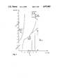
- FIG. 1 is a diagram illustrating the operating range of a prior art circuit/method for protecting a nonvolatile memory device against spurious system-level signals during a power up and power down transition.
- FIG. 2 is a block diagram illustrating the circuit for preventing the erasure and programming of a nonvotatile memory device used in the preferred embodiment of the present invention.
- FIG. 3 is an electric schematic of the power supply generator used in the preferred embodiment of the present invention.
- FIG. 4 is an electric schematic of the reference voltage generator used in the preferred embodiment of the present invention.
- FIG. 5 is an electric schematic of the comparators used in the preferred embodiment of the present invention.
- FIG. 6 is an electric schematic of the Vcc divide-by-two circuit used in the preferred embodiment of the present invention.
- FIG. 7 is an electric schematic of the Vpp divide-by-five circuit used in the preferred embodiment of the present invention.
- FIG. 8 is a diagram illustrating the operating range of the circuit for preventing the erasure and programming of a nonvolatile memory device used in the preferred embodiment of the present invention.
- a circuit for preventing the erasing and programming of a nonvolatile memory device during power up and power down transitions.
- numerous specific details are set forth such as specific conductivity types in order to provide a thorough understanding of the present invention.
- well known elements such as resistors, n-channel devices, p-channel devices, w-channel devices, and other well known fabrication techniques for fabricating the circuits are not described in detail in order not to unnecessarily obscure the present invention.
- a nonvolatile memory device refers to read/write memory in integrated circuit form which retains data whether or not power is applied.
- a nonvolatile memory device includes EPROM, EEPROM and flash memory devices.
- the circuit of the present invention is fabricated along with the entire memory cell on a p-type silicon substrate.
- Ordinary metal-oxide-semiconductor (MOS) processing is employed, and more specifically, complementary metal-oxide-semiconductor (CMOS) technology is used to fabricate the present invention, where n-type devices are formed in the substrate and p-type devices are formed in the n-wells, the n-wells being first formed in the substrate.
- W-channel devices are also used in the present invention.
- a w-channel device is an n-channel device with a gate threshold voltage of approximately 0.0 volts.
- the memory cells employed in the presently preferred embodiment include floating gates which are separated from the channel regions by an oxide thickness of approximately 100°.
- a control gate which is fabricated from a second layer of polysilicon overlies the floating gate. The floating gate is charged by the channel injection of electrons into the floating gate and discharged by the tunneling of charge from the floating gate through the gate oxide.
- the details of the fabrication of the cells are described in a pending patent application, Ser. No. 892,446, filed Aug. 4, 1986, entitled "LOW VOLTAGE EEPROM CELL,” which application is assigned to the assignee of the present invention.
- the flash EPROM memory fabricated with the cells described above receives an externally generated erasing/programming potential Vpp of approximately 12 V and a Vcc voltage of 5 V for normal reading operations.
- the circuits described in FIGS. 2-7 are coupled to the Vpp voltage for putting the nonvolatile memory device into a programming mode and also coupled to the Vcc for putting the nonvolatile memory array in a read mode.
- FIG. 1 is a diagram illustrating the operating range of a prior art circuit for protecting a nonvolatile memory device against spurious system signals during a power up and power down sequence.
- the X-axis of the diagram corresponds to the reading voltage Vcc, and the Y-axis corresponds to the programming voltage Vpp.
- Region low Vcc active 15 and region VppHB active 19 are regions protected by the prior art methods.
- the present invention refers to the steps the manufacturers of memory devices recommend to end users for protecting against accidental erasure or programming of the memory device caused by spurious system-level signals that may exist during the power up and power down transitions. Referring again to FIG.
- region 17 represents the unprotected or unknown regions of the nonvolatile memory device as it proceeds through the power up or power down transition.
- the unknown region 17 is in contrast to the protected or known regions 21 which corresponds to a read only state of the nonvolatile memory device, and region 23 which corresponds to the read/write region of the nonvolatile memory device.
- the state or mode of a nonvolatile memory device is set by a state machine which is also a part of the nonvolatile memory device.
- power up and power down sequence is generally recommended. For instance, during the power up transition, end user is advised to wait until Vcc reaches steady state before applying Vpp.
- the nonvolatile memory device such as the flash EPROM is vulnerable (about 10% of the time) to accidental erasure or programming caused by spurious system level signals that may exist during power up or power down transitions. As a result, the nonvolatile memory device may experience data corruption as a result of over-programming and irreversible damages to the memory array as a result of over-erasure.
- FIG. 2 is a block diagram illustrating the circuit for preventing erasure or programming used in the preferred embodiment of the present invention.
- the circuit 30 comprises a power supply generator 40, a reference voltage 60, a Vcc comparator 80, a Vpp comparator 90, a Vcc divide-by-two circuit 100, and a Vpp divide-by-five circuit 120.
- the power supply generator 40 is coupled to reading voltage Vcc 32 and programming voltage Vpp 34 for generating a node voltage Vpwr 33.
- the node voltage Vpwr 33 is also coupled to the reference voltage generator 60, the Vcc comparator 80, the Vpp comparator 90, the inverter 35, as well as the NOR gate 37.
- the reading voltage Vcc 32 is also coupled to the divide-by-two circuit 100 whose output is also coupled to the Vcc comparator 80.
- programming voltage Vpp 34 is also coupled to the divide-by-five circuit 120, whose output is also coupled to the Vpp comparator 90.
- An optional bypass signal TEST 31 is also coupled to the NOR gate 37.
- the outputs of the circuit 30 are LOWVcc 36 and VppHB 38. It should be understood by one skilled in the art that circuit 30 is one of the many circuits that make up a nonvolatile memory device. It should also be understood by one skilled in the art that the output 36 and 38 of circuit 30 are coupled to a state machine in a nonvolatile memory device which is not shown.
- the state machine of the nonvolatile memory device would either force the nonvolatile memory array into a read or read/write mode (i.e., narrowing the unprotected or unknown region in FIG. 1) in response to receiving the outputs from circuit 30.
- the power supply generator 40 of the circuit 30 provides a node voltage Vpwr 33 for the circuit 30 if either Vcc or Vpp is at a high enough level.
- the power supply generator 40 also allows the detection of both the Vcc and Vpp levels with one circuit.
- the reference voltage generator 60 provides the Vcc comparator 80 and Vpp comparator 90 a reference voltage of nominally 1.75 V to be compared against Vcc divided by two and Vpp divided by 5, thus giving the nominal trip points of 3.5 V and 8.75 V for Vcc and Vpp respectively.
- the outputs of the comparators 80 and 90 are then buffered by the inverter 35 and the NOR gate 37 to drive the output signals for the rest of the nonvolatile memory device, including the state machine and the memory array. Additionally, the VppHB output 38 of the circuit 30 can be optionally overwritten by the TEST signal 31 for other system performance operations such as aging reports.
- FIG. 3 is an electric schematic of the power supply generator used in the preferred embodiment of the present invention.
- the power supply generator 40 comprises n-channel devices 44, 50, 52, 56, p-channel devices 46, 48, 54, w-channel device 42 and a power latch 58.
- the w-channel device 42 and the n-channel device 44 are coupled in a wired-or configuration resulting in a node voltage Vpwr 33.
- N-channel device 44 is diode connected to the programming voltage Vpp 34.
- w-channel device 42 is coupled to the reading voltage Vcc 32.
- the w-channel 42 has a gate threshold voltage of Vtw
- the n-channel device 44 has a gate threshold voltage of Vtn.
- the node voltage Vpwr 33 is the greater of either Vcc-Vtw or Vpp-Vtn.
- the combination of w-channel device 42 and the n-channel device 44 permits the detection of both the Vcc and the Vpp levels with the same circuit. It also follows that with node voltage Vpwr 33, the power supply generator 40 provides a voltage source for the circuit 30 if either Vcc or Vpp is at a high enough level.
- the node voltage Vpwr 33 is also coupled to the p-channel device 54 and the n-channel device 56 for outputting the LOWVcc 36.
- the p-channel device 54 and the n-channel device 56 are also coupled to the Vcc comparator 80 which is not shown in FIG. 3.
- the node voltage Vpwr 33 is also coupled to p-channel devices 46, 48 and n-channel device 50 for outputting VppHB 38.
- the p-channel device 46 and the n-channel device 50 are coupled to the Vpp comparator 90 which is also not shown in FIG. 3.
- Node voltage Vpwr 33 is also coupled to the reference voltage generator 60 for generating a plurality of signals for comparators 80 and 90.
- the reference voltage generator 60 is also not shown in FIG. 3.
- the optional bypass signal TEST 31 is coupled to the p-channel device 46 and the n-channel device 52 over the power latch 58 for optionally overriding the output 38 of the circuit 40.
- the optional bypass signal 31 may be necessary for conducting system performance tests such as aging tests for the nonvolatile memory device.
- FIG. 4 is an electric schematic of the reference voltage generator used in the preferred embodiment of the present invention.
- the reference voltage generator 60 comprises a resistor load 62, w-channel devices 64, 66, and n-channel devices 68, 70, and 72.
- the resistor load 62 is coupled to the node voltage Vpwr 33.
- the resistor load 62 is further coupled to a pair of w-channel devices 64 and 66 and another pair of n-channel devices 68 and 70.
- N-channel devices 70 and 72 also form another pair from which the reference current 74 is outputted.
- the reference voltage 76 is outputted from the w-channel device 64 while the biasing voltage 76 is outputted from the resistor load 62.
- the reference voltage generator 60 is responsible for providing a reference voltage that is stable across process and temperature. As such, a delta-Vt configuration is used.
- the voltage at node voltage Vpwr is (Vtn+Vtn)-(Vtw+Vtw). Because the pair of w-channel devices 64 and 66 and the pair of n-channel devices 68 and 70 have similar variations in process and temperature, this configuration has the desired effect of cancelling their own process and temperature variations.
- the pair of n-channel devices 70 and 72 has a current mirror configuration and as such sets the reference current 74 for the comparators 80, 90.
- FIG. 5 is an electric schematic of the comparators used in the preferred embodiment of the present invention.
- Comparators 80, 90 are identical differential amplifiers and each comprises an n-channel device 82 and a pair of matching n-channel devices 84 and 86, matching pair of w-channel device 92 and 94 and matching p-channel device 96 and 98.
- the matching p-channel device 96 and 98 are coupled to the node voltage Vpwr 33.
- the matching w-channel device 92 and 94 receive the protecting voltage 78 from the reference voltage generator 60.
- N-channel device 84 of the matching pair and device 84 and 86 are coupled to the Vcc divide-by-two circuit 100 and the Vpp divide-by-five circuit 120.
- N-channel device 86 receives the reference voltage 76 from the reference voltage generator 60.
- n-channel device 82 receives the biasing voltage 74 from the reference voltage generator 60.
- the comparators 80, 90 have a single-ended output configuration in output 88. It should be understood by one skilled in the art that comparators 80, 90 are differential amplifier circuits with single-ended outputs.
- N-channel device 82 forms the current source for the amplifier.
- the matched n-channel devices 84, 86 is a differential pair.
- the matched w-channel pair 92, 94 provides protection for the matched n-channel pair 84, 86 against gate-aided breakdown.
- the matched p-channel pair 96, 98 is coupled in a current mirror configuration which is used to convert the various voltages and currents to a single-ended output 88.
- the single-ended output 88 is either coupled to p-channel device 54 and n-channel device 56 or to p-channel device 46 and n-channel device 50, as illustrated in FIG. 3.
- FIG. 6 is an electric schematic of the Vcc divide-by-two circuit used in the preferred embodiment of the present invention.
- the divide-by-two circuit 100 comprises p-channel devices 102, 104, 106, 108, 112, 114, 116, and 118.
- P-channel devices 104 and 114 comprise the nominal divide-by-two circuit, while the rest of the p-channel devices provide a degree of metal mask trimmability.
- the wells of the p-channel devices 102, 104, 106 and 108 are tied to the source so as to eliminate Vt discrepancies due to the body effect.
- the input to the divide-by-two circuit 100 is the reading voltage Vcc, and the output is Vccdiv 99 which is coupled to Vcc comparator 80.
- the p-channel pairs 102, 112, 106, 116 and 108, 118 are not tied to the output line. It should be understood by one skilled in the art that this open arrangement provides a degree of metal mask trimmability for the divide-by-two circuit 100.
- FIG. 7 is an electric schematic of the Vpp divide-by-five circuit used in the preferred embodiment of the present invention.
- the divide-by-five circuit 120 comprises p-channels 122, 124, 126, 128, 130, 132, 134, 136, and 138.
- P-channels 122, 124, 126, 132, and 138 are coupled in a cascading configuration to provide the nominal divide-by-five circuit, while the other p-channel devices provide a degree of metal mask option trimmability.
- the input to the divide-by-five circuit 120 is Vpp, and the output is Vppdiv 140 which is coupled to the Vpp comparator 90.
- FIG. 8 is a diagram illustrating the operating range of the circuit for preventing erasure or programming used in the preferred embodiment of the present invention.
- the X-axis of the diagram in FIG. 8 corresponds to the reading voltage Vcc and the Y-axis corresponds to the programming voltage Vpp.
- the diagram in FIG. 8 should be contrasted with the diagram in FIG. 1.
- Region 156 represents the area where both Vcc and Vpp are sufficiently low such that spurious program and over-erase cannot occur. In this region the voltages are also too low for the circuit to operate.
- Region 150 represents the area where LOW Vcc is active, thus protecting against spurious program and over-erase.
- Region 148 is the area where VppHB is active, thus protecting against spurious program and over-erase.
- Region 151 is the area where end user must assure that no spurious writes occur to the device.
- Region 142 is the valid operating range for updating the flash memory contents. As such, it is not possible to power up or power down the device without passing through the protected region designated by region 148 and region 150.
- the unprotected region 151 as shown in FIG. 8 is substantially smaller than the unprotected region 17 as illustrated in FIG. 1.
- the present invention affords nonvolatile memory devices greater protection against spurious system-level signals during the power up and power down transitions.
Landscapes
- Engineering & Computer Science (AREA)
- Computer Security & Cryptography (AREA)
- Read Only Memory (AREA)
Abstract
Description
Claims (23)
Priority Applications (4)
| Application Number | Priority Date | Filing Date | Title |
|---|---|---|---|
| US07/501,140 US4975883A (en) | 1990-03-29 | 1990-03-29 | Method and apparatus for preventing the erasure and programming of a nonvolatile memory |
| GB9020736A GB2242550B (en) | 1990-03-29 | 1990-09-24 | Apparatus for preventing the erasure and programming of a nonvolatile memory |
| FR909013536A FR2660457B3 (en) | 1990-03-29 | 1990-10-31 | PROTECTIVE CIRCUIT AGAINST ERASING AND PROGRAMMING A REMANENT MEMORY. |
| JP3065366A JPH04221497A (en) | 1990-03-29 | 1991-03-07 | Non-volatile memory-device |
Applications Claiming Priority (1)
| Application Number | Priority Date | Filing Date | Title |
|---|---|---|---|
| US07/501,140 US4975883A (en) | 1990-03-29 | 1990-03-29 | Method and apparatus for preventing the erasure and programming of a nonvolatile memory |
Publications (1)
| Publication Number | Publication Date |
|---|---|
| US4975883A true US4975883A (en) | 1990-12-04 |
Family
ID=23992291
Family Applications (1)
| Application Number | Title | Priority Date | Filing Date |
|---|---|---|---|
| US07/501,140 Expired - Fee Related US4975883A (en) | 1990-03-29 | 1990-03-29 | Method and apparatus for preventing the erasure and programming of a nonvolatile memory |
Country Status (4)
| Country | Link |
|---|---|
| US (1) | US4975883A (en) |
| JP (1) | JPH04221497A (en) |
| FR (1) | FR2660457B3 (en) |
| GB (1) | GB2242550B (en) |
Cited By (60)
| Publication number | Priority date | Publication date | Assignee | Title |
|---|---|---|---|---|
| US5103425A (en) * | 1991-03-11 | 1992-04-07 | Motorola, Inc. | Zener regulated programming circuit for a nonvolatile memory |
| FR2689294A1 (en) * | 1991-11-07 | 1993-10-01 | Samsung Electronics Co Ltd | Voltage pumping circuit for use in semiconductor memory devices. |
| EP0581639A1 (en) * | 1992-07-31 | 1994-02-02 | STMicroelectronics S.A. | Circuit for protecting integrated circuit against cuts in power supply |
| US5295255A (en) * | 1991-02-22 | 1994-03-15 | Electronic Professional Services, Inc. | Method and apparatus for programming a solid state processor with overleaved array memory modules |
| US5301151A (en) * | 1991-05-07 | 1994-04-05 | Intel Corporation | High voltage level converter |
| US5301161A (en) * | 1993-01-12 | 1994-04-05 | Intel Corporation | Circuitry for power supply voltage detection and system lockout for a nonvolatile memory |
| US5345422A (en) * | 1990-07-31 | 1994-09-06 | Texas Instruments Incorporated | Power up detection circuit |
| EP0631285A1 (en) * | 1993-06-25 | 1994-12-28 | Advanced Micro Devices, Inc. | Voltage supply detection and switching system for content addressable memory (CAM) |
| WO1995009483A1 (en) * | 1993-09-30 | 1995-04-06 | Macronix International Co., Ltd. | Improved supply voltage detection circuit |
| US5408435A (en) * | 1990-08-17 | 1995-04-18 | Sgs-Thompson Microelectronics, Inc. | Semiconductor memory with inhibited test mode entry during power-up |
| US5410511A (en) * | 1993-02-24 | 1995-04-25 | Matsushita Electronics Corporation | Methods of controlling the erasing and writing of information in flash memory |
| US5420798A (en) * | 1993-09-30 | 1995-05-30 | Macronix International Co., Ltd. | Supply voltage detection circuit |
| EP0661713A1 (en) * | 1993-12-31 | 1995-07-05 | STMicroelectronics S.r.l. | Threshold voltage detector circuit |
| US5495453A (en) * | 1994-10-19 | 1996-02-27 | Intel Corporation | Low power voltage detector circuit including a flash memory cell |
| EP0700048A1 (en) | 1994-08-31 | 1996-03-06 | STMicroelectronics S.r.l. | Dual sourced voltage supply circuit |
| EP0713166A1 (en) * | 1994-11-15 | 1996-05-22 | STMicroelectronics Limited | A voltage reference circuit |
| EP0713220A1 (en) * | 1994-11-15 | 1996-05-22 | STMicroelectronics Limited | A voltage reference circuit |
| US5537360A (en) * | 1994-09-16 | 1996-07-16 | Dallas Semiconductor Corporation | Programmable power supply systems and methods providing a write protected memory having multiple interface capability |
| US5539337A (en) * | 1994-12-30 | 1996-07-23 | Intel Corporation | Clock noise filter for integrated circuits |
| US5550494A (en) * | 1994-01-25 | 1996-08-27 | Nippon Steel Corporation | Voltage selecting device for receiving a plurality of inputs and selectively outputting one thereof |
| US5566386A (en) * | 1993-03-17 | 1996-10-15 | Fujitsu Limited | Nonvolatile semiconductor memory device having a status register and test method for the same |
| WO1996033496A1 (en) * | 1995-04-21 | 1996-10-24 | Advanced Micro Devices, Inc. | Reference for cmos memory cell having pmos and nmos transistors with a common floating gate |
| US5579196A (en) * | 1993-06-28 | 1996-11-26 | Sgs-Thomson Microelectronics S.R.L. | Protection circuit for devices comprising nonvolatile memories |
| US5586077A (en) * | 1993-12-31 | 1996-12-17 | Sgs-Thomson Microelectronics S.R.L. | Circuit device and corresponding method for resetting non-volatile and electrically programmable memory devices |
| US5594686A (en) * | 1995-12-29 | 1997-01-14 | Intel Corporation | Method and apparatus for protecting data stored in flash memory |
| US5594360A (en) * | 1994-10-19 | 1997-01-14 | Intel Corporation | Low current reduced area programming voltage detector for flash memory |
| US5619450A (en) * | 1991-12-09 | 1997-04-08 | Fujitsu Limited | Drive circuit for flash memory with improved erasability |
| US5663918A (en) * | 1994-10-19 | 1997-09-02 | Intel Corporation | Method and apparatus for detecting and selecting voltage supplies for flash memory |
| US5959926A (en) * | 1996-06-07 | 1999-09-28 | Dallas Semiconductor Corp. | Programmable power supply systems and methods providing a write protected memory having multiple interface capability |
| US6011679A (en) * | 1998-09-30 | 2000-01-04 | Digital Equipment Corp. | Methods and apparatus for controlling a power supply with improved techniques for providing protection limits |
| EP0974145A1 (en) * | 1997-04-11 | 2000-01-26 | Intel Corporation | Power supply detection scheme for flash memory |
| US6243282B1 (en) | 1996-05-15 | 2001-06-05 | Micron Technology Inc. | Apparatus for on-board programming of serial EEPROMs |
| US20030112681A1 (en) * | 1995-02-10 | 2003-06-19 | Micron Technology, Inc. | Fast-sensing amplifier for flash memory |
| US6628552B1 (en) | 1997-04-11 | 2003-09-30 | Intel Corporation | Self-configuring input buffer on flash memories |
| US6629047B1 (en) * | 2000-03-30 | 2003-09-30 | Intel Corporation | Method and apparatus for flash voltage detection and lockout |
| EP1367595A1 (en) * | 2002-05-27 | 2003-12-03 | Valeo Schalter und Sensoren GmbH | EEPROM and method for programming and erasing of an EEPROM |
| US20040228178A1 (en) * | 2003-05-12 | 2004-11-18 | Sharp Kabushiki Kaisha | Semiconductor memory device with malfunction prevention device, and portable eletronic apparatus using the same |
| US20040237010A1 (en) * | 1992-05-20 | 2004-11-25 | Auclair Daniel L. | Soft errors handling in EEPROM devices |
| EP1469479A3 (en) * | 1997-01-08 | 2005-11-02 | Micron Technology, Inc. | Programming voltage protection in non-volatine memory system |
| US20060190646A1 (en) * | 2004-03-10 | 2006-08-24 | Silicon Storage Technology, Inc. | Motherboard having a non-volatile memory which is reprogrammable through a video display port |
| US20070010967A1 (en) * | 2005-06-30 | 2007-01-11 | Wolfgang Scherr | Holding Device for a Sensor Signal, Method for Forwarding a Sensor Signal and Computer Program |
| US20070104004A1 (en) * | 1997-09-08 | 2007-05-10 | So Hock C | Multi-Bit-Per-Cell Flash EEprom Memory with Refresh |
| US7219263B1 (en) * | 2003-10-29 | 2007-05-15 | Qlogic, Corporation | Method and system for minimizing memory corruption |
| US20080239808A1 (en) * | 2007-03-28 | 2008-10-02 | Lin Jason T | Flash Memory Refresh Techniques Triggered by Controlled Scrub Data Reads |
| US20080239851A1 (en) * | 2007-03-28 | 2008-10-02 | Lin Jason T | Flash Memory with Data Refresh Triggered by Controlled Scrub Data Reads |
| US7518919B2 (en) | 2003-10-03 | 2009-04-14 | Sandisk Corporation | Flash memory data correction and scrub techniques |
| US7669190B2 (en) | 2004-05-18 | 2010-02-23 | Qlogic, Corporation | Method and system for efficiently recording processor events in host bus adapters |
| US20100106891A1 (en) * | 2008-10-29 | 2010-04-29 | Microchip Technology Incorporated | Preventing Unintended Permanent Write-Protection |
| US7716538B2 (en) | 2006-09-27 | 2010-05-11 | Sandisk Corporation | Memory with cell population distribution assisted read margining |
| US7886204B2 (en) | 2006-09-27 | 2011-02-08 | Sandisk Corporation | Methods of cell population distribution assisted read margining |
| AU2008242339B2 (en) * | 2007-04-16 | 2012-04-19 | Itt Manufacturing Enterprises, Inc. | Appliance controller system featuring automatic beverage dispenser shutoff system |
| US8687421B2 (en) | 2011-11-21 | 2014-04-01 | Sandisk Technologies Inc. | Scrub techniques for use with dynamic read |
| US9230689B2 (en) | 2014-03-17 | 2016-01-05 | Sandisk Technologies Inc. | Finding read disturbs on non-volatile memories |
| US9349479B1 (en) | 2014-11-18 | 2016-05-24 | Sandisk Technologies Inc. | Boundary word line operation in nonvolatile memory |
| US9449700B2 (en) | 2015-02-13 | 2016-09-20 | Sandisk Technologies Llc | Boundary word line search and open block read methods with reduced read disturb |
| US9552171B2 (en) | 2014-10-29 | 2017-01-24 | Sandisk Technologies Llc | Read scrub with adaptive counter management |
| US9653154B2 (en) | 2015-09-21 | 2017-05-16 | Sandisk Technologies Llc | Write abort detection for multi-state memories |
| EP3055865A4 (en) * | 2013-11-11 | 2017-06-21 | Samsung Electronics Co., Ltd. | Method and device for protecting data of flash memory |
| US9978456B2 (en) | 2014-11-17 | 2018-05-22 | Sandisk Technologies Llc | Techniques for reducing read disturb in partially written blocks of non-volatile memory |
| US11081156B2 (en) * | 2019-07-05 | 2021-08-03 | Arm Limited | Voltage regulation circuitry |
Families Citing this family (1)
| Publication number | Priority date | Publication date | Assignee | Title |
|---|---|---|---|---|
| JP5348541B2 (en) * | 2009-05-20 | 2013-11-20 | ルネサスエレクトロニクス株式会社 | Semiconductor device |
Citations (3)
| Publication number | Priority date | Publication date | Assignee | Title |
|---|---|---|---|---|
| US4433390A (en) * | 1981-07-30 | 1984-02-21 | The Bendix Corporation | Power processing reset system for a microprocessor responding to sudden deregulation of a voltage |
| US4712195A (en) * | 1986-05-09 | 1987-12-08 | Curtis Instruments, Inc. | Solid-state cumulative operations measurement system |
| US4777626A (en) * | 1984-12-22 | 1988-10-11 | Tokyo Electric Co., Ltd. | Memory device having backup power supply |
Family Cites Families (3)
| Publication number | Priority date | Publication date | Assignee | Title |
|---|---|---|---|---|
| US4439804A (en) * | 1982-03-22 | 1984-03-27 | Rca Corporation | Protection circuit for memory programming system |
| US4612632A (en) * | 1984-12-10 | 1986-09-16 | Zenith Electronics Corporation | Power transition write protection for PROM |
| FR2604555B1 (en) * | 1986-09-30 | 1988-11-10 | Eurotechnique Sa | INTEGRATED CIRCUIT OF THE LOGIC CIRCUIT TYPE COMPRISING AN ELECTRICALLY PROGRAMMABLE NON-VOLATILE MEMORY |
-
1990
- 1990-03-29 US US07/501,140 patent/US4975883A/en not_active Expired - Fee Related
- 1990-09-24 GB GB9020736A patent/GB2242550B/en not_active Expired - Lifetime
- 1990-10-31 FR FR909013536A patent/FR2660457B3/en not_active Expired - Lifetime
-
1991
- 1991-03-07 JP JP3065366A patent/JPH04221497A/en active Pending
Patent Citations (3)
| Publication number | Priority date | Publication date | Assignee | Title |
|---|---|---|---|---|
| US4433390A (en) * | 1981-07-30 | 1984-02-21 | The Bendix Corporation | Power processing reset system for a microprocessor responding to sudden deregulation of a voltage |
| US4777626A (en) * | 1984-12-22 | 1988-10-11 | Tokyo Electric Co., Ltd. | Memory device having backup power supply |
| US4712195A (en) * | 1986-05-09 | 1987-12-08 | Curtis Instruments, Inc. | Solid-state cumulative operations measurement system |
Cited By (97)
| Publication number | Priority date | Publication date | Assignee | Title |
|---|---|---|---|---|
| US5345422A (en) * | 1990-07-31 | 1994-09-06 | Texas Instruments Incorporated | Power up detection circuit |
| US5408435A (en) * | 1990-08-17 | 1995-04-18 | Sgs-Thompson Microelectronics, Inc. | Semiconductor memory with inhibited test mode entry during power-up |
| US5706232A (en) * | 1990-08-17 | 1998-01-06 | Sgs-Thomson Microelectronics, Inc. | Semiconductor memory with multiple clocking for test mode entry |
| US5295255A (en) * | 1991-02-22 | 1994-03-15 | Electronic Professional Services, Inc. | Method and apparatus for programming a solid state processor with overleaved array memory modules |
| US5103425A (en) * | 1991-03-11 | 1992-04-07 | Motorola, Inc. | Zener regulated programming circuit for a nonvolatile memory |
| US5301151A (en) * | 1991-05-07 | 1994-04-05 | Intel Corporation | High voltage level converter |
| FR2689294A1 (en) * | 1991-11-07 | 1993-10-01 | Samsung Electronics Co Ltd | Voltage pumping circuit for use in semiconductor memory devices. |
| US5619450A (en) * | 1991-12-09 | 1997-04-08 | Fujitsu Limited | Drive circuit for flash memory with improved erasability |
| US20050083726A1 (en) * | 1992-05-20 | 2005-04-21 | Auclair Daniel L. | Soft errors handling EEPROM devices |
| US20040237010A1 (en) * | 1992-05-20 | 2004-11-25 | Auclair Daniel L. | Soft errors handling in EEPROM devices |
| US20050058008A1 (en) * | 1992-05-20 | 2005-03-17 | Auclair Daniel L. | Soft errors handling in eeprom devices |
| US7839685B2 (en) | 1992-05-20 | 2010-11-23 | Sandisk Corporation | Soft errors handling in EEPROM devices |
| US7616484B2 (en) | 1992-05-20 | 2009-11-10 | Sandisk Corporation | Soft errors handling in EEPROM devices |
| US7548461B2 (en) * | 1992-05-20 | 2009-06-16 | Sandisk Corporation | Soft errors handling in EEPROM devices |
| US7437631B2 (en) | 1992-05-20 | 2008-10-14 | Sandisk Corporation | Soft errors handling in EEPROM devices |
| FR2694448A1 (en) * | 1992-07-31 | 1994-02-04 | Sgs Thomson Microelectronics | Device for protecting an integrated circuit against power cuts. |
| EP0581639A1 (en) * | 1992-07-31 | 1994-02-02 | STMicroelectronics S.A. | Circuit for protecting integrated circuit against cuts in power supply |
| US5473496A (en) * | 1992-07-31 | 1995-12-05 | Sgs-Thomson Microelectronics, S.A. | Device for the protection of an integrated circuit against power supply cuts |
| US5301161A (en) * | 1993-01-12 | 1994-04-05 | Intel Corporation | Circuitry for power supply voltage detection and system lockout for a nonvolatile memory |
| US5410511A (en) * | 1993-02-24 | 1995-04-25 | Matsushita Electronics Corporation | Methods of controlling the erasing and writing of information in flash memory |
| US5566386A (en) * | 1993-03-17 | 1996-10-15 | Fujitsu Limited | Nonvolatile semiconductor memory device having a status register and test method for the same |
| EP0631285A1 (en) * | 1993-06-25 | 1994-12-28 | Advanced Micro Devices, Inc. | Voltage supply detection and switching system for content addressable memory (CAM) |
| US5579196A (en) * | 1993-06-28 | 1996-11-26 | Sgs-Thomson Microelectronics S.R.L. | Protection circuit for devices comprising nonvolatile memories |
| US5420798A (en) * | 1993-09-30 | 1995-05-30 | Macronix International Co., Ltd. | Supply voltage detection circuit |
| WO1995009483A1 (en) * | 1993-09-30 | 1995-04-06 | Macronix International Co., Ltd. | Improved supply voltage detection circuit |
| US5583820A (en) * | 1993-12-31 | 1996-12-10 | Sgs-Thomson Microelectronics S.R.L. | Device for detecting a reduction in a supply voltage |
| US5586077A (en) * | 1993-12-31 | 1996-12-17 | Sgs-Thomson Microelectronics S.R.L. | Circuit device and corresponding method for resetting non-volatile and electrically programmable memory devices |
| EP0661713A1 (en) * | 1993-12-31 | 1995-07-05 | STMicroelectronics S.r.l. | Threshold voltage detector circuit |
| US5748548A (en) * | 1993-12-31 | 1998-05-05 | Sgs-Thomson Microelectronics S.R.L. | Device for detecting a reduction in a supply voltage |
| US5550494A (en) * | 1994-01-25 | 1996-08-27 | Nippon Steel Corporation | Voltage selecting device for receiving a plurality of inputs and selectively outputting one thereof |
| US5719490A (en) * | 1994-08-31 | 1998-02-17 | Sgs-Thomson Microelectronics S.R.L. | Dual sourced voltage supply circuit |
| EP0700048A1 (en) | 1994-08-31 | 1996-03-06 | STMicroelectronics S.r.l. | Dual sourced voltage supply circuit |
| US5537360A (en) * | 1994-09-16 | 1996-07-16 | Dallas Semiconductor Corporation | Programmable power supply systems and methods providing a write protected memory having multiple interface capability |
| US5594360A (en) * | 1994-10-19 | 1997-01-14 | Intel Corporation | Low current reduced area programming voltage detector for flash memory |
| US5495453A (en) * | 1994-10-19 | 1996-02-27 | Intel Corporation | Low power voltage detector circuit including a flash memory cell |
| US5663918A (en) * | 1994-10-19 | 1997-09-02 | Intel Corporation | Method and apparatus for detecting and selecting voltage supplies for flash memory |
| EP0713166A1 (en) * | 1994-11-15 | 1996-05-22 | STMicroelectronics Limited | A voltage reference circuit |
| US5610506A (en) * | 1994-11-15 | 1997-03-11 | Sgs-Thomson Microelectronics Limited | Voltage reference circuit |
| US5831302A (en) * | 1994-11-15 | 1998-11-03 | Sgs-Thomson Microelectronics Limited | Voltage reference circuit |
| EP0713220A1 (en) * | 1994-11-15 | 1996-05-22 | STMicroelectronics Limited | A voltage reference circuit |
| US5539337A (en) * | 1994-12-30 | 1996-07-23 | Intel Corporation | Clock noise filter for integrated circuits |
| US20040170078A1 (en) * | 1995-02-10 | 2004-09-02 | Micron Technology, Inc. | Read-biasing and amplifying system |
| US20030112681A1 (en) * | 1995-02-10 | 2003-06-19 | Micron Technology, Inc. | Fast-sensing amplifier for flash memory |
| US6996010B2 (en) | 1995-02-10 | 2006-02-07 | Micron Technology, Inc. | Fast-sensing amplifier for flash memory |
| US6744673B2 (en) * | 1995-02-10 | 2004-06-01 | Micron Technology, Inc. | Feedback biasing integrated circuit |
| US6914822B2 (en) | 1995-02-10 | 2005-07-05 | Micron Technology Inc. | Read-biasing and amplifying system |
| WO1996033496A1 (en) * | 1995-04-21 | 1996-10-24 | Advanced Micro Devices, Inc. | Reference for cmos memory cell having pmos and nmos transistors with a common floating gate |
| US5796295A (en) * | 1995-04-21 | 1998-08-18 | Advanced Micro Devices, Inc. | Reference for CMOS memory cell having PMOS and NMOS transistors with a common floating gate |
| US5594686A (en) * | 1995-12-29 | 1997-01-14 | Intel Corporation | Method and apparatus for protecting data stored in flash memory |
| US6256217B1 (en) | 1996-05-15 | 2001-07-03 | Micron Technology, Inc. | Apparatus for on-board programming of serial EEPROMS |
| US6519172B2 (en) | 1996-05-15 | 2003-02-11 | Micron Technology, Inc. | Apparatus for on-board programming of serial EEPROMS |
| US6243282B1 (en) | 1996-05-15 | 2001-06-05 | Micron Technology Inc. | Apparatus for on-board programming of serial EEPROMs |
| US5959926A (en) * | 1996-06-07 | 1999-09-28 | Dallas Semiconductor Corp. | Programmable power supply systems and methods providing a write protected memory having multiple interface capability |
| EP1469479A3 (en) * | 1997-01-08 | 2005-11-02 | Micron Technology, Inc. | Programming voltage protection in non-volatine memory system |
| US6628552B1 (en) | 1997-04-11 | 2003-09-30 | Intel Corporation | Self-configuring input buffer on flash memories |
| EP0974145A1 (en) * | 1997-04-11 | 2000-01-26 | Intel Corporation | Power supply detection scheme for flash memory |
| EP0974145A4 (en) * | 1997-04-11 | 2001-04-18 | Intel Corp | Power supply detection scheme for flash memory |
| US7397697B2 (en) | 1997-09-08 | 2008-07-08 | Sandisk Corporation | Multi-bit-per-cell flash EEPROM memory with refresh |
| US20070104004A1 (en) * | 1997-09-08 | 2007-05-10 | So Hock C | Multi-Bit-Per-Cell Flash EEprom Memory with Refresh |
| US6011679A (en) * | 1998-09-30 | 2000-01-04 | Digital Equipment Corp. | Methods and apparatus for controlling a power supply with improved techniques for providing protection limits |
| US6789027B2 (en) | 2000-03-30 | 2004-09-07 | Intel Corporation | Method and apparatus for flash voltage detection and lockout |
| US6629047B1 (en) * | 2000-03-30 | 2003-09-30 | Intel Corporation | Method and apparatus for flash voltage detection and lockout |
| EP1367595A1 (en) * | 2002-05-27 | 2003-12-03 | Valeo Schalter und Sensoren GmbH | EEPROM and method for programming and erasing of an EEPROM |
| US6977843B2 (en) | 2003-05-12 | 2005-12-20 | Sharp Kabushiki Kaisha | Semiconductor memory device with malfunction prevention device, and portable electronic apparatus using the same |
| US20040228178A1 (en) * | 2003-05-12 | 2004-11-18 | Sharp Kabushiki Kaisha | Semiconductor memory device with malfunction prevention device, and portable eletronic apparatus using the same |
| US8004895B2 (en) | 2003-10-03 | 2011-08-23 | Sandisk Technologies Inc. | Flash memory data correction and scrub techniques |
| US8050095B2 (en) | 2003-10-03 | 2011-11-01 | Sandisk Technologies Inc. | Flash memory data correction and scrub techniques |
| US7518919B2 (en) | 2003-10-03 | 2009-04-14 | Sandisk Corporation | Flash memory data correction and scrub techniques |
| US7219263B1 (en) * | 2003-10-29 | 2007-05-15 | Qlogic, Corporation | Method and system for minimizing memory corruption |
| US7146442B2 (en) * | 2004-03-10 | 2006-12-05 | Silicon Storage Technology, Inc. | Motherboard having a non-volatile memory which is reprogrammable through a video display port |
| US20060190646A1 (en) * | 2004-03-10 | 2006-08-24 | Silicon Storage Technology, Inc. | Motherboard having a non-volatile memory which is reprogrammable through a video display port |
| US7669190B2 (en) | 2004-05-18 | 2010-02-23 | Qlogic, Corporation | Method and system for efficiently recording processor events in host bus adapters |
| US20070010967A1 (en) * | 2005-06-30 | 2007-01-11 | Wolfgang Scherr | Holding Device for a Sensor Signal, Method for Forwarding a Sensor Signal and Computer Program |
| US7369969B2 (en) * | 2005-06-30 | 2008-05-06 | Infineon Technologies Ag | Holding device for a sensor signal, method for forwarding a sensor signal and computer program |
| US7716538B2 (en) | 2006-09-27 | 2010-05-11 | Sandisk Corporation | Memory with cell population distribution assisted read margining |
| US7886204B2 (en) | 2006-09-27 | 2011-02-08 | Sandisk Corporation | Methods of cell population distribution assisted read margining |
| US8473813B2 (en) | 2006-09-27 | 2013-06-25 | Sandisk Technologies Inc. | Methods of cell population distribution assisted read margining |
| US7573773B2 (en) | 2007-03-28 | 2009-08-11 | Sandisk Corporation | Flash memory with data refresh triggered by controlled scrub data reads |
| US20080239851A1 (en) * | 2007-03-28 | 2008-10-02 | Lin Jason T | Flash Memory with Data Refresh Triggered by Controlled Scrub Data Reads |
| US7477547B2 (en) | 2007-03-28 | 2009-01-13 | Sandisk Corporation | Flash memory refresh techniques triggered by controlled scrub data reads |
| US20080239808A1 (en) * | 2007-03-28 | 2008-10-02 | Lin Jason T | Flash Memory Refresh Techniques Triggered by Controlled Scrub Data Reads |
| AU2008242339B2 (en) * | 2007-04-16 | 2012-04-19 | Itt Manufacturing Enterprises, Inc. | Appliance controller system featuring automatic beverage dispenser shutoff system |
| CN102187401B (en) * | 2008-10-29 | 2014-06-18 | 密克罗奇普技术公司 | Preventing unintended permanent write-protection in nonvolatile memory |
| WO2010053749A1 (en) * | 2008-10-29 | 2010-05-14 | Microchip Technology Incorporated | Preventing unintended permanent write-protection in nonvolatile memory |
| US20100106891A1 (en) * | 2008-10-29 | 2010-04-29 | Microchip Technology Incorporated | Preventing Unintended Permanent Write-Protection |
| CN102187401A (en) * | 2008-10-29 | 2011-09-14 | 密克罗奇普技术公司 | Preventing unintended permanent write-protection in nonvolatile memory |
| US8117378B2 (en) | 2008-10-29 | 2012-02-14 | Microchip Technology Incorporated | Preventing unintended permanent write-protection |
| US8687421B2 (en) | 2011-11-21 | 2014-04-01 | Sandisk Technologies Inc. | Scrub techniques for use with dynamic read |
| EP3055865A4 (en) * | 2013-11-11 | 2017-06-21 | Samsung Electronics Co., Ltd. | Method and device for protecting data of flash memory |
| US9230689B2 (en) | 2014-03-17 | 2016-01-05 | Sandisk Technologies Inc. | Finding read disturbs on non-volatile memories |
| US9552171B2 (en) | 2014-10-29 | 2017-01-24 | Sandisk Technologies Llc | Read scrub with adaptive counter management |
| US9978456B2 (en) | 2014-11-17 | 2018-05-22 | Sandisk Technologies Llc | Techniques for reducing read disturb in partially written blocks of non-volatile memory |
| US9349479B1 (en) | 2014-11-18 | 2016-05-24 | Sandisk Technologies Inc. | Boundary word line operation in nonvolatile memory |
| US9449700B2 (en) | 2015-02-13 | 2016-09-20 | Sandisk Technologies Llc | Boundary word line search and open block read methods with reduced read disturb |
| US9653154B2 (en) | 2015-09-21 | 2017-05-16 | Sandisk Technologies Llc | Write abort detection for multi-state memories |
| US9899077B2 (en) | 2015-09-21 | 2018-02-20 | Sandisk Technologies Llc | Write abort detection for multi-state memories |
| US11081156B2 (en) * | 2019-07-05 | 2021-08-03 | Arm Limited | Voltage regulation circuitry |
Also Published As
| Publication number | Publication date |
|---|---|
| GB9020736D0 (en) | 1990-11-07 |
| GB2242550A (en) | 1991-10-02 |
| FR2660457A1 (en) | 1991-10-04 |
| JPH04221497A (en) | 1992-08-11 |
| GB2242550B (en) | 1994-09-28 |
| FR2660457B3 (en) | 1992-07-10 |
Similar Documents
| Publication | Publication Date | Title |
|---|---|---|
| US4975883A (en) | Method and apparatus for preventing the erasure and programming of a nonvolatile memory | |
| KR950000273B1 (en) | Non-volatile semiconductor memory device and optimal write method | |
| US6807098B2 (en) | Nonvolatile semiconductor memory with a programming operation and the method thereof | |
| US6262926B1 (en) | Nonvolatile semiconductor memory device | |
| US4841482A (en) | Leakage verification for flash EPROM | |
| US6288944B1 (en) | NAND type nonvolatile memory with improved erase-verify operations | |
| US6181605B1 (en) | Global erase/program verification apparatus and method | |
| KR100221939B1 (en) | Semiconductor memory device and high-voltage switching circuit | |
| US20040004861A1 (en) | Differential EEPROM using pFET floating gate transistors | |
| US5576992A (en) | Extended-life method for soft-programming floating-gate memory cells | |
| US5136541A (en) | Programmable read only memory using stacked-gate cell erasable by hole injection | |
| US20020080653A1 (en) | Method for preventing over-erasing of memory cells and flash memory device using the same | |
| US7460411B2 (en) | Array source line (AVSS) controlled high voltage regulation for programming flash or EE array | |
| EP0548866B1 (en) | Non-volatile semiconductor memory device | |
| US6137729A (en) | Method for erasing memory cells in a flash memory device | |
| US5450417A (en) | Circuit for testing power-on-reset circuitry | |
| US6031774A (en) | Internal power supply voltage generating ciruit and the method for controlling thereof | |
| US5220528A (en) | Compensation circuit for leakage in flash EPROM | |
| KR19990036007A (en) | Flash memory system and method with reduced interference | |
| US5397946A (en) | High-voltage sensor for integrated circuits | |
| US6954379B2 (en) | Power-on reset circuit for erasing of split gate flash memory reference cells | |
| US5903497A (en) | Integrated program verify page buffer | |
| US5253200A (en) | Electrically erasable and programmable read only memory using stacked-gate cell | |
| US6262622B1 (en) | Breakdown-free high voltage input circuitry | |
| JP3544222B2 (en) | Nonvolatile semiconductor memory device |
Legal Events
| Date | Code | Title | Description |
|---|---|---|---|
| AS | Assignment |
Owner name: INTEL CORPORATION, CALIFORNIA Free format text: ASSIGNMENT OF ASSIGNORS INTEREST.;ASSIGNORS:BAKER, ALAN E.;DURANTE, RICHARD J.;JUNGROTH, OWEN W.;REEL/FRAME:005343/0205 Effective date: 19900525 |
|
| FEPP | Fee payment procedure |
Free format text: PAYOR NUMBER ASSIGNED (ORIGINAL EVENT CODE: ASPN); ENTITY STATUS OF PATENT OWNER: LARGE ENTITY |
|
| FPAY | Fee payment |
Year of fee payment: 4 |
|
| REMI | Maintenance fee reminder mailed | ||
| FPAY | Fee payment |
Year of fee payment: 8 |
|
| REMI | Maintenance fee reminder mailed | ||
| LAPS | Lapse for failure to pay maintenance fees | ||
| STCH | Information on status: patent discontinuation |
Free format text: PATENT EXPIRED DUE TO NONPAYMENT OF MAINTENANCE FEES UNDER 37 CFR 1.362 |
|
| FP | Lapsed due to failure to pay maintenance fee |
Effective date: 20021204 |