US4978224A - Method of and apparatus for inspecting mounting of chip components - Google Patents

Method of and apparatus for inspecting mounting of chip components Download PDF

Info

Publication number
US4978224A
US4978224A US07/218,311 US21831188A US4978224A US 4978224 A US4978224 A US 4978224A US 21831188 A US21831188 A US 21831188A US 4978224 A US4978224 A US 4978224A
Authority
US
United States
Prior art keywords
circuit board
slit
light
image
components
Prior art date
Legal status (The legal status is an assumption and is not a legal conclusion. Google has not performed a legal analysis and makes no representation as to the accuracy of the status listed.)
Expired - Fee Related
Application number
US07/218,311
Inventor
Shin Kishimoto
Toshihide Morimoto
Nobuaki Kakimori
Yuho Takahashi
Morihide Ohsaki
Current Assignee (The listed assignees may be inaccurate. Google has not performed a legal analysis and makes no representation or warranty as to the accuracy of the list.)
Sharp Corp
Original Assignee
Sharp Corp
Priority date (The priority date is an assumption and is not a legal conclusion. Google has not performed a legal analysis and makes no representation as to the accuracy of the date listed.)
Filing date
Publication date
Priority claimed from JP62175224A external-priority patent/JPS6418004A/en
Priority claimed from JP62175225A external-priority patent/JPS6418049A/en
Priority claimed from JP24665787A external-priority patent/JPS6488204A/en
Priority claimed from JP32208687A external-priority patent/JPH01161310A/en
Priority claimed from JP32606187A external-priority patent/JPH01165903A/en
Application filed by Sharp Corp filed Critical Sharp Corp
Assigned to SHARP KABUSHIKI KAISHA, reassignment SHARP KABUSHIKI KAISHA, ASSIGNMENT OF ASSIGNORS INTEREST. Assignors: KAKIMORI, NOBUAKI, KISHIMOTO, SHIN, MORIMOTO, TOSHIHIDE, OHSAKI, MORIHIDE, TAKAHASHI, YUHO
Application granted granted Critical
Publication of US4978224A publication Critical patent/US4978224A/en
Anticipated expiration legal-status Critical
Expired - Fee Related legal-status Critical Current

Links

Images

Classifications

    • HELECTRICITY
    • H05ELECTRIC TECHNIQUES NOT OTHERWISE PROVIDED FOR
    • H05KPRINTED CIRCUITS; CASINGS OR CONSTRUCTIONAL DETAILS OF ELECTRIC APPARATUS; MANUFACTURE OF ASSEMBLAGES OF ELECTRICAL COMPONENTS
    • H05K13/00Apparatus or processes specially adapted for manufacturing or adjusting assemblages of electric components
    • H05K13/08Monitoring manufacture of assemblages
    • H05K13/081Integration of optical monitoring devices in assembly lines; Processes using optical monitoring devices specially adapted for controlling devices or machines in assembly lines
    • H05K13/0815Controlling of component placement on the substrate during or after manufacturing

Definitions

  • This invention relates to a method of and apparatus for automatically inspecting whether chip components mounted on a printed circuit board have been set correctly or not.
  • the above and other objects of the present invention can be achieved by exposing the mounted printed circuit board to be tested to a plurality of slit light beams made incident thereon diagonally from above and extracting image data from the slit line image pattern created by the chip components which protrude three-dimensionally from the otherwise flat surface of the circuit board. Positions, sizes and orientations of individual chip components mounted on the circuit board can be calculated from such image data and compared with initially inputted data based on the information how these components are expected to be mounted.
  • each source of slit light beams is provided with a mirror of which the orientation can be adjusted. Thus, if no component is identified at a position where it is anticipated to be, the mirror angle is changed to increase or decrease the projection angle.
  • the present invention also teaches a method whereby a center point in the slit line image is selected as a starting point and brightness at points at a specified distance away is compared with a threshold brightness value.
  • a shutter system of a simple structure with a disk rotatably supported where the two light paths for projecting the line images in two directions cross each other.
  • the disk has a window such that these two light paths are alternately blocked as the disk is rotated.
  • the edge positions of chip components mounted on a printed circuit board can be determined accurately and quickly. Since data on anticipated positions, sizes, orientations, etc. of chip components mounted on a circuit board are readily available, measured data can be easily evaluated. Since the inspection procedure can be fully automated, errors become infrequent and reliability of inspection improves significantly.
  • prior art inspection apparatus were designed to inspect only one chip at a time, the present invention teaches receiving image data of many chips within a field of vision at once and hence improves efficiency of inspection. Moreover, the image receiving device can be moved from one viewing position to another while the data obtained from the first position are being analyzed. This capability adds to the improvement in efficiency. Additional advantages of the present invention include that accuracy is not adversely affected by changes in image density and that light beams can be switched on and off by a relatively inexpensive mechanism relying only on a simply rotary motion of a disk.
  • FIG. 1 is a block diagram of an apparatus embodying the present invention
  • FIGS. 2A and 2B are examples of slit line patterns formed by slit line beams on a mounted circuit board
  • FIG. 3 is a plan view of a mounted circuit board partitioned into areas for inspection according to a method embodying the present invention
  • FIG. 4 is a plan view of one of the partitioned areas shown in FIG. 3,
  • FIGS. 5A-5C are plan views of slit line patterns by a component mounted on a circuit board
  • FIGS. 6A-6C are plan views of windows used in an inspection method of the present invention.
  • FIG. 7 is a flow chart showing an inspection method embodying the present invention.
  • FIGS. 8A and 8B are drawings for showing a method of determining an end point of a slit line image
  • FIGS. 9, 10A and 10B are examples of slit line image
  • FIG. 11A is a side view of a component soldered onto a circuit board and FIG. 11B is a slit line pattern obtained from the soldered component shown in FIG. 11A,
  • FIGS. 12A and 12B are examples of stored image data corresponding to a portion of the pattern shown in FIG. 11B,
  • FIG. 13 is a block diagram of another apparatus embodying the present invention of the type shown in FIG. 1 with portions thereof shown more in detail,
  • FIG. 14 is a flow chart showing portions of FIG. 7 more in detail
  • FIGS. 15, 16 and 17 are drawings for showing the concept of and a method of using frames in an inspection method embodying the present invention
  • FIG. 18 is a schematic drawing of a light source unit embodying the present invention.
  • FIGS. 19A and 19B are drawings for showing slit line patterns before and after the projection angle is changed by the system shown in FIG. 18,
  • FIG. 20 is a block diagram of another apparatus embodying the present invention of the type shown in FIGS. 1 and 13 with some portions thereof shown more in detail,
  • FIG. 21 is a schematic drawing of a shutter system embodying the present invention.
  • FIG. 22 is a front view of the disk shown in FIG. 21,
  • FIG. 23 is a schematic plan view of the position sensor shown in FIG. 21,
  • FIG. 24 is a schematic side view of the position sensor of FIGS. 21 and 23,
  • FIG. 25 is a schematic drawing showing positional relationships of the disk and the position sensor of FIG. 21 with respect to the light paths from the light sources,
  • FIG. 26 is a flow chart showing the operation of the shutter system of FIG. 21,
  • FIG. 27 is a signal waveform chart for the operation by a method according to the present invention.
  • FIGS. 28A-28E are schematic plan views for showing positional relationships between the angular orientation of the disk and the light paths
  • FIG. 29 is a plan view of a prior art iris-type mechanical lens shutter.
  • FIG. 30 is a signal wave form chart associated with a prior art shutter system.
  • a printed circuit board 3 with chip components 5 mounted thereon is placed on top of a table 4 which is freely movable two-dimensionally in X- and Y-directions as shown.
  • a table 4 which is freely movable two-dimensionally in X- and Y-directions as shown.
  • two sources of slit light beams 1X and 2Y respectively for the direction of the X-axis and the Y-axis are placed diagonally above the table 4.
  • Each of these light sources 1X and 1Y is provided with a shutter 2X or 2Y such that line beams in the X- and Y-directions can be selectably and separately made incident on the mounted chip components 5 by controlling these shutters 2X and 2Y.
  • An image receiving device 6 such as a camera is disposed above the printed circuit board 3 for receiving an image of the target objects as well as of their surroundings.
  • An analog-to-digital (A/D) converter 7, an image processing device 8 to be described below more in detail and a control circuit 9 are serially connected to this image receiving device 6.
  • the control circuit 9 is also connected to a table driving circuit 10 for moving the table 4 so as to control its motion through an X-direction driver 11X and a Y-direction driver 11Y.
  • the X- and Y-direction drivers 11X and 11Y are operated by a signal transmitted from the control circuit 9 to the table driving circuit 10 such that those of the mounted chip components 5 on the printed circuit board 3 to be inspected come within the viewing range of the image receiving device 6.
  • the shutter 2X on the X-direction light line source 1X is operated to project lines of light in the X-direction on these target components 5 and the slit pattern image obtained thereby is viewed from above by the image receiving device 6.
  • the shutter 2Y on the Y-direction light line source 1Y is operated to project lines of light in the Y-direction and the slit pattern image thus obtained is similarly viewed by the image receiving device 6.
  • Image data corresponding to these pattern images are converted into a digital signal by the analog-to-digital converter 7.
  • the image of the light lines change according to their three-dimensional shapes. Near the outer peripheries of a viewing range, in particular, the image of the light lines become discontinuous, making it possible to detect the shape of these chip components 5.
  • the digitally converted data are transmitted to the image processing device 8 where detection, calculation and judging circuits cooperate to detect the edges of the slit lines, calculate characteristic values of various kinds and eventually evaluate on the basis of such values whether the chip components 5 under investigation are properly mounted. The same procedure is repeated after the table 4 is moved and the conditions of all chip components 5 on the printed circuit board 3 can be inspected in this manner.
  • FIGS. 2A and 2B show examples of slit patterns projected on a chip component. Since the slit lines in the X-direction (FIG. 2A) and the Y-direction (FIG. 2B) are separately projected, each slit line can be inspected without interference from lines in the transverse direction and the edges (indicated by (1)-(6)) of the component 5 can be accurately determined.
  • shutters was disclosed above for projecting slit lines in the X- and Y-directions, this is not intended to limit the scope of the present invention. Instead, strobes and switches may be used to emit light beams at desired time intervals to obtain desired slit images. Moreover, the slit light lines may be bright or dark lines.
  • the printed circuit board 3 to be inspected is set on the table 4 and the inspection is started.
  • the apparatus makes references to data and causes the table 4 to move such that the area to be viewed comes directly under the camera 6.
  • the shutters 2X and 2Y of the light sources 1X and 1Y are controlled such that slit lines are projected separately in the X- and Y-directions.
  • image data received by the camera 6 are transmitted through the analog-to-digital converter 7 to the image processing device 8 and stored in the image memory device.
  • the table 4 starts moving to the next position while the received data are analyzed as will be explained below to determine whether the chips in the viewed area are properly mounted. This serves to improve the overall speed of inspection.
  • FIGS. 5B and 5C their slit images inputted by light lines in the X- and Y-directions may be as shown in FIGS. 5B and 5C, respectively, where e L1 -e L3 are the X-coordinates of the left-hand ends of slit light beams in the X-direction, e R1 -e R3 are those of their right-hand ends, e U1 -e U3 are the Y-coordinates of the upper ends of the slit light beams in the Y-direction and e D1 -e D3 are those of their lower ends, respectively.
  • windows are set for each chip to be inspected on the basis of the stored data thereon, the size of the windows being determined by the detected positional displacement and the external dimensions of the chip component.
  • windows are generated as shown in FIGS. 6A-6C. If the coordinates of the center point of the standard chip component are (a,b), its external dimensions are (X,Y), the standard deviations thereof are ( ⁇ X, ⁇ Y) and the detected positional displacements are (m x , x y , the coordinates of the center of Window W 1 shown in FIG.
  • threshold values are set for distinguishing between slit light beams and the background. They are set for each chip and separately for the X- and Y-directions. Next, these threshold values are used to detect slit lines and to determine the coordinates of their end points. If the end points are not within the corresponding windows, it is concluded that this chip component is not properly mounted and hence that the circuit board is defective. Only those of the detected slit light beams which serve to show the size of a chip component are kept and the rest are excluded.
  • the values of C X and C Y thus calculated are compared with the corresponding data initially stored in the memory device and if either of the differences is greater than the corresponding threshold value, the chip is considered unacceptably displaced.
  • retry routines are provided for chips which cannot be judged by the procedure explained above.
  • Examples of retry routines to be provided include one for the case of a chip with halation and one for the case of a slit line which is totally broken up due to peculiar surface conditions of the chip. If retry routines are carried out for particular chip areas after the regular routine is completed, the algorithm can be simplified and the inspection can be carried out more efficiently. It also goes without saying that many variations of the above are to be considered within the scope of the present invention. For example defects and displacements may be detected by comparing the size of the standard chip (X,Y) and the lengths of the light beams (e R -e L , e U -e D ).
  • the apparatus of FIG. 1 may be modified such that the table 4 remains stationary and the camera 6 is moved.
  • the inspection device described above need not be independently provided but may be incorporated in a device carrying electronic components.
  • FIGS. 8A-8C show a situation where an image received by the camera 6 of FIG. 1 has been converted into 256 digital data by the analog-to-digital converter 7 and these converted data have been stored in a RAM within the image processing device 8.
  • y 0 --y 0 indicates a starting line for inspection of a slit image 13. This is scanned and an initial threshold value Th 0 is determined by a known method such as the so-called "P-tile" method. This threshold value is used to detect the width Sw of this slit image 13 and its center S0 also is determined.
  • end points of slit lines can be efficiently and accurately determined even if there are large variations in the luminosity of the image. Even if the widths of a slit line changes as shown in FIG. 9, such changes do not affect the accuracy of the method.
  • the end points can be still correctly identified if the inspection routine is slightly modified such that the window is advanced one step further after an end point of a slit line is tentatively detected as shown in FIG. 10A. If the slit is detected again at this advanced position shown in FIG. 10B, it is considered that the gap detected in the position of FIG.
  • FIGS. 11A and 11B Another advantage of the tracing method of the present invention is appreciated with reference to FIGS. 11A and 11B.
  • the slit light line thereon may become diagonal as shown in FIG. 11B because of sloped solder surfaces.
  • the width of a slit line may further fail to remain constant.
  • the same end point can be accurately identified. If the slit width is D and the window width is W and if the slit bends by ⁇ as shown in FIG. 12A or 12B, say, due to a sloped solder surface as shown in FIG. 10A, the detection error L e is (D+W)/(2tan ⁇ ) in both cases.
  • n In the case of slits with large fluctuations in brightness, the value of n for the windows should be reduced. If the fluctuations are small, n may be made large to reduce the time required for determining end points.
  • a printed circuit board 3 with chip components 41-46 such as semiconductor elements, capacitors and resistors mounted thereon is secured to a base plate 19 of a table (or a so-called XY table) 4 which is comprised not only of the base plate 19 but also of an X-direction and Y-direction control means 11X and 11Y so as to be able to move the printed circuit board 3 two-dimensionally along a mutually perpendicular set of axes X and Y.
  • a table or a so-called XY table 4 which is comprised not only of the base plate 19 but also of an X-direction and Y-direction control means 11X and 11Y so as to be able to move the printed circuit board 3 two-dimensionally along a mutually perpendicular set of axes X and Y.
  • Above the printed circuit board 3 are an image receiving device 6 and light sources 1X and 1Y.
  • the image receiving device 6 is connected to detecting means 24 for detecting mounted positions of components based on
  • the detecting means 24 is also connected to input means 26 through a computer 25.
  • the input means 26 may comprise a keyboard, a floppy disk driving device, ports for data communication, etc. such that a series of data inclusive of the sizes, positions, orientations, etc. of the mounted chip components 41-46, their maximum allowed displacements, etc. may be inputted therethrough.
  • the computer 25 is designed to serve as a combination of means for determining viewing positions for the image receiving device 6 such that those of the chip components to be inspected can be viewed, means for determining for each viewing position of the image receiving device 22 allowable ranges of positions for viewable chip components, means for comparing the positions of the chip components 41-46 detected by the detecting means 24 with the allowable ranges of their positions and means for determining a sequence according to which the image receiving device 6 is to be moved from one to another of the viewing positions.
  • the computer 25 is also connected to a table control means 10 for controlling the table 4.
  • FIG. 7 is another flow chart showing portions of FIG. 7 more in detail.
  • frames 41'-46' are defined to serve as boundaries of allowable ranges of positions of the individual chip components 41-46 (S2).
  • the surface of the circuit board 3 is partitioned in the direction of the Y axis as shown in FIG. 16 into n blocks 34 of width D each (S3). If the area 31 on the circuit board 3 viewable from a single viewing position by the image receiving device 6 is CX ⁇ CY, D is selected to be smaller than CY. Next, viewing areas 31-33 on the circuit board 3 are set for each of the blocks 34 (S4). In the case of the chip components 41-43 contained in the first of the blocks 34 and having frames 41'-43' as shown in FIG.
  • a first viewing area 31 is so selected that the frame or frames with the smallest X-coordinate and the smallest Y-coordinate (the frame 41' as both in this example) will be at the left-hand edge and the bottom, respectively.
  • the chip components of which the frames are completely contained therein are assigned numbers ascendingly to represent their viewing sequence.
  • two (41 and 42) of the chip components 41-43 have their frames completely within this viewing area 31 and are therefore numbered "1" and "2", respectively.
  • another viewing area 32 is set similarly with respect to its frame 43' as shown in FIG. 13 and is numbered "3". After the viewing sequence of all components within a block is completed, the same routine is repeated for the next one of the blocks 34.
  • maximum allowable ranges of positions 35-40 respectively for the chip components 41-46 are determined (S5) for each of the vieWing areas 31-33 on the basis of the mounted positions of the chip components 41-46 on the circuit board 3, their frames 41'-46' and the viewing areas 31-33. Additionally, the distances by which the table 4 must be moved such that each of the viewing areas 31-33 can be viewed by the image receiving device 6 are also calculated. The sequence of tab)e motions is determined at this moment such that the frequency of movements by the table 4 and the distance to be traveled are minimized (S6).
  • Step S6 the table 4 is moved according to the results of calculations obtained in Step S6.
  • image data from the corresponding one of the viewing areas 31-33 are received by the image receiving device 6.
  • Image data of all chip components 41-46 are thus received and stored in a memory device of the computer 25.
  • the positions of the individual chip components 41-46 are detected on the basis of these data and a final determination whether the printed circuit board 3 is defective or not is made as explained above by way of FIG. 7.
  • a single computer was disclosed at 25 in FIG. 13 for both preparing data and for carrying out inspections but this is not intended to limit the scope of the present invention.
  • a plurality of computers may be employed for their separate functions.
  • slit light sources 1X and 1Y of FIG. 1 and FIG. 13 are described more in detail.
  • a source 47 such as a halogen lamp
  • this slit screen 49 comprises a glass plate with vapor-deposited chromium thereon and there are 63 slits of 15 ⁇ m in width formed thereon at a pitch of 400 ⁇ m.
  • the parallel beam of light from the condenser lens 48 appears, after passing through this slit screen 49, as slit light beams.
  • FIG. 18 Only five of these slit light beams 53-57 are shown in FIG. 18 for convenience.
  • the slit light beams 53-57 thus generated are thereafter passed through a focusing lens 50 and reflected by a mirror 51 subsequentially to be projected onto a selected area of the printed circuit board 3.
  • numeral 58 indicates a box for this optical unit containing the source lamp 47, the lenses 48 and 50 and the slit screen 49.
  • the slit light beams 53-57 passing through the focusing lens 50 are reflected by the mirror 51 connected to an angle control device 52 for adjusting the angle of incidence of these beams 53-57.
  • the angle ⁇ made between these beams 53-57 and the surface of the printed circuit board 3 will be hereinafter referred to as the projection angle.
  • the aforementioned angle control device 52 is essentially a servo mechanism comprised of an actuator or the like for varying the angle of the mirror 51.
  • a retractable arm is attached to an edge on the backside of the mirror 51 such that the projection angle ⁇ can be adjustably varied.
  • dotted lines indicate how the projection angle ⁇ may be changed by changing the angle of the mirror 51.
  • FIGS. 19A and 19B show how detectability of a three-dimensional chip components 5 mounted on the circuit board 3 can be affected by the projection angle ⁇ .
  • FIG. 19A shows a situation where the slit light images projected on the circuit board 3 and the mounted component 5 are apparently continuous and hence the component 5 cannot be detected. If the projection angle is changed from ⁇ , say to ⁇ 1 as shown in FIG. 18, the slit line images can be relatively displaced as shown in FIG. 19B such that the chip components 5 on the circuit board 3 can be made detectable.
  • FIG. 20 Functional relationship between the slit light source shown in FIG. 18 and an apparatus of the type shown schematically in FIGS. 1 and 13 is shown in FIG. 20 wherein the optical unit boxes for the light sources 1X and 1Y are separately shown at 58X and 58Y as well as their associated mirrors 51X and 51Y and their angle control devices 52X and 52Y.
  • Various controlling means such as mirror angle control means 62 and shutter control means 63 in addition to the table controller 10 are separately illustrated for the purpose of explanation.
  • Commands for moving the table 4 are transmitted through the table controller 10 to the X- and Y-direction table drivers 11X and 11Y such that the first viewing area on the circuit board 3 can be viewed through the image receiving device 6.
  • the lamps in both optical unit boxes 58X and 58Y are switched on and a command is transmitted to the shutter controller 63 such that shutters for light sources in the two boxes 58X and 58Y are alternately operated.
  • shutter controller 63 such that shutters for light sources in the two boxes 58X and 58Y are alternately operated.
  • slit line images in the X- and Y-directions are alternately projected on the circuit board 3 and these images are received by the image receiving device 6 and sequentially stored in the memory device for he control device 9 (shown separately at 61 in FIG. 20).
  • a command is transmitted through the mirror angle controller 62 to cause the corresponding angle control device 52X or 52Y to change the angle of the associated mirror 51X of 51Y to thereby change the projection angle ⁇ as explained above such that the overlapping of slit line images is removed and the hitherto undetectable component 5 becomes detectable.
  • the control unit 9 since commands for operating the angle control devices 52X and 52Y which form servo mechanisms correspond to the projection angles (both in the X- and Y-directions), the control unit 9 has a record of these projection angles and hence is capable of examining chip components 5 on the basis of these projection angles and the corresponding distance of separation P shown in FIG. 19B.
  • shutters are used in the apparatus embodying the present invention for quickly switching the projection of light beams in the X- and Y-directions.
  • Prior art technologies for this purpose included devices using iris-type mechanical lens shutters as shown in FIG. 29, liquid crystal elements, ceramic elements or strobe light sources.
  • Iris-type mechanical lens shutters are disadvantageous because they include many parts which operate in complicated manners and hence cannot operate quickly and do not last long.
  • high-speed shutters relying on a liquid crystal or a ceramic element the amount of transmitted light varies significantly, depending on changes in temperature. They are therefore not easy to use near a heat-emitter such as a light source.
  • Devices using a xenon light-emitter of the type satisfactory regarding both brightness and lifetime are too expensive to be practical.
  • numeral 73 indicates a disk to be described more fully below
  • numeral 74 indicates a rotary position sensor
  • numeral 75 indicates a signal generation circuit
  • numeral 81 indicates a motor for rotating the disk 73
  • numeral 82 indicates a mechanism for controlling the rotary motion of the disk 73.
  • the light sources 1X and 1Y are so adapted as to transmit slit light beams which cross each other perpendicularly to each other somewhere on a plane parallel to the target surface (represented in FIG.
  • the disk 73 is rotatably supported at a position where it blocks by crossing both light paths 80X and 80Y respectively from the light sources 1X and 1Y to the target surface.
  • the rotary position sensor 74 may be of any known kind and is adapted to detect the angular position of the disk 73.
  • the signal generation circuit 75 is adapted to output vertical and horizontal external synchronization signals to the image receiving device 6 according to the rotary orientation of the disk 73 as detected by the sensor 74.
  • the control unit 9 performs various operations, as explained above, upon receiving image data through the image receiving device 6.
  • the signal generation circuit 75 waits for a predetermined length of time T A after a signal from the position sensor 74 is received and transmits a vertical synchronization signal.
  • the image receiving device is adapted not only to receive image data from the target surface, but also to retain the image data for a predetermined time interval.
  • the operation of the image receiving device 6 may be externally controlled, for example, by vertical synchronizing video signals (vertical drive VD).
  • the rotatably supported disk 73 is provided with a shutter window 84 shaped as shown in FIG. 22 like a fan with rims which are coaxial to the circular periphery of the disk 73 itself.
  • Areas 85 and 86 surrounded by dotted elliptical lines in FIG. 22 schematically indicate cross sections of slit light beams 80X and 80Y respectively from the light sources 1X and 1Y as they cross the disk 73.
  • the vertical synchronizing signal has a frequency of about 33.4 milliseconds per field.
  • the disk 73 makes about 0.5 rotations at this frequency.
  • the rotary position sensor 74 may be structured as shown in FIGS. 23 and 24 with a detector disk 87 disposed coaxially and affixed so as to rotate with the disk 73 of which the orientation is to be detected.
  • An opening 90 is formed at a point near the outer periphery of this detector disk 87 and two photoswitches 88 and 89 are disposed near its periphery and diametrically opposite to each other. As the detector disk 87 rotates, the opening 90 also rotates and a signal is outputted whenever this opening 90 passes the position of either one of these photoswitches 88 and 89.
  • FIG. 25 The positional relationships of the disk 73 and the position sensor 74 with respect to the light paths 80X and 80Y which cross each other perpendicularly to each other are shown in FIG. 25.
  • the disk 73 is so positioned as to cross both of these light paths 80X and 80Y.
  • the slit light beam along this path 80X is allowed to pass through and reflected by the mirror 51X to project slit line images in the X-direction.
  • the other light path 80Y is blocked by the disk 73 and no slit light beam can reach the target surface to project thereon any slit line images in the Y-direction.
  • the disk 73 makes a half revolution and when the shutter window 84 comes to the position where the slit light beam 80Y crosses the disk 73, the beam is allowed to pass through to the mirror 51Y, is reflected thereby and projects slit line images in the Y-direction. At this moment, the other light path 80X is blocked by the disk 73 and no slit light beam can reach the target surface to project thereon any slit line images in the X-direction.
  • the two photoswitches 88 and 89 of the position sensor 74 (Sensor X and Sensor Y) transmit signals alternately.
  • S Sensor X and Sensor Y
  • image data are accumulated by the image receiving device 6 during one field period.
  • the received image data are stored either in areas for vertical (V) image data (#3) or in areas for horizontal (H) image data (#7) within the memory device 61.
  • a termination signal is outputted (#4 or #8) and image data from slit light image in the other direction are received (#5 or #9). At this moment, image data from slit light images in both X- and Y-directions are stored in the memory device 61.
  • a second termination signal is outputted from the memory (#6 or #10) to thereafter indicate the end of another storage period, the control unit 9 begins to process the stored image data (#12) as explained above.
  • the system begins to wait for the next input of a signal from the position sensor 74 and when a signal is received from the position sensor 74 (#15), the system waits for a predetermined period of time T A as explained above and the signal generation circuit 75 retransmits a video synchronizing signal (#16).
  • this restarting of a video synchronizing signal is restricted by the rotation of the motor 81, the motor 81 has only to be started once if a high-accuracy motor is used. Since motors with high rotary accuracy are expensive, a preferable method is to use an inexpensive motor and to increase the number of starts.
  • FIG. 27 The timing chart of FIG. 27 should be compared with a corresponding chart for a prior art system using an ires-type mechanical lens shutter. The comparison clearly shows that the shutter system of the present invention is much speedier.

Abstract

To determine whether chip components are properly mounted on a printed circuit board, two sets of slit light beams for projecting slit line images in mutually perpendicular directions are alternately made incident thereon diagonally from above. Edges of the mounted chip components produce discontinuities in the projected slit beam image patterns such that the positions, sizes, orientations, etc. of individual mounted components can be calculated from image data obtained from viewing positions above the circuit board by a camera or the like. Since it can be easily ascertained how the slit line image pattern should appear if proper components are properly mounted, an analysis of the calculated data can indicate whether the chip components are properly mounted on the tested printed circuit board.

Description

BACKGROUND OF THE INVENTION
This invention relates to a method of and apparatus for automatically inspecting whether chip components mounted on a printed circuit board have been set correctly or not.
Recently, there has been a rapid progress in the technology for mounting chip components on the surface of a printed circuit board and many highly reliable high-speed, automatic mounting apparatus are currently in use. To determine whether components have actually been mounted correctly, however, it is still the visual inspection that is frequently relied upon. With the progress in surface mounting technologies for printed circuit boards, chip components are mounted at higher densities and the components themselves are becoming smaller. As a result, conventional testing methods by visual inspection are no longer sufficiently reliable or efficient. Moreover, as persons who inspect products become tired both physically and mentally, they cannot be expected to give judgments under the same criteria and there are inevitably individual differences among the inspectors.
SUMMARY OF THE INVENTION
It is therefore an object of the present invention to provide a method of and apparatus for automatically and accurately inspecting chip components mounted on printed circuit boards to determine whether they have been properly mounted or not.
It is another object of the present invention in view of the above to provide a light source unit for exposing a mounted circuit board to a plurality of mutually parallel slit line beams such that the slit line images can be prevented from overlapping one another and that edge positions of mounted components can be easily identified from discontinuities in these line images.
It is still another object of the present invention in connection with such a light source to provide a tracing method by which an end position of a discontinuous slit line image can be reliably determined.
It is still another object of the present invention to provide a shutter system with which beams from two light sources which cross each other before reaching a target area can be efficiently switched on and off alternately.
The above and other objects of the present invention can be achieved by exposing the mounted printed circuit board to be tested to a plurality of slit light beams made incident thereon diagonally from above and extracting image data from the slit line image pattern created by the chip components which protrude three-dimensionally from the otherwise flat surface of the circuit board. Positions, sizes and orientations of individual chip components mounted on the circuit board can be calculated from such image data and compared with initially inputted data based on the information how these components are expected to be mounted. Since slit light patterns fail to identify edge positions of a mounted chip component unless there are discontinuities in the projected slit lines and since the discontinuity is dependent upon the angle at which the slit line beams are made incident on the circuit board, each source of slit light beams is provided with a mirror of which the orientation can be adjusted. Thus, if no component is identified at a position where it is anticipated to be, the mirror angle is changed to increase or decrease the projection angle. In order to properly and accurately identify end positions of a slit line image, the present invention also teaches a method whereby a center point in the slit line image is selected as a starting point and brightness at points at a specified distance away is compared with a threshold brightness value. For using two separate light sources to project slit line images alternately in mutually perpendicular directions, use is made of a shutter system of a simple structure with a disk rotatably supported where the two light paths for projecting the line images in two directions cross each other. The disk has a window such that these two light paths are alternately blocked as the disk is rotated.
With an apparatus and method embodying the present invention, the edge positions of chip components mounted on a printed circuit board can be determined accurately and quickly. Since data on anticipated positions, sizes, orientations, etc. of chip components mounted on a circuit board are readily available, measured data can be easily evaluated. Since the inspection procedure can be fully automated, errors become infrequent and reliability of inspection improves significantly. Although prior art inspection apparatus were designed to inspect only one chip at a time, the present invention teaches receiving image data of many chips within a field of vision at once and hence improves efficiency of inspection. Moreover, the image receiving device can be moved from one viewing position to another while the data obtained from the first position are being analyzed. This capability adds to the improvement in efficiency. Additional advantages of the present invention include that accuracy is not adversely affected by changes in image density and that light beams can be switched on and off by a relatively inexpensive mechanism relying only on a simply rotary motion of a disk.
BRIEF DESCRIPTION OF THE DRAWINGS
The accompanying drawings, which are incorporated in and form a part of the specification, illustrate an embodiment of the present invention and, together with the description, serve to explain the principles of the invention. In the drawings:
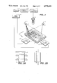
FIG. 1 is a block diagram of an apparatus embodying the present invention,
FIGS. 2A and 2B are examples of slit line patterns formed by slit line beams on a mounted circuit board,
FIG. 3 is a plan view of a mounted circuit board partitioned into areas for inspection according to a method embodying the present invention,
FIG. 4 is a plan view of one of the partitioned areas shown in FIG. 3,
FIGS. 5A-5C are plan views of slit line patterns by a component mounted on a circuit board,
FIGS. 6A-6C are plan views of windows used in an inspection method of the present invention,
FIG. 7 is a flow chart showing an inspection method embodying the present invention,
FIGS. 8A and 8B are drawings for showing a method of determining an end point of a slit line image,
FIGS. 9, 10A and 10B are examples of slit line image,
FIG. 11A is a side view of a component soldered onto a circuit board and FIG. 11B is a slit line pattern obtained from the soldered component shown in FIG. 11A,
FIGS. 12A and 12B are examples of stored image data corresponding to a portion of the pattern shown in FIG. 11B,
FIG. 13 is a block diagram of another apparatus embodying the present invention of the type shown in FIG. 1 with portions thereof shown more in detail,
FIG. 14 is a flow chart showing portions of FIG. 7 more in detail,
FIGS. 15, 16 and 17 are drawings for showing the concept of and a method of using frames in an inspection method embodying the present invention,
FIG. 18 is a schematic drawing of a light source unit embodying the present invention,
FIGS. 19A and 19B are drawings for showing slit line patterns before and after the projection angle is changed by the system shown in FIG. 18,
FIG. 20 is a block diagram of another apparatus embodying the present invention of the type shown in FIGS. 1 and 13 with some portions thereof shown more in detail,
FIG. 21 is a schematic drawing of a shutter system embodying the present invention,
FIG. 22 is a front view of the disk shown in FIG. 21,
FIG. 23 is a schematic plan view of the position sensor shown in FIG. 21,
FIG. 24 is a schematic side view of the position sensor of FIGS. 21 and 23,
FIG. 25 is a schematic drawing showing positional relationships of the disk and the position sensor of FIG. 21 with respect to the light paths from the light sources,
FIG. 26 is a flow chart showing the operation of the shutter system of FIG. 21,
FIG. 27 is a signal waveform chart for the operation by a method according to the present invention,
FIGS. 28A-28E are schematic plan views for showing positional relationships between the angular orientation of the disk and the light paths,
FIG. 29 is a plan view of a prior art iris-type mechanical lens shutter, and
FIG. 30 is a signal wave form chart associated with a prior art shutter system.
In all these figures, components which are substantially identical or at least similar to each other are indicated for convenience by the same alphanumeric symbols.
DETAILED DESCRIPTION OF THE INVENTION
In what follows, the present invention is described by way of an example. With reference firstly to FIG. 1, a printed circuit board 3 with chip components 5 mounted thereon is placed on top of a table 4 which is freely movable two-dimensionally in X- and Y-directions as shown. For projecting lattice-like light lines on the surface of the printed circuit board 3, two sources of slit light beams 1X and 2Y respectively for the direction of the X-axis and the Y-axis are placed diagonally above the table 4. Each of these light sources 1X and 1Y is provided with a shutter 2X or 2Y such that line beams in the X- and Y-directions can be selectably and separately made incident on the mounted chip components 5 by controlling these shutters 2X and 2Y. An image receiving device 6 such as a camera is disposed above the printed circuit board 3 for receiving an image of the target objects as well as of their surroundings. An analog-to-digital (A/D) converter 7, an image processing device 8 to be described below more in detail and a control circuit 9 are serially connected to this image receiving device 6. The control circuit 9 is also connected to a table driving circuit 10 for moving the table 4 so as to control its motion through an X-direction driver 11X and a Y-direction driver 11Y.
More in detail, the X- and Y- direction drivers 11X and 11Y are operated by a signal transmitted from the control circuit 9 to the table driving circuit 10 such that those of the mounted chip components 5 on the printed circuit board 3 to be inspected come within the viewing range of the image receiving device 6. First, the shutter 2X on the X-direction light line source 1X is operated to project lines of light in the X-direction on these target components 5 and the slit pattern image obtained thereby is viewed from above by the image receiving device 6. Next, the shutter 2Y on the Y-direction light line source 1Y is operated to project lines of light in the Y-direction and the slit pattern image thus obtained is similarly viewed by the image receiving device 6. Image data corresponding to these pattern images are converted into a digital signal by the analog-to-digital converter 7.
Since the chip components 5 on the printed circuit board 3 are three-dimensional objects, the image of the light lines change according to their three-dimensional shapes. Near the outer peripheries of a viewing range, in particular, the image of the light lines become discontinuous, making it possible to detect the shape of these chip components 5. Thus, the digitally converted data are transmitted to the image processing device 8 where detection, calculation and judging circuits cooperate to detect the edges of the slit lines, calculate characteristic values of various kinds and eventually evaluate on the basis of such values whether the chip components 5 under investigation are properly mounted. The same procedure is repeated after the table 4 is moved and the conditions of all chip components 5 on the printed circuit board 3 can be inspected in this manner.
FIGS. 2A and 2B show examples of slit patterns projected on a chip component. Since the slit lines in the X-direction (FIG. 2A) and the Y-direction (FIG. 2B) are separately projected, each slit line can be inspected without interference from lines in the transverse direction and the edges (indicated by (1)-(6)) of the component 5 can be accurately determined. Although use of shutters was disclosed above for projecting slit lines in the X- and Y-directions, this is not intended to limit the scope of the present invention. Instead, strobes and switches may be used to emit light beams at desired time intervals to obtain desired slit images. Moreover, the slit light lines may be bright or dark lines.
Next, a method of inspection by using the apparatus described above is explained by way of the flow chart shown in FIG. 7. Initially, data related to individual chip components such as their positions, external dimensions, orientations and kinds are stored in the memory device of the image processing device 8. These data are stored in the order in which they are to be inspected and may be either created automatically or registered manually. In the "automatic creation mode", the data available from the time when the printed circuit board was designed or the data on a device carrying the chip components of interest transmitted to the inspection apparatus through telecommunication lines or by means of a floppy disk and the circuit board to be inspected is divided into areas to be viewed on the basis of these transmitted data. In the case of a circuit board 3 shown in FIG. 3, for example, four areas 3-1, 3-2, 3-3 and 3-4 each surrounded by broken lines may be sequentially viewed for the inspection of chips therein. Thereafter, the order in which the chips in each of the areas are to be inspected is determined. The three chips in Area 3-1 of FIG. 3 may be inspected in the order of 4-1, 4-2 and 4-3 as shown in FIG. 4. Data are stored in the memory in this order. In the "manual registration mode", use is made of an input device such as a mouse or a keyboard to effect the same procedure.
After these data have been stored, the printed circuit board 3 to be inspected is set on the table 4 and the inspection is started. The apparatus makes references to data and causes the table 4 to move such that the area to be viewed comes directly under the camera 6. When the target area comes directly under the camera 6, the shutters 2X and 2Y of the light sources 1X and 1Y are controlled such that slit lines are projected separately in the X- and Y-directions. Each time, image data received by the camera 6 are transmitted through the analog-to-digital converter 7 to the image processing device 8 and stored in the image memory device. As soon as these data are received, the table 4 starts moving to the next position while the received data are analyzed as will be explained below to determine whether the chips in the viewed area are properly mounted. This serves to improve the overall speed of inspection.
In the case of a chip component shaped as shown in FIG. 5A, for example, its slit images inputted by light lines in the X- and Y-directions may be as shown in FIGS. 5B and 5C, respectively, where eL1 -eL3 are the X-coordinates of the left-hand ends of slit light beams in the X-direction, eR1 -eR3 are those of their right-hand ends, eU1 -eU3 are the Y-coordinates of the upper ends of the slit light beams in the Y-direction and eD1 -eD3 are those of their lower ends, respectively. From such input images, "windows" are set for each chip to be inspected on the basis of the stored data thereon, the size of the windows being determined by the detected positional displacement and the external dimensions of the chip component. In the case of a standard chip component with no positional displacement, windows are generated as shown in FIGS. 6A-6C. If the coordinates of the center point of the standard chip component are (a,b), its external dimensions are (X,Y), the standard deviations thereof are (ΔX,ΔY) and the detected positional displacements are (mx, xy, the coordinates of the center of Window W1 shown in FIG. 6B are O1 (a-X/2, b), its length in the X-direction is 2(ΔX+mx) and its length in the Y-direction is 2(ΔY+my)+Y; the coordinates of the center of Window W2 shown in FIG. 6B are O2 (a+X/2, b), its length in the X-direction is 2(ΔX+mx) and its length in the Y-direction is 2(ΔY+my)+Y; the coordinates of the center point of Window W3 shown in FIG. 6C are O3 (a,b-Y/2), its length in the X-direction is 2(ΔX+mx)+X and its length in the Y-direction is 2(ΔY+my); and the coordinates of the center point of Window W4 shown in FIG. 6C are O4 (a,b+Y/2), its length in the X-direction is 2(ΔX+mx)+X and its length in the Y-direction is 2(Y+my).
After the windows are thus set, inspection is carried out according to the following algorithm. Firstly, threshold values are set for distinguishing between slit light beams and the background. They are set for each chip and separately for the X- and Y-directions. Next, these threshold values are used to detect slit lines and to determine the coordinates of their end points. If the end points are not within the corresponding windows, it is concluded that this chip component is not properly mounted and hence that the circuit board is defective. Only those of the detected slit light beams which serve to show the size of a chip component are kept and the rest are excluded. This is done by examining whether the condition (X-ΔX)≦(eR -eL)≦(X+ΔX) or (Y-ΔY)≦(eU -eD)≦(Y+ΔY) is satisfied regarding the length of a slit beam on a chip and whether the conditions eLX ≦eX ≦eRX and eDX ≦eY ≦eUX are satisfied where eL =(eLX, eY), eR =(e.sub. RX, eY), eU =(eX, eUY) and eD =(eX, eDY) are two-dimensional coordinates of the left-hand, upper and lower end points of slit light beams which cross each other. If there are not slit light beams satisfying these conditions, the chip component is considered defective.
If the slit light beam pattern for a chip component is as shown in FIGS. 5B and 5C, the coordinates of its center is obtained by the formulas CX =(eLX +eRX)/2 and CY =(eUY +eDY)/2 where the symbols on the right-hand sides of the equations indicate averages over the slit lines. The values of CX and CY thus calculated are compared with the corresponding data initially stored in the memory device and if either of the differences is greater than the corresponding threshold value, the chip is considered unacceptably displaced.
As shown in the flow chart of FIG. 7, retry routines are provided for chips which cannot be judged by the procedure explained above. Examples of retry routines to be provided include one for the case of a chip with halation and one for the case of a slit line which is totally broken up due to peculiar surface conditions of the chip. If retry routines are carried out for particular chip areas after the regular routine is completed, the algorithm can be simplified and the inspection can be carried out more efficiently. It also goes without saying that many variations of the above are to be considered within the scope of the present invention. For example defects and displacements may be detected by comparing the size of the standard chip (X,Y) and the lengths of the light beams (eR -eL, eU -eD). The apparatus of FIG. 1 may be modified such that the table 4 remains stationary and the camera 6 is moved. The inspection device described above need not be independently provided but may be incorporated in a device carrying electronic components.
Next, a method of tracing the center of a slit line beam is explained by way of an example and with reference initially to FIGS. 8A-8C which show a situation where an image received by the camera 6 of FIG. 1 has been converted into 256 digital data by the analog-to-digital converter 7 and these converted data have been stored in a RAM within the image processing device 8. In FIG. 8A, y0 --y0, indicates a starting line for inspection of a slit image 13. This is scanned and an initial threshold value Th0 is determined by a known method such as the so-called "P-tile" method. This threshold value is used to detect the width Sw of this slit image 13 and its center S0 also is determined. In the meantime, it is constantly being ascertained that the line y0 --y0 ' does across the slip image 13 under inspection. Next, this center point S0 is used as the starting point and an inspection window 14 with the size of m×n pixels is set as shown (m=3 and n=4 in FIGS. 8A-8C for convenience). These pixels correspond to memory elements of the RAM.
Next, brightness (or luminosity) values L0n -Lmn of the pixels P0n -Pmn on the right-hand edge of this window are examined and, if any of them exceeds the threshold value Th0, it is determined that there is a slit and a line y1 --y1, is set over the pixels P0n -Pmn (of FIG. 8A). The routine explained above is repeated next with reference to this newly set line y1 --y1 ' as shown in FIG. 8B. At the same time, a new threshold value Th1 is selected. As this routine is further repeated, the window thus set eventually reaches the right-hand end point of the slit line. FIG. 8C shows this situation wherein the luminosity values L0n -Lmn along the right-hand edge of the window 14 are all below the threshold value Thi at this moment, i indicating the number of repetitions which have brought the window 14 to this position from the initial position shown in FIG. 8A. These low luminosity values now indicate that the right-hand end point of the slit line is inside this window 14 (of FIG. 8C) and a search for the exact location of the end point is continued from the left-hand edge along the pixels P00 -P0n one column at a time. When a column (the jth) is reached such that the luminosity values of all pixels P0j -Pmj on this column are below the threshold value Thi, it is considered the true right-hand end point.
With the tracing method of the present invention explained above, end points of slit lines can be efficiently and accurately determined even if there are large variations in the luminosity of the image. Even if the widths of a slit line changes as shown in FIG. 9, such changes do not affect the accuracy of the method. In the case of a small gap in a slit line as shown in FIGS. 10A and 10B, the end points can be still correctly identified if the inspection routine is slightly modified such that the window is advanced one step further after an end point of a slit line is tentatively detected as shown in FIG. 10A. If the slit is detected again at this advanced position shown in FIG. 10B, it is considered that the gap detected in the position of FIG. 10A does not really represent the end point and the window is further advanced to the right-hand side as explained above. If no slit image s detected at the advanced window position (unlike FIG. 10B), the end point detected (in FIG. 10A) before the window was advanced is considered the true end point.
Another advantage of the tracing method of the present invention is appreciated with reference to FIGS. 11A and 11B. When a chip component 16 is soldered as shown in FIG. 11A wherein numeral 15 indicates solder, the slit light line thereon may become diagonal as shown in FIG. 11B because of sloped solder surfaces. The width of a slit line may further fail to remain constant. By the method of the present invention, however, the same end point can be accurately identified. If the slit width is D and the window width is W and if the slit bends by θ as shown in FIG. 12A or 12B, say, due to a sloped solder surface as shown in FIG. 10A, the detection error Le is (D+W)/(2tanθ) in both cases.
In the case of slits with large fluctuations in brightness, the value of n for the windows should be reduced. If the fluctuations are small, n may be made large to reduce the time required for determining end points.
In connection with the method and apparatus of the present invention, for example, as shown and described above by way of FIG. 1, a method of preparing the data to be initially stored in the image processing device 8 is described next in detail.
As shown in FIG. 13 which describes portions of FIG. 1 more in detail, a printed circuit board 3 with chip components 41-46 such as semiconductor elements, capacitors and resistors mounted thereon is secured to a base plate 19 of a table (or a so-called XY table) 4 which is comprised not only of the base plate 19 but also of an X-direction and Y-direction control means 11X and 11Y so as to be able to move the printed circuit board 3 two-dimensionally along a mutually perpendicular set of axes X and Y. Above the printed circuit board 3 are an image receiving device 6 and light sources 1X and 1Y. The image receiving device 6 is connected to detecting means 24 for detecting mounted positions of components based on data signals outputted from the image receiving device 6.
The detecting means 24 is also connected to input means 26 through a computer 25. The input means 26 may comprise a keyboard, a floppy disk driving device, ports for data communication, etc. such that a series of data inclusive of the sizes, positions, orientations, etc. of the mounted chip components 41-46, their maximum allowed displacements, etc. may be inputted therethrough. The computer 25 is designed to serve as a combination of means for determining viewing positions for the image receiving device 6 such that those of the chip components to be inspected can be viewed, means for determining for each viewing position of the image receiving device 22 allowable ranges of positions for viewable chip components, means for comparing the positions of the chip components 41-46 detected by the detecting means 24 with the allowable ranges of their positions and means for determining a sequence according to which the image receiving device 6 is to be moved from one to another of the viewing positions. The computer 25 is also connected to a table control means 10 for controlling the table 4.
Before the mounted conditions of the chip components 41-46 are inspected by the apparatus thus structured, various data as explained above by way of FIG. 7 are inputted through the input means 26 as shown also in FIG. 14 (at S1) which is another flow chart showing portions of FIG. 7 more in detail. Next, frames 41'-46' are defined to serve as boundaries of allowable ranges of positions of the individual chip components 41-46 (S2). A method of defining a frame according to the present invention for this purpose is explained next by way of FIG. 15 wherein the component 41 is illustrated as having a size indicated by X and Y. If the maximum allowable positioning error regarding this component 41 is SX and SY respectively in the X- and Y-directions, the size of its frame 41' is given by LX=X+2SX and LY=Y+2SY.
After frames 41'-46' are thus calculated respectively for the chip components 41-46, the surface of the circuit board 3 is partitioned in the direction of the Y axis as shown in FIG. 16 into n blocks 34 of width D each (S3). If the area 31 on the circuit board 3 viewable from a single viewing position by the image receiving device 6 is CX×CY, D is selected to be smaller than CY. Next, viewing areas 31-33 on the circuit board 3 are set for each of the blocks 34 (S4). In the case of the chip components 41-43 contained in the first of the blocks 34 and having frames 41'-43' as shown in FIG. 17, for example, a first viewing area 31 is so selected that the frame or frames with the smallest X-coordinate and the smallest Y-coordinate (the frame 41' as both in this example) will be at the left-hand edge and the bottom, respectively. After such a viewing area is determined, the chip components of which the frames are completely contained therein are assigned numbers ascendingly to represent their viewing sequence. In FIG. 17, two (41 and 42) of the chip components 41-43 have their frames completely within this viewing area 31 and are therefore numbered "1" and "2", respectively. For the third chip component 43, another viewing area 32 is set similarly with respect to its frame 43' as shown in FIG. 13 and is numbered "3". After the viewing sequence of all components within a block is completed, the same routine is repeated for the next one of the blocks 34.
After the viewing areas 31-33 are thus determined, maximum allowable ranges of positions 35-40 respectively for the chip components 41-46 are determined (S5) for each of the vieWing areas 31-33 on the basis of the mounted positions of the chip components 41-46 on the circuit board 3, their frames 41'-46' and the viewing areas 31-33. Additionally, the distances by which the table 4 must be moved such that each of the viewing areas 31-33 can be viewed by the image receiving device 6 are also calculated. The sequence of tab)e motions is determined at this moment such that the frequency of movements by the table 4 and the distance to be traveled are minimized (S6).
Thereafter, the table 4 is moved according to the results of calculations obtained in Step S6. At each table position, image data from the corresponding one of the viewing areas 31-33 are received by the image receiving device 6. Image data of all chip components 41-46 are thus received and stored in a memory device of the computer 25. The positions of the individual chip components 41-46 are detected on the basis of these data and a final determination whether the printed circuit board 3 is defective or not is made as explained above by way of FIG. 7. Although a single computer was disclosed at 25 in FIG. 13 for both preparing data and for carrying out inspections but this is not intended to limit the scope of the present invention. A plurality of computers may be employed for their separate functions.
Next, the slit light sources 1X and 1Y of FIG. 1 and FIG. 13 are described more in detail. As shown in FIG. 18, light energy emitted from a source 47 such as a halogen lamp is passed through a condenser lens 48 or the like to form a parallel beam in order to improve the illumination efficiency and made incident uniformly onto a slit screen 49. Although not illustrated in the figure, this slit screen 49 comprises a glass plate with vapor-deposited chromium thereon and there are 63 slits of 15 μm in width formed thereon at a pitch of 400 μm. Thus, the parallel beam of light from the condenser lens 48 appears, after passing through this slit screen 49, as slit light beams. (Only five of these slit light beams 53-57 are shown in FIG. 18 for convenience.) The slit light beams 53-57 thus generated are thereafter passed through a focusing lens 50 and reflected by a mirror 51 subsequentially to be projected onto a selected area of the printed circuit board 3. In FIG. 18, numeral 58 indicates a box for this optical unit containing the source lamp 47, the lenses 48 and 50 and the slit screen 49.
More in detail, the slit light beams 53-57 passing through the focusing lens 50 are reflected by the mirror 51 connected to an angle control device 52 for adjusting the angle of incidence of these beams 53-57. The angle θ made between these beams 53-57 and the surface of the printed circuit board 3 will be hereinafter referred to as the projection angle. The aforementioned angle control device 52 is essentially a servo mechanism comprised of an actuator or the like for varying the angle of the mirror 51. A retractable arm is attached to an edge on the backside of the mirror 51 such that the projection angle θ can be adjustably varied. In FIG. 18, dotted lines indicate how the projection angle θ may be changed by changing the angle of the mirror 51.
FIGS. 19A and 19B show how detectability of a three-dimensional chip components 5 mounted on the circuit board 3 can be affected by the projection angle θ. FIG. 19A shows a situation where the slit light images projected on the circuit board 3 and the mounted component 5 are apparently continuous and hence the component 5 cannot be detected. If the projection angle is changed from θ, say to θ1 as shown in FIG. 18, the slit line images can be relatively displaced as shown in FIG. 19B such that the chip components 5 on the circuit board 3 can be made detectable.
Functional relationship between the slit light source shown in FIG. 18 and an apparatus of the type shown schematically in FIGS. 1 and 13 is shown in FIG. 20 wherein the optical unit boxes for the light sources 1X and 1Y are separately shown at 58X and 58Y as well as their associated mirrors 51X and 51Y and their angle control devices 52X and 52Y. Various controlling means such as mirror angle control means 62 and shutter control means 63 in addition to the table controller 10 are separately illustrated for the purpose of explanation.
Commands for moving the table 4 are transmitted through the table controller 10 to the X- and Y- direction table drivers 11X and 11Y such that the first viewing area on the circuit board 3 can be viewed through the image receiving device 6. Next, the lamps in both optical unit boxes 58X and 58Y are switched on and a command is transmitted to the shutter controller 63 such that shutters for light sources in the two boxes 58X and 58Y are alternately operated. As a result, slit line images in the X- and Y-directions are alternately projected on the circuit board 3 and these images are received by the image receiving device 6 and sequentially stored in the memory device for he control device 9 (shown separately at 61 in FIG. 20). If slit line images either in the X-direction or the Y-direction overlap as shown in FIG. 19A such that one of the components 5 on the circuit board 3 cannot be detected, a command is transmitted through the mirror angle controller 62 to cause the corresponding angle control device 52X or 52Y to change the angle of the associated mirror 51X of 51Y to thereby change the projection angle θ as explained above such that the overlapping of slit line images is removed and the hitherto undetectable component 5 becomes detectable. In other words, since commands for operating the angle control devices 52X and 52Y which form servo mechanisms correspond to the projection angles (both in the X- and Y-directions), the control unit 9 has a record of these projection angles and hence is capable of examining chip components 5 on the basis of these projection angles and the corresponding distance of separation P shown in FIG. 19B.
Mechanisms embodying the present invention for the aforementioned shutters are explained next by way primarily of FIG. 21. As mentioned above, shutters are used in the apparatus embodying the present invention for quickly switching the projection of light beams in the X- and Y-directions. Prior art technologies for this purpose included devices using iris-type mechanical lens shutters as shown in FIG. 29, liquid crystal elements, ceramic elements or strobe light sources. Iris-type mechanical lens shutters are disadvantageous because they include many parts which operate in complicated manners and hence cannot operate quickly and do not last long. As for high-speed shutters relying on a liquid crystal or a ceramic element, the amount of transmitted light varies significantly, depending on changes in temperature. They are therefore not easy to use near a heat-emitter such as a light source. Devices using a xenon light-emitter of the type satisfactory regarding both brightness and lifetime are too expensive to be practical.
With reference to FIG. 21 which shows a shutter system according to the present invention, numeral 73 indicates a disk to be described more fully below, numeral 74 indicates a rotary position sensor, numeral 75 indicates a signal generation circuit, numeral 81 indicates a motor for rotating the disk 73 and numeral 82 indicates a mechanism for controlling the rotary motion of the disk 73. As explained above in connection with FIGS. 1, 13 and 20, the light sources 1X and 1Y are so adapted as to transmit slit light beams which cross each other perpendicularly to each other somewhere on a plane parallel to the target surface (represented in FIG. 21 by that of the printed circuit board 3) and closer to the image receiving device 6 before projecting slit line images respectively in the X- and Y-directions on that target surface. The disk 73 is rotatably supported at a position where it blocks by crossing both light paths 80X and 80Y respectively from the light sources 1X and 1Y to the target surface. The rotary position sensor 74 may be of any known kind and is adapted to detect the angular position of the disk 73.
The signal generation circuit 75 is adapted to output vertical and horizontal external synchronization signals to the image receiving device 6 according to the rotary orientation of the disk 73 as detected by the sensor 74. The control unit 9 performs various operations, as explained above, upon receiving image data through the image receiving device 6. When a signal from this control unit 9 has been received, the signal generation circuit 75 waits for a predetermined length of time TA after a signal from the position sensor 74 is received and transmits a vertical synchronization signal. The image receiving device is adapted not only to receive image data from the target surface, but also to retain the image data for a predetermined time interval. Alternatively, the operation of the image receiving device 6 may be externally controlled, for example, by vertical synchronizing video signals (vertical drive VD).
The rotatably supported disk 73 is provided with a shutter window 84 shaped as shown in FIG. 22 like a fan with rims which are coaxial to the circular periphery of the disk 73 itself. Areas 85 and 86 surrounded by dotted elliptical lines in FIG. 22 schematically indicate cross sections of slit light beams 80X and 80Y respectively from the light sources 1X and 1Y as they cross the disk 73. As the disk 73 is rotated around its axis of symmetry, the light paths 80X and 80Y are therefore alternately blocked. The disk 73 is rotated at a rate of about 900rpm. Of the video signal from the image receiving device 6, the vertical synchronizing signal has a frequency of about 33.4 milliseconds per field. Thus, the disk 73 makes about 0.5 rotations at this frequency.
The rotary position sensor 74 may be structured as shown in FIGS. 23 and 24 with a detector disk 87 disposed coaxially and affixed so as to rotate with the disk 73 of which the orientation is to be detected. An opening 90 is formed at a point near the outer periphery of this detector disk 87 and two photoswitches 88 and 89 are disposed near its periphery and diametrically opposite to each other. As the detector disk 87 rotates, the opening 90 also rotates and a signal is outputted whenever this opening 90 passes the position of either one of these photoswitches 88 and 89.
The positional relationships of the disk 73 and the position sensor 74 with respect to the light paths 80X and 80Y which cross each other perpendicularly to each other are shown in FIG. 25. As explained above in connection with FIG. 21, the disk 73 is so positioned as to cross both of these light paths 80X and 80Y. Thus, as the disk 73 rotates and its shutter window 84 comes to the position crossed by the light path 80X, the slit light beam along this path 80X is allowed to pass through and reflected by the mirror 51X to project slit line images in the X-direction. At this moment, the other light path 80Y is blocked by the disk 73 and no slit light beam can reach the target surface to project thereon any slit line images in the Y-direction. After the disk 73 makes a half revolution and when the shutter window 84 comes to the position where the slit light beam 80Y crosses the disk 73, the beam is allowed to pass through to the mirror 51Y, is reflected thereby and projects slit line images in the Y-direction. At this moment, the other light path 80X is blocked by the disk 73 and no slit light beam can reach the target surface to project thereon any slit line images in the X-direction.
Operation of the shutter system described above is explained next by way of the flow chart shown in FIG. 26 and the timing chart shown in FIG. 27. As explained above and shown in FIG. 27, the two photoswitches 88 and 89 of the position sensor 74 (Sensor X and Sensor Y) transmit signals alternately. When one of such sensor signals S is received (#1), it is determined which of the light paths 80X and 80Y is open (#2) and image data are accumulated by the image receiving device 6 during one field period. Depending upon whether slit line images along the X-or Y-direction have been received, the received image data are stored either in areas for vertical (V) image data (#3) or in areas for horizontal (H) image data (#7) within the memory device 61. When the storage period comes to an end, a termination signal is outputted (#4 or #8) and image data from slit light image in the other direction are received (#5 or #9). At this moment, image data from slit light images in both X- and Y-directions are stored in the memory device 61. When a second termination signal is outputted from the memory (#6 or #10) to thereafter indicate the end of another storage period, the control unit 9 begins to process the stored image data (#12) as explained above. At the same time, the system begins to wait for the next input of a signal from the position sensor 74 and when a signal is received from the position sensor 74 (#15), the system waits for a predetermined period of time TA as explained above and the signal generation circuit 75 retransmits a video synchronizing signal (#16). Although this restarting of a video synchronizing signal is restricted by the rotation of the motor 81, the motor 81 has only to be started once if a high-accuracy motor is used. Since motors with high rotary accuracy are expensive, a preferable method is to use an inexpensive motor and to increase the number of starts. FIGS. 28A-28E show the angular positions of the disks 73 at various moments I, II, III, IV and V in the cycle of its operation shown in FIG. 27. The timing chart of FIG. 27 should be compared with a corresponding chart for a prior art system using an ires-type mechanical lens shutter. The comparison clearly shows that the shutter system of the present invention is much speedier.

Claims (10)

What is claimed is:
1. An apparatus for inspecting components mounted on a circuit board comprising
light source means for causing a plurality of slit light beams to be made incident on a circuit board diagonally from above, said light source means including a first source unit for projecting slit light images in a first direction on said circuit board and a second source unit for projecting slit light images in a second direction on said circuit board, said first and second directions being different,
image receiving means for receiving said slit pattern images formed on said circuit board, and
image processing means for generating data on positions of components mounted on said circuit board by receiving image signals from said image receiving means.
2. The apparatus of claim 1 further comprising
input means for receiving a series of input data inclusive of fields of vision of said image receiving means, sizes, positions and orientations of said mounted components on said circuit board and maximum allowable positional errors,
means for determining viewing positions at which said image receiving means is to be set above said circuit board such that target components to be inspected are viewable by said image receiving means,
means for determining for each one of said viewing positions allowable positional ranges for those of said target components viewable by said image receiving means from said one of said viewing positions, and
means for determining a sequence in which said image receiving means is moved from one to another of said viewing positions.
3. The apparatus of claim 1 wherein said light source means include a first source unit for projecting slit light images in a first direction on said circuit board and a second source unit for projecting slit light images in a second direction on said circuit, said first and second directions being different, each of said source units being comprised of
a light emitter,
a slit screen for receiving light from said light emitter and transmitting a plurality of mutually parallel slit light beams,
a mirror for reflecting said plurality of slit light beams to direct said slit light beams to said circuit board, and
means for adjustably varying the orientation of said mirror for changing the projection angle at which said slit light beams are projected onto said circuit board.
4. The apparatus of claim 3 wherein each of said source units is further comprised of
a converging lens disposed between said light emitter and said slit screen to project a beam of light from said light emitter onto said slit screen, and
a focusing lens disposed between said slit screen and said mirror to focus said slit light beams on said circuit board.
5. The apparatus of claim 3 wherein said first and second directions of substantially perpendicular to each other.
6. The apparatus of claim 1 wherein said light source means include a first source unit for emitting slit light beams along a first light path to project slit light images in a first direction on said circuit board and a second source unit for emitting slit light beams along a second light path to project slit light images in a second direction on said circuit board, said first and second directions being different, and wherein said switching means include
a disk having a window and rotatably supported at a position crossed by both said first and second light paths,
a position sensor for detecting angular position of said window with respect to said disk as said disk rotates, and
signal generation means for responding to a position signal received from said position sensor by transmitting a command signal to said image receiving means to cause said image receiving means to receive image data from said circuit board when said slit light images in said first or second direction are projected on said circuit board.
7. A method of inspecting whether components are correctly mounted on a circuit board comprising the steps of
exposing said mounted circuit board to a plurality of slit line beams from light source means and made incident diagonally from above by switching said light source means on and off,
receiving image data of said mounted circuit board when slit line images are projected on said mounted circuit board by said slit line beams,
defining frames on said circuit board with respect to intended positions of said components,
determining actual positions of said components by analyzing said image data, and
determining whether said components are properly mounted or not by comparing said detected actual positions and positions of said frames.
8. The method of claim 7 further comprising the step of storing said image data, said step of determining actual component position including the steps of
selecting with reference to said stored image data a center point of one of said slit line images,
considering an inspection area including said center point near one edge thereof,
setting a threshold value regarding brightness of image,
making a comparison between brightness of image at the opposite edge of said inspection area and said threshold value, and
identifying an edge position of one of said components from the results of said comparison.
9. The method of claim 7 wherein said slit line beams are projected onto said circuit board in two directions which are substantially perpendicular to each other.
10. The method of claim 9 wherein said slit line beams projected into said two different directions are projected alternately.
US07/218,311 1987-07-14 1988-07-12 Method of and apparatus for inspecting mounting of chip components Expired - Fee Related US4978224A (en)

Applications Claiming Priority (10)

Application Number Priority Date Filing Date Title
JP62-175224 1987-07-14
JP62175224A JPS6418004A (en) 1987-07-14 1987-07-14 Center tracking of slit light
JP62175225A JPS6418049A (en) 1987-07-14 1987-07-14 Inspection for mounting of chip part
JP62-175225 1987-07-14
JP24665787A JPS6488204A (en) 1987-09-30 1987-09-30 Apparatus for inspecting part mounting state
JP62-246657 1987-09-30
JP62-322086 1987-12-18
JP32208687A JPH01161310A (en) 1987-12-18 1987-12-18 Two-light source rapid switching shutter device for image processing
JP62-326061 1987-12-22
JP32606187A JPH01165903A (en) 1987-12-22 1987-12-22 Slit light beam source apparatus

Publications (1)

Publication Number Publication Date
US4978224A true US4978224A (en) 1990-12-18

Family

ID=27528631

Family Applications (1)

Application Number Title Priority Date Filing Date
US07/218,311 Expired - Fee Related US4978224A (en) 1987-07-14 1988-07-12 Method of and apparatus for inspecting mounting of chip components

Country Status (1)

Country Link
US (1) US4978224A (en)

Cited By (69)

* Cited by examiner, † Cited by third party
Publication number Priority date Publication date Assignee Title
US5076697A (en) * 1987-10-14 1991-12-31 Hitachi, Ltd. Apparatus and method for inspecting defect of mounted component with slit light
EP0526080A2 (en) * 1991-07-22 1993-02-03 Omron Corporation Teaching method and system for mounted component inspection
US5329359A (en) * 1991-05-17 1994-07-12 Canon Kabushiki Kaisha Parts mounting inspection method
US5390131A (en) * 1992-04-06 1995-02-14 Hewlett-Packard Company Apparatus and method for displaying wafer test results in real time
US5598345A (en) * 1990-11-29 1997-01-28 Matsushita Electric Industrial Co., Ltd. Method and apparatus for inspecting solder portions
US5648853A (en) * 1993-12-09 1997-07-15 Robotic Vision Systems, Inc. System for inspecting pin grid arrays
US5663569A (en) * 1993-10-14 1997-09-02 Nikon Corporation Defect inspection method and apparatus, and defect display method
US5691544A (en) * 1992-06-24 1997-11-25 Robotic Vision Systems, Inc. Apparatus for obtaining three-dimensional data from multiple parts or devices in a multi-pocketed tray
US5729895A (en) * 1994-12-28 1998-03-24 Daewoo Electronics Co., Ltd. Process for compensating for the position of a camera in a chip mount system and process for mounting chips using the compensation method
GB2317447A (en) * 1996-09-24 1998-03-25 Daewoo Electronics Co Ltd PCB inspection system
US5778177A (en) * 1994-09-28 1998-07-07 At&T Corp. Interactive scanning device or system
US5793051A (en) * 1995-06-07 1998-08-11 Robotic Vision Systems, Inc. Method for obtaining three-dimensional data from semiconductor devices in a row/column array and control of manufacturing of same with data to eliminate manufacturing errors
EP0935135A1 (en) * 1998-02-09 1999-08-11 MV Research Limited System for measuring solder bumps
US5984493A (en) * 1997-04-14 1999-11-16 Lucent Technologies Inc. Illumination system and method
US5995232A (en) * 1997-07-14 1999-11-30 U.S. Philips Corporation Method of and device for inspecting a PCB
US6023569A (en) * 1996-06-29 2000-02-08 Daewoo Electronics Co., Ltd. Method and device for producing automatic insertion path in apparatus for automatically inserting electronic components into printed circuit board
US6043877A (en) * 1996-11-26 2000-03-28 U.S. Philips Corporation Calibration carrier for a component placement machine having an adhesive reflective surface
WO2000038494A2 (en) * 1998-12-19 2000-06-29 Cyberoptics Corporation Automatic inspection system with stereovision
US6088106A (en) * 1997-10-31 2000-07-11 Lap Gmbh Laser Applikationen Method for the contact-free measurement of the distance of an object according to the principle of laser triangulation
EP0959654A3 (en) * 1998-05-19 2000-08-09 FUJI MACHINE Mfg. Co., Ltd. Method and system for mounting electric components
EP1048946A3 (en) * 1999-04-27 2001-09-19 Matsushita Electric Industrial Co., Ltd. Inspection method and device
US20020136443A1 (en) * 2001-03-21 2002-09-26 Fuji Machine Mfg. Co., Ltd. Method and apparatus for detecting position of lead of electric component, and electric-component mounting method
US20020171847A1 (en) * 2001-04-27 2002-11-21 Tadashi Fukumoto Three-dimensional shape-measuring system
US20030020905A1 (en) * 2001-07-26 2003-01-30 Orbotech Ltd. Electrical circuit conductor inspection
US20030110610A1 (en) * 2001-11-13 2003-06-19 Duquette David W. Pick and place machine with component placement inspection
US20030131056A1 (en) * 2001-08-14 2003-07-10 Noriyuki Suzuki Method and system of distributing teaching data for image processing apparatus
US6614925B2 (en) * 1999-07-28 2003-09-02 Intelligent Reasoning Systems, Inc. System and method for performing basic training
US6655019B2 (en) * 1998-05-15 2003-12-02 Framatome Connectors International Device for aligning a printed circuit board in a press
US6665066B2 (en) * 2001-04-27 2003-12-16 National Instruments Corporation Machine vision system and method for analyzing illumination lines in an image to determine characteristics of an object being inspected
US20040146195A1 (en) * 2002-07-25 2004-07-29 Matsushita Electric Industrial Co., Ltd. Printing inspection apparatus, printing inspection method, printing inspection data generating apparatus, and printing inspection data generating method
US20040156539A1 (en) * 2003-02-10 2004-08-12 Asm Assembly Automation Ltd Inspecting an array of electronic components
WO2004086840A2 (en) * 2003-03-28 2004-10-07 Assembleon N.V. Method of placing at least one component on at least one substrate and apparatus therefore
US20040218040A1 (en) * 2003-01-24 2004-11-04 Yoshihiro Akiyama Appearance inspection apparatus and method of image capturing using the same
US6898333B1 (en) * 1999-08-06 2005-05-24 Cognex Corporation Methods and apparatus for determining the orientation of an object in an image
US20050276464A1 (en) * 2001-11-13 2005-12-15 Duquette David W Image analysis for pick and place machines with in situ component placement inspection
US20060002604A1 (en) * 2004-05-07 2006-01-05 Kaoru Sakai Method and apparatus for pattern inspection
US20060016066A1 (en) * 2004-07-21 2006-01-26 Cyberoptics Corporation Pick and place machine with improved inspection
KR100576392B1 (en) 2005-11-30 2006-05-03 기가비스주식회사 Apparatus for vision inspection
US20060197829A1 (en) * 2005-03-07 2006-09-07 Zanzucchi Peter J Reflection spectroscopic means for detecting patterned objects
US20070010969A1 (en) * 2003-11-07 2007-01-11 Cyberoptics Corporation Pick and place machine with improved setup and operation procedure
US20070276867A1 (en) * 2006-05-23 2007-11-29 David Fishbaine Embedded inspection image archival for electronics assembly machines
US7346420B2 (en) 2001-11-13 2008-03-18 Cyberoptics Corporation Component feeder exchange diagnostic tool
US7383152B1 (en) 2006-01-10 2008-06-03 Alliant Techsystems Inc. Non-contact deviation measurement system
WO2008086016A1 (en) * 2007-01-10 2008-07-17 Cyberoptics Corporation Inspection system
US7463352B2 (en) 1999-11-17 2008-12-09 Applied Materials, Inc. Method and apparatus for article inspection including speckle reduction
DE102004043084B4 (en) * 2003-09-12 2009-01-29 Oerlikon Assembly Equipment Ag, Steinhausen Device and method for mounting or wiring semiconductor chips
US20090110263A1 (en) * 2007-10-30 2009-04-30 The Testing Industry Benchmark Coplanarity inspection device for printed circuit boards
US7545514B2 (en) 2005-09-14 2009-06-09 Cyberoptics Corporation Pick and place machine with improved component pick image processing
US7559134B2 (en) 2003-11-04 2009-07-14 Cyberoptics Corporation Pick and place machine with improved component placement inspection
US20090198464A1 (en) * 2008-01-31 2009-08-06 Caterpillar Inc. System and method for assembly inspection
US20100045729A1 (en) * 2008-08-19 2010-02-25 Silverbrook Research Pty Ltd Method for testing alignment of a test bed with a plurality of integrated circuits thereon
US20100044437A1 (en) * 2008-08-19 2010-02-25 Silverbrook Research Pty Ltd Measuring apparatus for a carrier of printhead integrated circuitry
US20100046007A1 (en) * 2008-08-19 2010-02-25 Silverbrook Research Pty Ltd Measuring apparatus for performing positional analysis on an integrated circuit carrier
US20100045986A1 (en) * 2008-08-19 2010-02-25 Silverbrook Research Pty Ltd Imaging apparatus for imaging integrated circuits on an integrated circuit carrier
US7706595B2 (en) 2003-11-07 2010-04-27 Cyberoptics Corporation Pick and place machine with workpiece motion inspection
US20100321031A1 (en) * 2009-06-22 2010-12-23 Xerox Corporation Optical component identifier
US20110069154A1 (en) * 2009-09-22 2011-03-24 Case Steven K High speed, high resolution, three dimensional solar cell inspection system
US20110069878A1 (en) * 2009-09-22 2011-03-24 Case Steven K High speed optical inspection system with camera array and compact, integrated illuminator
US20110069507A1 (en) * 2009-09-22 2011-03-24 Haugan Carl E Dark field illuminator with large working area
US20110075137A1 (en) * 2007-12-19 2011-03-31 Hitachi High-Technologies Corporation Defect inspection system
US20110090333A1 (en) * 2009-09-22 2011-04-21 Haugan Carl E High speed optical inspection system with adaptive focusing
US20110102575A1 (en) * 2009-09-22 2011-05-05 Case Steven K High speed distributed optical sensor inspection system
US20110175997A1 (en) * 2008-01-23 2011-07-21 Cyberoptics Corporation High speed optical inspection system with multiple illumination imagery
US20110191050A1 (en) * 2010-02-01 2011-08-04 Koh Young Technology Inc. Method of inspecting a three dimensional shape
DE102006005874B4 (en) * 2005-05-11 2012-02-16 Hgv Vosseler Gmbh & Co. Kg Method for non-contact measurement
US20140036096A1 (en) * 2012-08-06 2014-02-06 Axis Ab Image sensor positioning apparatus and method
WO2015048892A1 (en) * 2013-10-01 2015-04-09 Sierra Wireless, Inc. Method and apparatus for electrical keying of an integrated circuit package having rotationally symmetric footprint
DE102005011330B4 (en) * 2005-03-12 2018-11-08 Pi4_Robotics Gmbh Method for detecting the position of a molded part
DE102007063932B4 (en) 2006-01-26 2023-11-02 Koh Young Technology Inc. Method for measuring a three-dimensional shape

Citations (4)

* Cited by examiner, † Cited by third party
Publication number Priority date Publication date Assignee Title
US4578810A (en) * 1983-08-08 1986-03-25 Itek Corporation System for printed circuit board defect detection
US4692690A (en) * 1983-12-26 1987-09-08 Hitachi, Ltd. Pattern detecting apparatus
US4728195A (en) * 1986-03-19 1988-03-01 Cognex Corporation Method for imaging printed circuit board component leads
US4799175A (en) * 1984-06-12 1989-01-17 Dainippon Screen Mfg., Co. System for inspecting pattern defects of printed wiring boards

Patent Citations (4)

* Cited by examiner, † Cited by third party
Publication number Priority date Publication date Assignee Title
US4578810A (en) * 1983-08-08 1986-03-25 Itek Corporation System for printed circuit board defect detection
US4692690A (en) * 1983-12-26 1987-09-08 Hitachi, Ltd. Pattern detecting apparatus
US4799175A (en) * 1984-06-12 1989-01-17 Dainippon Screen Mfg., Co. System for inspecting pattern defects of printed wiring boards
US4728195A (en) * 1986-03-19 1988-03-01 Cognex Corporation Method for imaging printed circuit board component leads

Non-Patent Citations (6)

* Cited by examiner, † Cited by third party
Title
Cheng; "Design for an Automated Recognition System for Multilayer Circuit Board Testing"; SPIE, vol. 255, Practical Electro-Optical Inst. and Techniques (1980) pp. 40-42.
Cheng; Design for an Automated Recognition System for Multilayer Circuit Board Testing ; SPIE, vol. 255, Practical Electro Optical Inst. and Techniques (1980) pp. 40 42. *
T. Masaki, et al., "Solder Inspection System for Surface Mount Board", Pros. Spring (1988) General Meeting Institute of Electronic Information and Communication Engineers, pp. 2-247.
T. Masaki, et al., Solder Inspection System for Surface Mount Board , Pros. Spring (1988) General Meeting Institute of Electronic Information and Communication Engineers, pp. 2 247. *
Y. Kakinoki, et al., "Loaded Printed Circuit Board Inspection with 3-D Measurement of Component Orientation", (Institute of Electronic Information and Communication Engineers), PRL85-34, pp. 67-75.
Y. Kakinoki, et al., Loaded Printed Circuit Board Inspection with 3 D Measurement of Component Orientation , (Institute of Electronic Information and Communication Engineers), PRL85 34, pp. 67 75. *

Cited By (119)

* Cited by examiner, † Cited by third party
Publication number Priority date Publication date Assignee Title
US5076697A (en) * 1987-10-14 1991-12-31 Hitachi, Ltd. Apparatus and method for inspecting defect of mounted component with slit light
US5598345A (en) * 1990-11-29 1997-01-28 Matsushita Electric Industrial Co., Ltd. Method and apparatus for inspecting solder portions
US5329359A (en) * 1991-05-17 1994-07-12 Canon Kabushiki Kaisha Parts mounting inspection method
EP0526080A2 (en) * 1991-07-22 1993-02-03 Omron Corporation Teaching method and system for mounted component inspection
EP0526080A3 (en) * 1991-07-22 1993-03-31 Omron Corporation Teaching method and system for mounted component inspection
US5822449A (en) * 1991-07-22 1998-10-13 Omron Corporation Teaching method and system for mounted component inspection
US5390131A (en) * 1992-04-06 1995-02-14 Hewlett-Packard Company Apparatus and method for displaying wafer test results in real time
US5691544A (en) * 1992-06-24 1997-11-25 Robotic Vision Systems, Inc. Apparatus for obtaining three-dimensional data from multiple parts or devices in a multi-pocketed tray
US5663569A (en) * 1993-10-14 1997-09-02 Nikon Corporation Defect inspection method and apparatus, and defect display method
US5648853A (en) * 1993-12-09 1997-07-15 Robotic Vision Systems, Inc. System for inspecting pin grid arrays
US5778177A (en) * 1994-09-28 1998-07-07 At&T Corp. Interactive scanning device or system
US5729895A (en) * 1994-12-28 1998-03-24 Daewoo Electronics Co., Ltd. Process for compensating for the position of a camera in a chip mount system and process for mounting chips using the compensation method
US5793051A (en) * 1995-06-07 1998-08-11 Robotic Vision Systems, Inc. Method for obtaining three-dimensional data from semiconductor devices in a row/column array and control of manufacturing of same with data to eliminate manufacturing errors
US6023569A (en) * 1996-06-29 2000-02-08 Daewoo Electronics Co., Ltd. Method and device for producing automatic insertion path in apparatus for automatically inserting electronic components into printed circuit board
GB2317447A (en) * 1996-09-24 1998-03-25 Daewoo Electronics Co Ltd PCB inspection system
GB2317447B (en) * 1996-09-24 2000-04-12 Daewoo Electronics Co Ltd Method and apparatus for inspecting inserting state of components in printed circuit board
US6043877A (en) * 1996-11-26 2000-03-28 U.S. Philips Corporation Calibration carrier for a component placement machine having an adhesive reflective surface
US5984493A (en) * 1997-04-14 1999-11-16 Lucent Technologies Inc. Illumination system and method
US5995232A (en) * 1997-07-14 1999-11-30 U.S. Philips Corporation Method of and device for inspecting a PCB
US6088106A (en) * 1997-10-31 2000-07-11 Lap Gmbh Laser Applikationen Method for the contact-free measurement of the distance of an object according to the principle of laser triangulation
EP0935135A1 (en) * 1998-02-09 1999-08-11 MV Research Limited System for measuring solder bumps
US6655019B2 (en) * 1998-05-15 2003-12-02 Framatome Connectors International Device for aligning a printed circuit board in a press
US6807725B2 (en) 1998-05-19 2004-10-26 Fuji Machine Mfg. Co., Ltd. System for mounting of electric components
EP0959654A3 (en) * 1998-05-19 2000-08-09 FUJI MACHINE Mfg. Co., Ltd. Method and system for mounting electric components
WO2000038494A2 (en) * 1998-12-19 2000-06-29 Cyberoptics Corporation Automatic inspection system with stereovision
WO2000038494A3 (en) * 1998-12-19 2000-09-14 Cyberoptics Corp Automatic inspection system with stereovision
EP1048946A3 (en) * 1999-04-27 2001-09-19 Matsushita Electric Industrial Co., Ltd. Inspection method and device
US6774931B1 (en) 1999-04-27 2004-08-10 Matsushita Electric Industrial Co., Ltd. Inspection method and device by movement of the field of view of the camera
US6771819B2 (en) 1999-07-28 2004-08-03 Intelligent Reasoning Systems, Inc. System and method for dynamic image recognition
US6614925B2 (en) * 1999-07-28 2003-09-02 Intelligent Reasoning Systems, Inc. System and method for performing basic training
US6650770B2 (en) * 1999-07-28 2003-11-18 Intelligent Reasoning Systems, Inc. System and method for creating a knowledge base
US6898333B1 (en) * 1999-08-06 2005-05-24 Cognex Corporation Methods and apparatus for determining the orientation of an object in an image
US7463352B2 (en) 1999-11-17 2008-12-09 Applied Materials, Inc. Method and apparatus for article inspection including speckle reduction
US20050134842A1 (en) * 2000-10-04 2005-06-23 Orbotech, Ltd. Electrical circuit conductor inspection
US7006212B2 (en) 2000-10-04 2006-02-28 Orbotech Ltd. Electrical circuit conductor inspection
US7076094B2 (en) * 2001-03-21 2006-07-11 Fuji Machine Mfg. Co., Ltd. Method and apparatus for detecting position of lead of electric component, and electric-component mounting method
US20020136443A1 (en) * 2001-03-21 2002-09-26 Fuji Machine Mfg. Co., Ltd. Method and apparatus for detecting position of lead of electric component, and electric-component mounting method
US6665066B2 (en) * 2001-04-27 2003-12-16 National Instruments Corporation Machine vision system and method for analyzing illumination lines in an image to determine characteristics of an object being inspected
US6798527B2 (en) * 2001-04-27 2004-09-28 Minolta Co., Ltd. Three-dimensional shape-measuring system
US20020171847A1 (en) * 2001-04-27 2002-11-21 Tadashi Fukumoto Three-dimensional shape-measuring system
US20030020905A1 (en) * 2001-07-26 2003-01-30 Orbotech Ltd. Electrical circuit conductor inspection
US6870611B2 (en) * 2001-07-26 2005-03-22 Orbotech Ltd. Electrical circuit conductor inspection
US20030131056A1 (en) * 2001-08-14 2003-07-10 Noriyuki Suzuki Method and system of distributing teaching data for image processing apparatus
US7346420B2 (en) 2001-11-13 2008-03-18 Cyberoptics Corporation Component feeder exchange diagnostic tool
US7813559B2 (en) * 2001-11-13 2010-10-12 Cyberoptics Corporation Image analysis for pick and place machines with in situ component placement inspection
US20050276464A1 (en) * 2001-11-13 2005-12-15 Duquette David W Image analysis for pick and place machines with in situ component placement inspection
US7555831B2 (en) 2001-11-13 2009-07-07 Cyberoptics Corporation Method of validating component feeder exchanges
US7346419B2 (en) 2001-11-13 2008-03-18 Cyberoptics Corporation Component feeder exchange diagnostic tool
US7239399B2 (en) 2001-11-13 2007-07-03 Cyberoptics Corporation Pick and place machine with component placement inspection
US20030110610A1 (en) * 2001-11-13 2003-06-19 Duquette David W. Pick and place machine with component placement inspection
US20040146195A1 (en) * 2002-07-25 2004-07-29 Matsushita Electric Industrial Co., Ltd. Printing inspection apparatus, printing inspection method, printing inspection data generating apparatus, and printing inspection data generating method
US7630536B2 (en) * 2002-07-25 2009-12-08 Panasonic Corporation Printing inspection apparatus, printing inspection method, printing inspection data generating apparatus, and printing inspection data generating method
US20040218040A1 (en) * 2003-01-24 2004-11-04 Yoshihiro Akiyama Appearance inspection apparatus and method of image capturing using the same
US7221443B2 (en) * 2003-01-24 2007-05-22 Saki Corporation Appearance inspection apparatus and method of image capturing using the same
CN1317544C (en) * 2003-01-24 2007-05-23 株式会社先机 Apparance detector and image acquisition method
US20040156539A1 (en) * 2003-02-10 2004-08-12 Asm Assembly Automation Ltd Inspecting an array of electronic components
US20070165247A1 (en) * 2003-03-28 2007-07-19 Assembleon N.V. Method of placing at least one component on at least one substrate as well as such a system
US7542151B2 (en) 2003-03-28 2009-06-02 Assembleon N.V. Method of placing at least one component on at least one substrate as well as such a system
WO2004086840A3 (en) * 2003-03-28 2005-02-10 Assembleon Nv Method of placing at least one component on at least one substrate and apparatus therefore
WO2004086840A2 (en) * 2003-03-28 2004-10-07 Assembleon N.V. Method of placing at least one component on at least one substrate and apparatus therefore
DE102004043084B4 (en) * 2003-09-12 2009-01-29 Oerlikon Assembly Equipment Ag, Steinhausen Device and method for mounting or wiring semiconductor chips
US7559134B2 (en) 2003-11-04 2009-07-14 Cyberoptics Corporation Pick and place machine with improved component placement inspection
US20070010969A1 (en) * 2003-11-07 2007-01-11 Cyberoptics Corporation Pick and place machine with improved setup and operation procedure
US7706595B2 (en) 2003-11-07 2010-04-27 Cyberoptics Corporation Pick and place machine with workpiece motion inspection
US7620232B2 (en) * 2004-05-07 2009-11-17 Hitachi High-Technologies Corporation Method and apparatus for pattern inspection
US20100053319A1 (en) * 2004-05-07 2010-03-04 Kaoru Sakai Method and apparatus for pattern inspection
US20060002604A1 (en) * 2004-05-07 2006-01-05 Kaoru Sakai Method and apparatus for pattern inspection
US8270700B2 (en) 2004-05-07 2012-09-18 Hitachi High-Technologies Corporation Method and apparatus for pattern inspection
US20060016066A1 (en) * 2004-07-21 2006-01-26 Cyberoptics Corporation Pick and place machine with improved inspection
US7714888B2 (en) * 2005-03-07 2010-05-11 Blue Marlin Llc Reflection spectroscopic means for detecting patterned objects
US20060197829A1 (en) * 2005-03-07 2006-09-07 Zanzucchi Peter J Reflection spectroscopic means for detecting patterned objects
DE102005011330B4 (en) * 2005-03-12 2018-11-08 Pi4_Robotics Gmbh Method for detecting the position of a molded part
DE102006005874C5 (en) * 2005-05-11 2017-05-18 Carl Zeiss Automated Inspection GmbH Method for non-contact measurement
DE102006005874B4 (en) * 2005-05-11 2012-02-16 Hgv Vosseler Gmbh & Co. Kg Method for non-contact measurement
US7545514B2 (en) 2005-09-14 2009-06-09 Cyberoptics Corporation Pick and place machine with improved component pick image processing
KR100576392B1 (en) 2005-11-30 2006-05-03 기가비스주식회사 Apparatus for vision inspection
US7983873B2 (en) 2006-01-10 2011-07-19 Alliant Techsystems Inc. Non-contact deviation measurement system
US9134164B2 (en) 2006-01-10 2015-09-15 Vista Outdoor Operations Llc Non-contact deviation measurement system
US20080228440A1 (en) * 2006-01-10 2008-09-18 Alliant Techsystems Inc. Non-Contact Deviation Measurement System
US7383152B1 (en) 2006-01-10 2008-06-03 Alliant Techsystems Inc. Non-contact deviation measurement system
DE102007063932B4 (en) 2006-01-26 2023-11-02 Koh Young Technology Inc. Method for measuring a three-dimensional shape
US20070276867A1 (en) * 2006-05-23 2007-11-29 David Fishbaine Embedded inspection image archival for electronics assembly machines
US20080199068A1 (en) * 2007-01-10 2008-08-21 Duquette David W Inspection System
WO2008086016A1 (en) * 2007-01-10 2008-07-17 Cyberoptics Corporation Inspection system
US20090110263A1 (en) * 2007-10-30 2009-04-30 The Testing Industry Benchmark Coplanarity inspection device for printed circuit boards
US8009896B2 (en) * 2007-10-30 2011-08-30 King Yuan Electronics Co., Ltd. Coplanarity inspection device for printed circuit boards
US20110075137A1 (en) * 2007-12-19 2011-03-31 Hitachi High-Technologies Corporation Defect inspection system
US8248592B2 (en) * 2007-12-19 2012-08-21 Hitachi High-Technologies Corporation Defect inspection system
US20110175997A1 (en) * 2008-01-23 2011-07-21 Cyberoptics Corporation High speed optical inspection system with multiple illumination imagery
US20090198464A1 (en) * 2008-01-31 2009-08-06 Caterpillar Inc. System and method for assembly inspection
US8131055B2 (en) * 2008-01-31 2012-03-06 Caterpillar Inc. System and method for assembly inspection
US7924440B2 (en) 2008-08-19 2011-04-12 Silverbrook Research Pty Ltd Imaging apparatus for imaging integrated circuits on an integrated circuit carrier
US20100046007A1 (en) * 2008-08-19 2010-02-25 Silverbrook Research Pty Ltd Measuring apparatus for performing positional analysis on an integrated circuit carrier
US20100044437A1 (en) * 2008-08-19 2010-02-25 Silverbrook Research Pty Ltd Measuring apparatus for a carrier of printhead integrated circuitry
US20110149355A1 (en) * 2008-08-19 2011-06-23 Silverbrook Research Pty Ltd Imaging apparatus for imaging integrated circuits on an integrated circuit carrier
US20100045729A1 (en) * 2008-08-19 2010-02-25 Silverbrook Research Pty Ltd Method for testing alignment of a test bed with a plurality of integrated circuits thereon
US7880900B2 (en) * 2008-08-19 2011-02-01 Silverbrook Research Pty Ltd Measuring apparatus for performing positional analysis on an integrated circuit carrier
US20100045986A1 (en) * 2008-08-19 2010-02-25 Silverbrook Research Pty Ltd Imaging apparatus for imaging integrated circuits on an integrated circuit carrier
US8319501B2 (en) * 2009-06-22 2012-11-27 Xerox Corporation Optical component identifier
US20100321031A1 (en) * 2009-06-22 2010-12-23 Xerox Corporation Optical component identifier
US20110069878A1 (en) * 2009-09-22 2011-03-24 Case Steven K High speed optical inspection system with camera array and compact, integrated illuminator
US8388204B2 (en) 2009-09-22 2013-03-05 Cyberoptics Corporation High speed, high resolution, three dimensional solar cell inspection system
US20110069154A1 (en) * 2009-09-22 2011-03-24 Case Steven K High speed, high resolution, three dimensional solar cell inspection system
US20110069507A1 (en) * 2009-09-22 2011-03-24 Haugan Carl E Dark field illuminator with large working area
US8670031B2 (en) 2009-09-22 2014-03-11 Cyberoptics Corporation High speed optical inspection system with camera array and compact, integrated illuminator
US8681211B2 (en) 2009-09-22 2014-03-25 Cyberoptics Corporation High speed optical inspection system with adaptive focusing
US8872912B2 (en) 2009-09-22 2014-10-28 Cyberoptics Corporation High speed distributed optical sensor inspection system
US8894259B2 (en) 2009-09-22 2014-11-25 Cyberoptics Corporation Dark field illuminator with large working area
US20110090333A1 (en) * 2009-09-22 2011-04-21 Haugan Carl E High speed optical inspection system with adaptive focusing
US20110102575A1 (en) * 2009-09-22 2011-05-05 Case Steven K High speed distributed optical sensor inspection system
US20110191050A1 (en) * 2010-02-01 2011-08-04 Koh Young Technology Inc. Method of inspecting a three dimensional shape
US9062966B2 (en) * 2010-02-01 2015-06-23 Koh Young Technology Inc. Method of inspecting a three dimensional shape
TWI582525B (en) * 2012-08-06 2017-05-11 安訊士有限公司 Image sensor positioning apparatus and method
US9602810B2 (en) * 2012-08-06 2017-03-21 Axis Ab Image sensor positioning apparatus and method
CN103581659B (en) * 2012-08-06 2017-05-31 安讯士有限公司 Imageing sensor positioner and method
KR20140019227A (en) * 2012-08-06 2014-02-14 엑시스 에이비 Image sensor positioning apparatus and method
US20140036096A1 (en) * 2012-08-06 2014-02-06 Axis Ab Image sensor positioning apparatus and method
WO2015048892A1 (en) * 2013-10-01 2015-04-09 Sierra Wireless, Inc. Method and apparatus for electrical keying of an integrated circuit package having rotationally symmetric footprint
US9668356B2 (en) 2013-10-01 2017-05-30 Sierra Wireless, Inc. Method and apparatus for electrical keying of an integrated circuit package having rotationally symmetric footprint

Similar Documents

Publication Publication Date Title
US4978224A (en) Method of and apparatus for inspecting mounting of chip components
EP0563829B1 (en) Device for inspecting printed cream solder
US5440391A (en) Method and device for determining a position of at least one lead of an electronic component
JPH06168321A (en) Method and apparatus for processing of two-dimensional image
MXPA03004979A (en) Off-center tomosynthesis.
WO2001027864A1 (en) 3d profile analysis for surface contour inspection
JPH07260701A (en) Recognition method of area of inspection
US6219442B1 (en) Apparatus and method for measuring distortion of a visible pattern on a substrate by viewing predetermined portions thereof
JPH03218407A (en) Shape measuring device, shape measuring method and correcting method for shape measuring device
JP4207302B2 (en) Bump inspection method and inspection apparatus
CN1264169A (en) Device and method for testing integral circuit packaging pin welding
JPH0755442A (en) Electronic device recognition unit and electronic device mounting system employing it
JP3715377B2 (en) Object shape measuring device
JP3501661B2 (en) Inspection method and inspection device for liquid crystal display panel
JPH10261900A (en) Method for inspecting mounted part
JPH03108735A (en) Method and apparatus for comparison inspection
WO2011056976A1 (en) High speed optical inspection system with adaptive focusing
JPH0221372A (en) Soldering check device
US20010002861A1 (en) Laser beam inspection apparatus
JPH07119705B2 (en) Electronic component inspection device
JP2884581B2 (en) Teaching method of reference data in inspection device of mounted printed circuit board
JPH05160223A (en) External appearance inspecting device for electronic component
JPH01162107A (en) Mounting inspector for chip part
JPH02276902A (en) Height inspection device
JPH0357404B2 (en)

Legal Events

Date Code Title Description
AS Assignment

Owner name: SHARP KABUSHIKI KAISHA, OSAKA, JAPAN, A CORP. OF J

Free format text: ASSIGNMENT OF ASSIGNORS INTEREST.;ASSIGNORS:KISHIMOTO, SHIN;MORIMOTO, TOSHIHIDE;KAKIMORI, NOBUAKI;AND OTHERS;REEL/FRAME:004931/0800

Effective date: 19880805

Owner name: SHARP KABUSHIKI KAISHA,, JAPAN

Free format text: ASSIGNMENT OF ASSIGNORS INTEREST;ASSIGNORS:KISHIMOTO, SHIN;MORIMOTO, TOSHIHIDE;KAKIMORI, NOBUAKI;AND OTHERS;REEL/FRAME:004931/0800

Effective date: 19880805

FEPP Fee payment procedure

Free format text: PAYOR NUMBER ASSIGNED (ORIGINAL EVENT CODE: ASPN); ENTITY STATUS OF PATENT OWNER: LARGE ENTITY

FPAY Fee payment

Year of fee payment: 4

REMI Maintenance fee reminder mailed
LAPS Lapse for failure to pay maintenance fees
FP Lapsed due to failure to pay maintenance fee

Effective date: 19981218

STCH Information on status: patent discontinuation

Free format text: PATENT EXPIRED DUE TO NONPAYMENT OF MAINTENANCE FEES UNDER 37 CFR 1.362