US4992053A - Electrical connectors - Google Patents
Electrical connectors Download PDFInfo
- Publication number
- US4992053A US4992053A US07/375,588 US37558889A US4992053A US 4992053 A US4992053 A US 4992053A US 37558889 A US37558889 A US 37558889A US 4992053 A US4992053 A US 4992053A
- Authority
- US
- United States
- Prior art keywords
- contact elements
- cavities
- conductor contact
- resilient
- slugs
- Prior art date
- Legal status (The legal status is an assumption and is not a legal conclusion. Google has not performed a legal analysis and makes no representation as to the accuracy of the status listed.)
- Expired - Lifetime
Links
Images
Classifications
-
- H—ELECTRICITY
- H01—ELECTRIC ELEMENTS
- H01R—ELECTRICALLY-CONDUCTIVE CONNECTIONS; STRUCTURAL ASSOCIATIONS OF A PLURALITY OF MUTUALLY-INSULATED ELECTRICAL CONNECTING ELEMENTS; COUPLING DEVICES; CURRENT COLLECTORS
- H01R13/00—Details of coupling devices of the kinds covered by groups H01R12/70 or H01R24/00 - H01R33/00
- H01R13/02—Contact members
- H01R13/22—Contacts for co-operating by abutting
- H01R13/24—Contacts for co-operating by abutting resilient; resiliently-mounted
- H01R13/2407—Contacts for co-operating by abutting resilient; resiliently-mounted characterized by the resilient means
-
- H—ELECTRICITY
- H01—ELECTRIC ELEMENTS
- H01R—ELECTRICALLY-CONDUCTIVE CONNECTIONS; STRUCTURAL ASSOCIATIONS OF A PLURALITY OF MUTUALLY-INSULATED ELECTRICAL CONNECTING ELEMENTS; COUPLING DEVICES; CURRENT COLLECTORS
- H01R12/00—Structural associations of a plurality of mutually-insulated electrical connecting elements, specially adapted for printed circuits, e.g. printed circuit boards [PCB], flat or ribbon cables, or like generally planar structures, e.g. terminal strips, terminal blocks; Coupling devices specially adapted for printed circuits, flat or ribbon cables, or like generally planar structures; Terminals specially adapted for contact with, or insertion into, printed circuits, flat or ribbon cables, or like generally planar structures
- H01R12/70—Coupling devices
- H01R12/71—Coupling devices for rigid printing circuits or like structures
- H01R12/712—Coupling devices for rigid printing circuits or like structures co-operating with the surface of the printed circuit or with a coupling device exclusively provided on the surface of the printed circuit
- H01R12/714—Coupling devices for rigid printing circuits or like structures co-operating with the surface of the printed circuit or with a coupling device exclusively provided on the surface of the printed circuit with contacts abutting directly the printed circuit; Button contacts therefore provided on the printed circuit
-
- H—ELECTRICITY
- H01—ELECTRIC ELEMENTS
- H01R—ELECTRICALLY-CONDUCTIVE CONNECTIONS; STRUCTURAL ASSOCIATIONS OF A PLURALITY OF MUTUALLY-INSULATED ELECTRICAL CONNECTING ELEMENTS; COUPLING DEVICES; CURRENT COLLECTORS
- H01R13/00—Details of coupling devices of the kinds covered by groups H01R12/70 or H01R24/00 - H01R33/00
- H01R13/02—Contact members
- H01R13/22—Contacts for co-operating by abutting
- H01R13/24—Contacts for co-operating by abutting resilient; resiliently-mounted
-
- H—ELECTRICITY
- H01—ELECTRIC ELEMENTS
- H01R—ELECTRICALLY-CONDUCTIVE CONNECTIONS; STRUCTURAL ASSOCIATIONS OF A PLURALITY OF MUTUALLY-INSULATED ELECTRICAL CONNECTING ELEMENTS; COUPLING DEVICES; CURRENT COLLECTORS
- H01R31/00—Coupling parts supported only by co-operation with counterpart
-
- H—ELECTRICITY
- H05—ELECTRIC TECHNIQUES NOT OTHERWISE PROVIDED FOR
- H05K—PRINTED CIRCUITS; CASINGS OR CONSTRUCTIONAL DETAILS OF ELECTRIC APPARATUS; MANUFACTURE OF ASSEMBLAGES OF ELECTRICAL COMPONENTS
- H05K3/00—Apparatus or processes for manufacturing printed circuits
- H05K3/30—Assembling printed circuits with electric components, e.g. with resistor
- H05K3/32—Assembling printed circuits with electric components, e.g. with resistor electrically connecting electric components or wires to printed circuits
- H05K3/325—Assembling printed circuits with electric components, e.g. with resistor electrically connecting electric components or wires to printed circuits by abutting or pinching, i.e. without alloying process; mechanical auxiliary parts therefor
-
- H—ELECTRICITY
- H05—ELECTRIC TECHNIQUES NOT OTHERWISE PROVIDED FOR
- H05K—PRINTED CIRCUITS; CASINGS OR CONSTRUCTIONAL DETAILS OF ELECTRIC APPARATUS; MANUFACTURE OF ASSEMBLAGES OF ELECTRICAL COMPONENTS
- H05K3/00—Apparatus or processes for manufacturing printed circuits
- H05K3/36—Assembling printed circuits with other printed circuits
- H05K3/368—Assembling printed circuits with other printed circuits parallel to each other
Definitions
- This invention relates to electrical connectors and more particularly to electrical connectors which are usable for installation between circuit boards or other components for propagation of high frequency signals.
- the connectors of the invention are readily installed and are highly efficient and reliable while being readily and economically manufacturable.
- electrical connectors which utilize wadded conductor contacts or “buttons” which generally include “wads” of fine wire which are placed in holes in a carrier of insulating material in position to be compressed between the surfaces of a pair of conductors to be connected.
- Such conductive wads or buttons are advantageous in that they have very low resistance to current and also in that they have very low inductance and are otherwise highly suitable for propagation of very high frequency signals.
- This invention was evolved with the general object of improving upon the prior art and more particularly for providing connectors which can be readily used for connecting separated circuit boards or other components, while being efficient and reliable and manufacturable at reasonably low cost.
- a plurality of elongated slugs of conductive material are positioned in openings in a block of insulating material with opposite terminal ends of the slugs being spaced inwardly from opposite surfaces of the block to define cavities in which the resilient wadded conductor contact elements or buttons are retained.
- the buttons are compressible between terminal end surfaces of the slugs and the surfaces of conductors placed in alignment with the cavities and pressed toward the opposite surfaces of the block.
- Such conductors may be conductors of printed circuit boards or other components which may be positioned as far apart as may be desirable, to provide space for resistors, capacitors, inductors, transformers or other components which are mounted on and project from either or both sides of a board, for example.
- the length of the slugs and the corresponding thickness of the block may be varied to accommodate any distance between circuit boards or other components as may be required.
- buttons in the cavities While also preserving resilient compressive capabilities for reliable predetermined contact pressures and electrical connection with the respective conductive components. It is found that there are difficulties in attempting to retain the buttons in place through tight fits with cavities which have only cylindrical walls while at the same time obtaining the proper positioning of the slugs and also obtaining the desired electrical characteristics.
- buttons may be retained through direct connections to the terminal ends of the slugs, through crimping, soldering, welding or other connecting operations.
- buttons are securely retained so that the connectors may be handled without loss of any buttons and, when the connectors are installed between circuit boards, the desired electrical connections are reliably obtained.
- the buttons retain the desired ability to compress axially and they operate to insure electrical contact with the respective surfaces of the slugs and circuit board connectors.
- a specific feature relates to the formation of the inner expansion regions through the provision of narrowed portions of the cavities spaced outwardly from the terminal ends of the slugs.
- Another important feature relates to the formation of the block from at least two portions to allow assembly of the slugs in the openings without requiring movement of the slugs through the narrowed portions.
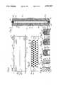
- FIG. 1 is a side elevational view showing a connector of the invention installed between a pair of circuit boards;
- FIG. 2 is a top plan view of the connector of FIG. 1;
- FIG. 3 is a sectional view on an enlarged scale, taken substantially along line III--III of FIG. 2;
- FIG. 4 is a sectional view corresponding to an upper portion of FIG. 3, but with a button removed to show the form of cavity surfaces;
- FIG. 5 is a sectional view similar to FIG. 4, but showing modification with a button attached to a slug by crimping;
- FIGS. 6 and 7 illustrate modifications in which buttons are bonded to a slug, through an adhesive or through a welding or soldering operation.
- Reference numeral 10 generally designates an electrical connector which is constructed in accordance with the principles of the invention and which is shown installed between two circuit boards 11 and 12 which are compressibly positioned by two bolts 13 and 14.
- the connector 10 functions to interconnect circuits on the boards 11 and 12 and also functions as a spacer between the boards 11 and 12.
- One or more additional connectors may be used in connecting and spacing two boards and/or in connecting and spacing three or more circuit boards in stacked relation.
- the vertical dimensions of the connectors may be selected in accordance with the vertical extent of components on the boards and connectors with different vertical dimensions may be used to connect three or more stacked boards. In each case the connectors of the invention operate to provide signal propagation paths between the boards which have short lengths and which are highly reliable.
- the connectors of the invention are also readily installed by simply sandwiching the connectors between boards and clamping the boards and connectors together.
- the connector 10 includes a block 16 which is of insulating material and which has upper and lower planar surfaces 17 and 18.
- Block 16 is preferably formed by upper and lower members 19 and 20 respectively having lower and upper surfaces 21 and 22 engaging in a plane which is midway between the surfaces 17 and 18 in the illustrated connector but which may be positioned at unequal distances from the surfaces 17 and 18.
- buttons 25 are mounted in cavities in the upper surface 17 of the block 16 for engagement with the conductive pads on the underside of the circuit board 11 and corresponding series of conductive buttons 26 are mounted in cavities in the lower surface 18 of the block 16 for engagement with the conductive pads on the upperside of the circuit board 18.
- Each of the buttons may typically be in the form of an elongated cylindrical contact element comprising a resiliently and randomly wadded thin gauge electrically conductive wire. Such buttons provide low impedance connections when proper contact pressures are maintained between such buttons and contact surfaces engaged thereby.
- buttons 25 and 26 To connect such buttons 25 and 26, a plurality of elongated slugs 28 of copper or other conductive material are provided within the block 16. The mounting of two of such buttons 25 and 26 and the connection thereof by one of such slugs 28 is shown in the sectional view of FIG. 3.
- the slug 28 is positioned in an opening in the block 16 which is defined by aligned openings 29 and 30 in the upper and lower members 19 and 20, the slug being so positioned that terminal upper and lower end surfaces thereof are respectively spaced at substantially equal distances below and above the upper and lower surfaces 17 and 18 of the block 16 to provide cavities which receive the buttons 25 and 26 and which are generally designated by reference numerals 31 and 32. Only the cavity 31 at the upper end of the illustrated slug 28 will be described in detail, the cavity at the lower end and other cavities of the connector being of substantially the same form.
- the cavity 31 in the upper member 19 has an "hour glass" shape and is defined by surface portions which include an intermediate neck portion 33, an inner flared portion 34 and an outer flared portion 35.
- the remainder of the opening 29 in the upper member 19 is defined by a right cylindrical surface portion 36 which extends downwardly from the lower end of the lower surface portion 34 of the cavity.
- the neck portion 33 has a very small axial dimension and applies a localized compressive pressure to the button 25 when installed to securely hold the button 25 in place while allowing free resilient axial compression of the button 25 to obtain reliable low resistance connections.
- the inner flared portion 34 provides an expansion region into which a lower portion of the button expands when the button is installed, to additionally insure the secured holding of the button in place while allowing free resilient axial compression thereof.
- the outer flared portion 35 facilitates installation of the button and avoids entrapment of any protruding fine wire portions of the button between facing surfaces of the connector and circuit board. It also facilitates the free axial compression of the button when installed and accommodates any slight transverse relative shifting movements of the connector and circuit board as may occur during or after assembly. It preferably is of very smooth form, facilitating installation of the buttons and avoiding sharp edges which might catch and cause entrapment of protruding wire portions of the buttons.
- the members 19 and 20 are moved together while positioning the slugs 28 to enter the openings of the members 19 and 20 at the surfaces 21 and 22 thereof, so that the slugs 28 do not pass through the cavity-defining surfaces.
- the slugs may preferably be installed with a press fit using fixtures to obtain accurate positioning thereof.
- Slugs 28 may preferably include collar portions 28A and 28B adjacent the terminal ends thereof, providing localized pressure engagement with the block members 19 and 20.
- the block members 19 and 20 may be secured together by any suitable means, such as use of an adhesive at the interface of surfaces 21 and 22.
- press-fit engagement of the slugs in the openings 29 and 30 may be utilized for effecting such securement of the members 19 and 20 to one another, with the slugs in place, to form the base connector assembly.
- the buttons 25 and 26 are installed in the cavities 31 and 32.
- the button 25 may be of generally right cylindrical shape with a diameter substantially less than that of the outer flared portion 35 and only slightly greater than that of the neck portion 33, sufficient to securely hold the button in place while allowing free axial compression thereof to obtain electrically efficient contact pressures.
- Such contact pressures are provided when the connector 10 is clamped in its operative position between circuit boards, as in FIG. 1 wherein the bolts 13 provide the clamping force, or between other components to be connected.
- conductive pad areas on the respective spaced components are axially pressed against the exposed distal end surfaces of the buttons 25 and 26 of a respective button-and-slug conductor path and thereby are effectively connected in electrically conductive contact with one another through the connector 10.
- FIG. 5 illustrates a modification in which a button 40 is inserted into a hollow end portion of a slug 42 which is positioned in an opening 43 of a block member 44.
- a terminal end 42A of the slug 42 is crimped inwardly into locking engagement with an inner end portion of the button to securely hold the button 40 while allowing free resilient axial compression of the button to obtain an electrically efficient contact pressure.
- the opening 43 has a uniform diameter which is greater than that of the button 40.
- the block in this case may be formed by the single member 44 with a button affixed through crimping to the opposite end of the slug 42.
- FIGS. 6 and 7 In place of the crimping arrangement of FIG. 5, arrangements as shown in FIGS. 6 and 7 may be used, in which a button is bonded to a slug.
- a button 46 is secured through a weld or solder bond, indicated by reference numeral 47, to the end of a slug 49 disposed in an opening 49 in a block member 50.
- a button 52 is secured through an adhesive 53 to the end of a slug 54 disposed in an opening 55 of a block member 56.
- the adhesive 54 may be in a small centrally located pocket in the surface of the slug, to permit electrical contact between the major portion of the button 52 and the terminal end surface of the plug 54 or the adhesive may be an electrically conductive adhesive.
- the surfaces of the slugs 28 may be engaged with or in close proximity to the walls of the openings 29 and 30, or there may be a substantial radial spacing between the surfaces of the slugs 28 and the walls of the openings 29 and 30 such as is provided when using the collars 28A and 28B as shown in FIG. 3.
- the relative radial dimensions of the slugs 28 and the walls of the openings 29 and 30 affect the impedance of the conductive paths through the slugs.
- predetermined dimensional values to control the impedance of the connections being effected.
- shielding may be placed around the connector 10, with or without the use of central ground planes for further providing shielding against EMI and RFI interference and for additional control of the impedance values, along the lines referred to in the aforementioned copending application Ser. No. 07/352,499 and in issued U.S. Pat. Nos. 4,710,133 and 4,806,110.
Abstract
Description
Claims (16)
Priority Applications (18)
| Application Number | Priority Date | Filing Date | Title |
|---|---|---|---|
| US07/375,588 US4992053A (en) | 1989-07-05 | 1989-07-05 | Electrical connectors |
| US07/406,142 US5013249A (en) | 1986-06-19 | 1989-09-12 | Electrical connectors |
| CA000614505A CA1313545C (en) | 1989-05-16 | 1989-09-29 | Electrical connectors |
| ES90917915T ES2067773T3 (en) | 1989-07-05 | 1990-06-26 | ELECTRICAL CONNECTORS. |
| EP90917915A EP0437606B1 (en) | 1989-07-05 | 1990-06-26 | Electrical connectors |
| PCT/US1990/003621 WO1991001051A1 (en) | 1989-07-05 | 1990-06-26 | Electrical connectors |
| JP2509639A JPH0732047B2 (en) | 1989-07-05 | 1990-06-26 | Electrical connector |
| DE69016189T DE69016189T2 (en) | 1989-07-05 | 1990-06-26 | ELECTRIC CONNECTORS. |
| JP2510380A JPH0793169B2 (en) | 1989-07-05 | 1990-06-28 | Electrical connector |
| ES94117641T ES2144027T3 (en) | 1989-07-05 | 1990-06-28 | ELECTRIC CONNECTOR. |
| DE69019830T DE69019830T2 (en) | 1989-07-05 | 1990-06-28 | ELECTRICAL CONNECTORS. |
| DE69033498T DE69033498T2 (en) | 1989-07-05 | 1990-06-28 | Electrical connector |
| EP94117641A EP0647088B1 (en) | 1989-07-05 | 1990-06-28 | Electrical connector |
| PCT/US1990/003640 WO1991001078A1 (en) | 1989-07-05 | 1990-06-28 | Electrical connectors |
| EP90911027A EP0509992B1 (en) | 1989-07-05 | 1990-06-28 | Electrical connectors |
| ES90911027T ES2073578T3 (en) | 1989-07-05 | 1990-06-28 | ELECTRICAL CONNECTORS. |
| US08/361,448 US5597313A (en) | 1986-06-19 | 1994-12-21 | Electrical connectors |
| US08/473,068 US6062870A (en) | 1989-05-16 | 1995-06-07 | Electrical interconnects |
Applications Claiming Priority (1)
| Application Number | Priority Date | Filing Date | Title |
|---|---|---|---|
| US07/375,588 US4992053A (en) | 1989-07-05 | 1989-07-05 | Electrical connectors |
Related Parent Applications (1)
| Application Number | Title | Priority Date | Filing Date |
|---|---|---|---|
| US07/352,499 Continuation US4988306A (en) | 1986-06-19 | 1989-05-16 | Low-loss electrical interconnects |
Related Child Applications (3)
| Application Number | Title | Priority Date | Filing Date |
|---|---|---|---|
| US07/352,499 Continuation-In-Part US4988306A (en) | 1986-06-19 | 1989-05-16 | Low-loss electrical interconnects |
| US64790791A Continuation | 1986-06-19 | 1991-01-30 | |
| US08/361,448 Continuation-In-Part US5597313A (en) | 1986-06-19 | 1994-12-21 | Electrical connectors |
Publications (1)
| Publication Number | Publication Date |
|---|---|
| US4992053A true US4992053A (en) | 1991-02-12 |
Family
ID=23481472
Family Applications (1)
| Application Number | Title | Priority Date | Filing Date |
|---|---|---|---|
| US07/375,588 Expired - Lifetime US4992053A (en) | 1986-06-19 | 1989-07-05 | Electrical connectors |
Country Status (6)
| Country | Link |
|---|---|
| US (1) | US4992053A (en) |
| EP (1) | EP0437606B1 (en) |
| JP (1) | JPH0732047B2 (en) |
| DE (1) | DE69016189T2 (en) |
| ES (1) | ES2067773T3 (en) |
| WO (1) | WO1991001051A1 (en) |
Cited By (19)
| Publication number | Priority date | Publication date | Assignee | Title |
|---|---|---|---|---|
| WO1992014280A1 (en) * | 1991-01-30 | 1992-08-20 | Labinal Components And Systems, Inc. | Electrical connectors |
| US5169320A (en) * | 1991-09-27 | 1992-12-08 | Hercules Defense Electronics Systems, Inc. | Shielded and wireless connector for electronics |
| US5356298A (en) * | 1993-04-01 | 1994-10-18 | Trw Inc. | Wideband solderless right-angle RF interconnect |
| US5382169A (en) * | 1994-01-14 | 1995-01-17 | Labinal Components And Systems, Inc. | Electrical connectors |
| US5597313A (en) * | 1986-06-19 | 1997-01-28 | Labinal Components And Systems, Inc. | Electrical connectors |
| US5618205A (en) * | 1993-04-01 | 1997-04-08 | Trw Inc. | Wideband solderless right-angle RF interconnect |
| US5672062A (en) * | 1991-01-30 | 1997-09-30 | Labinal Components And Systems, Inc. | Electrical connectors |
| US5704794A (en) * | 1986-12-29 | 1998-01-06 | Labinal Components And Systems, Inc. | Electrical connectors |
| US5761036A (en) * | 1989-06-09 | 1998-06-02 | Labinal Components And Systems, Inc. | Socket assembly for electrical component |
| US5800184A (en) * | 1994-03-08 | 1998-09-01 | International Business Machines Corporation | High density electrical interconnect apparatus and method |
| US6062870A (en) * | 1989-05-16 | 2000-05-16 | Labinal Components And Systems, Inc. | Electrical interconnects |
| WO2000048263A1 (en) * | 1999-02-12 | 2000-08-17 | Raytheon Company | Control impedance rf pin for extending compressible button interconnect contact distance |
| US6375473B1 (en) | 2000-05-05 | 2002-04-23 | Kelsey-Hayes Company | Electrical interconnection for an electro-hydraulic brake system using wire form buttons |
| US20020184759A1 (en) * | 1998-08-17 | 2002-12-12 | Siemens Aktiengesellschaft | Process for producing a contact-making device |
| US6537082B2 (en) | 1997-10-23 | 2003-03-25 | Cinch Connectors, Inc. | Electrical connector |
| US20040266224A1 (en) * | 2003-06-27 | 2004-12-30 | Watson Troy M. | Active configurable and stackable interface connector |
| US7168958B1 (en) * | 2005-08-25 | 2007-01-30 | International Business Machines Corporation | Wadded-wire LGA contact with parallel solid conductor |
| US20070111600A1 (en) * | 2005-11-16 | 2007-05-17 | Takashi Tokunaga | Connector, mating connector and board-to-board connector assembly |
| WO2012071333A1 (en) * | 2010-11-23 | 2012-05-31 | Cinch Connectors, Inc. | Electrical connector |
Families Citing this family (2)
| Publication number | Priority date | Publication date | Assignee | Title |
|---|---|---|---|---|
| DE9410341U1 (en) * | 1994-06-27 | 1994-11-24 | Siemens Ag | Backplane PCB arrangement for plug connections |
| US7074047B2 (en) * | 2003-11-05 | 2006-07-11 | Tensolite Company | Zero insertion force high frequency connector |
Citations (14)
| Publication number | Priority date | Publication date | Assignee | Title |
|---|---|---|---|---|
| US2853656A (en) * | 1953-08-07 | 1958-09-23 | Burroughs Corp | Printed circuit panel assembly |
| US3077511A (en) * | 1960-03-11 | 1963-02-12 | Int Resistance Co | Printed circuit unit |
| US3200297A (en) * | 1962-05-18 | 1965-08-10 | Randac Systems Inc | Control unit having removable and interchangeable programming inserts |
| US3616532A (en) * | 1970-02-02 | 1971-11-02 | Sperry Rand Corp | Multilayer printed circuit electrical interconnection device |
| US3795047A (en) * | 1972-06-15 | 1974-03-05 | Ibm | Electrical interconnect structuring for laminate assemblies and fabricating methods therefor |
| US3795037A (en) * | 1970-05-05 | 1974-03-05 | Int Computers Ltd | Electrical connector devices |
| US3862790A (en) * | 1971-07-22 | 1975-01-28 | Plessey Handel Investment Ag | Electrical interconnectors and connector assemblies |
| US3904934A (en) * | 1973-03-26 | 1975-09-09 | Massachusetts Inst Technology | Interconnection of planar electronic structures |
| US4029375A (en) * | 1976-06-14 | 1977-06-14 | Electronic Engineering Company Of California | Miniature electrical connector |
| US4257661A (en) * | 1977-10-28 | 1981-03-24 | Technical Wire Products, Inc. | Retainer for elastomeric electrical connector |
| US4574331A (en) * | 1983-05-31 | 1986-03-04 | Trw Inc. | Multi-element circuit construction |
| US4581679A (en) * | 1983-05-31 | 1986-04-08 | Trw Inc. | Multi-element circuit construction |
| US4636018A (en) * | 1985-06-05 | 1987-01-13 | Amp Incorporated | Elastomeric electrical connector |
| US4733172A (en) * | 1986-03-08 | 1988-03-22 | Trw Inc. | Apparatus for testing I.C. chip |
Family Cites Families (2)
| Publication number | Priority date | Publication date | Assignee | Title |
|---|---|---|---|---|
| US4593961A (en) * | 1984-12-20 | 1986-06-10 | Amp Incorporated | Electrical compression connector |
| US4843313A (en) * | 1984-12-26 | 1989-06-27 | Hughes Aircraft Company | Integrated circuit package carrier and test device |
-
1989
- 1989-07-05 US US07/375,588 patent/US4992053A/en not_active Expired - Lifetime
-
1990
- 1990-06-26 ES ES90917915T patent/ES2067773T3/en not_active Expired - Lifetime
- 1990-06-26 EP EP90917915A patent/EP0437606B1/en not_active Expired - Lifetime
- 1990-06-26 DE DE69016189T patent/DE69016189T2/en not_active Expired - Fee Related
- 1990-06-26 JP JP2509639A patent/JPH0732047B2/en not_active Expired - Lifetime
- 1990-06-26 WO PCT/US1990/003621 patent/WO1991001051A1/en active IP Right Grant
Patent Citations (14)
| Publication number | Priority date | Publication date | Assignee | Title |
|---|---|---|---|---|
| US2853656A (en) * | 1953-08-07 | 1958-09-23 | Burroughs Corp | Printed circuit panel assembly |
| US3077511A (en) * | 1960-03-11 | 1963-02-12 | Int Resistance Co | Printed circuit unit |
| US3200297A (en) * | 1962-05-18 | 1965-08-10 | Randac Systems Inc | Control unit having removable and interchangeable programming inserts |
| US3616532A (en) * | 1970-02-02 | 1971-11-02 | Sperry Rand Corp | Multilayer printed circuit electrical interconnection device |
| US3795037A (en) * | 1970-05-05 | 1974-03-05 | Int Computers Ltd | Electrical connector devices |
| US3862790A (en) * | 1971-07-22 | 1975-01-28 | Plessey Handel Investment Ag | Electrical interconnectors and connector assemblies |
| US3795047A (en) * | 1972-06-15 | 1974-03-05 | Ibm | Electrical interconnect structuring for laminate assemblies and fabricating methods therefor |
| US3904934A (en) * | 1973-03-26 | 1975-09-09 | Massachusetts Inst Technology | Interconnection of planar electronic structures |
| US4029375A (en) * | 1976-06-14 | 1977-06-14 | Electronic Engineering Company Of California | Miniature electrical connector |
| US4257661A (en) * | 1977-10-28 | 1981-03-24 | Technical Wire Products, Inc. | Retainer for elastomeric electrical connector |
| US4574331A (en) * | 1983-05-31 | 1986-03-04 | Trw Inc. | Multi-element circuit construction |
| US4581679A (en) * | 1983-05-31 | 1986-04-08 | Trw Inc. | Multi-element circuit construction |
| US4636018A (en) * | 1985-06-05 | 1987-01-13 | Amp Incorporated | Elastomeric electrical connector |
| US4733172A (en) * | 1986-03-08 | 1988-03-22 | Trw Inc. | Apparatus for testing I.C. chip |
Non-Patent Citations (1)
| Title |
|---|
| IBM Technical Disclosure Bulletin, vol. 22, No. 1, 1979; pp. 158, 159. * |
Cited By (28)
| Publication number | Priority date | Publication date | Assignee | Title |
|---|---|---|---|---|
| US5597313A (en) * | 1986-06-19 | 1997-01-28 | Labinal Components And Systems, Inc. | Electrical connectors |
| US5704794A (en) * | 1986-12-29 | 1998-01-06 | Labinal Components And Systems, Inc. | Electrical connectors |
| US6062870A (en) * | 1989-05-16 | 2000-05-16 | Labinal Components And Systems, Inc. | Electrical interconnects |
| US5761036A (en) * | 1989-06-09 | 1998-06-02 | Labinal Components And Systems, Inc. | Socket assembly for electrical component |
| US5704795A (en) * | 1991-01-30 | 1998-01-06 | Labinal Components And Systems, Inc. | Electrical connectors |
| WO1992014281A1 (en) * | 1991-01-30 | 1992-08-20 | Labinal Components And Systems, Inc. | Electrical connectors |
| US5788512A (en) * | 1991-01-30 | 1998-08-04 | Labinal Components And Systems, Inc. | Electrical connectors |
| WO1992014280A1 (en) * | 1991-01-30 | 1992-08-20 | Labinal Components And Systems, Inc. | Electrical connectors |
| US5672062A (en) * | 1991-01-30 | 1997-09-30 | Labinal Components And Systems, Inc. | Electrical connectors |
| US5169320A (en) * | 1991-09-27 | 1992-12-08 | Hercules Defense Electronics Systems, Inc. | Shielded and wireless connector for electronics |
| US5618205A (en) * | 1993-04-01 | 1997-04-08 | Trw Inc. | Wideband solderless right-angle RF interconnect |
| US5356298A (en) * | 1993-04-01 | 1994-10-18 | Trw Inc. | Wideband solderless right-angle RF interconnect |
| US5382169A (en) * | 1994-01-14 | 1995-01-17 | Labinal Components And Systems, Inc. | Electrical connectors |
| US5569039A (en) * | 1994-01-14 | 1996-10-29 | Labinal Components And Systems, Inc. | Electrical connectors |
| US5800184A (en) * | 1994-03-08 | 1998-09-01 | International Business Machines Corporation | High density electrical interconnect apparatus and method |
| US6537082B2 (en) | 1997-10-23 | 2003-03-25 | Cinch Connectors, Inc. | Electrical connector |
| US6948242B2 (en) | 1998-08-17 | 2005-09-27 | Infineon Technologies Ag | Process for producing a contact-making device |
| US20020184759A1 (en) * | 1998-08-17 | 2002-12-12 | Siemens Aktiengesellschaft | Process for producing a contact-making device |
| WO2000048263A1 (en) * | 1999-02-12 | 2000-08-17 | Raytheon Company | Control impedance rf pin for extending compressible button interconnect contact distance |
| US6375473B1 (en) | 2000-05-05 | 2002-04-23 | Kelsey-Hayes Company | Electrical interconnection for an electro-hydraulic brake system using wire form buttons |
| US20040266224A1 (en) * | 2003-06-27 | 2004-12-30 | Watson Troy M. | Active configurable and stackable interface connector |
| WO2005006496A2 (en) * | 2003-06-27 | 2005-01-20 | Watson Troy M | Active configurable and stackable interface connector |
| WO2005006496A3 (en) * | 2003-06-27 | 2005-06-02 | Troy M Watson | Active configurable and stackable interface connector |
| US6942494B2 (en) * | 2003-06-27 | 2005-09-13 | Troy M. Watson | Active configurable and stackable interface connector |
| US7168958B1 (en) * | 2005-08-25 | 2007-01-30 | International Business Machines Corporation | Wadded-wire LGA contact with parallel solid conductor |
| US20070111600A1 (en) * | 2005-11-16 | 2007-05-17 | Takashi Tokunaga | Connector, mating connector and board-to-board connector assembly |
| US7503773B2 (en) | 2005-11-16 | 2009-03-17 | Japan Aviation Electronics Industry, Limited | Connector, mating connector and board-to-board connector assembly |
| WO2012071333A1 (en) * | 2010-11-23 | 2012-05-31 | Cinch Connectors, Inc. | Electrical connector |
Also Published As
| Publication number | Publication date |
|---|---|
| JPH04500433A (en) | 1992-01-23 |
| EP0437606B1 (en) | 1995-01-18 |
| DE69016189T2 (en) | 1995-09-14 |
| EP0437606A4 (en) | 1992-11-04 |
| WO1991001051A1 (en) | 1991-01-24 |
| JPH0732047B2 (en) | 1995-04-10 |
| EP0437606A1 (en) | 1991-07-24 |
| DE69016189D1 (en) | 1995-03-02 |
| ES2067773T3 (en) | 1995-04-01 |
Similar Documents
| Publication | Publication Date | Title |
|---|---|---|
| US4992053A (en) | Electrical connectors | |
| US5427535A (en) | Resilient electrically conductive terminal assemblies | |
| US4487464A (en) | Electrical socket connector construction | |
| US4682829A (en) | Surface mount socket for dual in-line package | |
| EP0663704B1 (en) | Electrical connectors | |
| US4422128A (en) | Push-on terminal clip and assembly | |
| JPH08124637A (en) | Surface-mounting electric connector | |
| KR940004894A (en) | Coaxial Connector for 2 Board Connection | |
| US4824384A (en) | Electrical cable connector and method of use | |
| US20080018353A1 (en) | Methods and apparatus for releasably mounting a semiconductor device to a printed circuit board | |
| JPH08512428A (en) | Improvements regarding coaxial connectors | |
| US4045114A (en) | Method of manufacturing an electrical connector | |
| JP3703521B2 (en) | Pin socket connector for board mounting | |
| CA2307922C (en) | Surface-mount electrical connection device | |
| EP1120870A2 (en) | Termination adapter for PCB | |
| US3900239A (en) | Electrical socket adaptor | |
| EP0461391B1 (en) | Electrical test probe having integral strain relief and ground connection | |
| JPS6229084A (en) | Contactor and manufacture thereof | |
| JP4049230B2 (en) | Microwave device | |
| US4638406A (en) | Discrete component mounting assembly | |
| US3850498A (en) | Filter assembly for printed circuit board connectors | |
| CA1313545C (en) | Electrical connectors | |
| US3506879A (en) | Circuit board terminals with laced conductor means | |
| US6095857A (en) | Electrical component for surface-mounting on a circuit board | |
| FI89842C (en) | FJAEDRANDE KONTAKTDON FOER RADIOFREKVENTA SIGNALER |
Legal Events
| Date | Code | Title | Description |
|---|---|---|---|
| AS | Assignment |
Owner name: LABINAL COMPONENTS AND SYSTEMS, INC., 1501 MORSE A Free format text: ASSIGNMENT OF ASSIGNORS INTEREST.;ASSIGNOR:LINDEMAN, RICHARD J.;REEL/FRAME:005099/0368 Effective date: 19890705 |
|
| STCF | Information on status: patent grant |
Free format text: PATENTED CASE |
|
| FEPP | Fee payment procedure |
Free format text: PAYOR NUMBER ASSIGNED (ORIGINAL EVENT CODE: ASPN); ENTITY STATUS OF PATENT OWNER: LARGE ENTITY |
|
| FPAY | Fee payment |
Year of fee payment: 4 |
|
| FPAY | Fee payment |
Year of fee payment: 8 |
|
| AS | Assignment |
Owner name: CINCH CONNECTORS, INC., ILLINOIS Free format text: ASSIGNMENT OF ASSIGNORS INTEREST;ASSIGNOR:LABINAL COMPONENTS AND SYSTEMS, INC.;REEL/FRAME:011511/0595 Effective date: 20001212 |
|
| FPAY | Fee payment |
Year of fee payment: 12 |