BACKGROUND OF THE INVENTION
1. Field of the Invention
This invention pertains to the field of digital signal processing and, in particular, to the matrix multiplication of a plurality of digital signals by a coefficient matrix of the type used in color video signal processing.
2. Background Art
Correction matrices are useful in a variety of color video applications. For instance, a conversion matrix is used to convert red, green, and blue video signals into Y (luminance) and I, Q (chrominance) signals. A color correction matrix is used to correct the spectral sensitivities of a video camera for the chromaticities of the phosphor set of the particular display in use. Another use is with film-to-video conversion, a process in which a color correction matrix operates on the film scanning signals to correct the film colorimetry for video display.
It is desirable for reasons of space and efficiency to implement the matrix in one, or a few, integrated circuits. A conventional approach is to use an array of multipliers, say nine multipliers, to implement a 3×3 matrix. This uses a prohibitive amount of circuit area (on an integrated circuit). The multipliers can be replaced with ROM (read only memory) look-up tables. This still takes too much area. Another approach approximates the matrix coefficients by simple shifting operations, which can be implemented digitally by "hardwired" right (or left) shift connections between registers that provide a "binary" matrix coefficient series, such as 1/32, 1/16, 1/8, 1/4, 1/2, 1, 2, etc. Such poor coefficient accuracy can be improved by summing selected coefficients, but this requires many adders and many shifts. Once again, too much area is required.
In U.S. Pat. No. 4,507,676, a compromise solution is disclosed in which each coefficient is broken into two parts: a binary part and a remainder. The binary part is implemented by a "hardwired" right shift and the remainder is implemented by a ROM look-up table. While such an approach provides additional accuracy, it would be desirable to eliminate the ROM look-up tables altogether. Moreover, in view of the disparate applications for video matrices, it would be greatly preferred to have a universal matrix chip that could be used for a variety of applications with a minimum of redesign.
SUMMARY OF THE INVENTION
The invention departs from the prior art by mask-programming both the shifts and an arithmetic function in a simple, area-conserving configuration that lends itself to cascading, both for increased accuracy and ease of matrix implementation. The basis of the approach is the realization that by either adding or subtracting two "hardwired" shifted inputs, it is possible to obtain most of the desired matrix coefficients with a very small amount of circuitry. For instance, two input digital signals are separately multiplied or divided by programmable powers of two according to programmable bit shifts, yielding first and second intermediate signals. The intermediate signals are then arithmetrically combined according to a programmable arithmetic function, say addition or subtraction, to provide a product signal. By selecting the arithmetic function and defining the bit lengths of the shifts, the multiplier coefficient, or a component thereof, is established.
This programmable circuit becomes a "building block" in which a plurality of like circuits are cascaded such that the output of one becomes the input to another for all but one such circuit that provides the matrix output signal. In such manner, the accuracy of each coefficient may be improved and at least one channel (row) of a matrix may be implemented. A multi-row matrix is obtained by driving several cascaded chains in parallel across a plurality of signal channels.
BRIEF DESCRIPTION OF THE DRAWINGS
The invention will be described in relation to the drawings, in which
FIG. 1 is a block diagram of a multi-channel video matrix circuit for performing a color correction;
FIG. 2 is a detailed diagram of the programmable matrix in the red channel shown in FIG. 1; and
FIG. 3 illustrates one of the programmable circuit blocks shown in FIG. 2.
DETAILED DESCRIPTION OF A PREFERRED EMBODIMENT
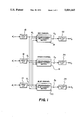
Referring first to FIG. 1, a typical video matrix application is shown in which the matrix coefficients correct the spectral sensitivities of a video camera for the chromaticities of a particular phosphor display. The matrix is implemented in separate red, green and blue channels, as shown. A set of input signals R'i, G'i, and B'i from a video camera (not shown) are applied to separate ROM (read only memory) look-up tables 10, 12 and 14, which convert the input signals from the input mathematical space to a linear mathematical space. Since the preferred embodiment is used with logarithmic input signals, the tables 10, 12, and 14 convert the respective input log signals to a set of linear signals Ri, Gi, and Bi. A color correction matrix is implemented row-by-row across the separate channels by a programmable red channel matrix 16, a programmable green channel matrix 18, and a programmable blue channel matrix 20. The linear signals Ri, Gi, and Bi are applied to each of the matrixes 16, 18, and 20 for multiplication by an array of coefficients aij. The color correction matrix operation is shown in equation (1), ##EQU1## where Ro, Go, and Bo are the signals output from the respective matrix circuits 16, 18, and 20.
The coefficients aij depend on the color-mixture functions of the phosphors used in the television display and the spectral sensitivities of the three color signals from the video camera, which includes the optics and the sensor. The coefficients can be positive or negative. In general, negative off-diagonal coefficients increase the color saturation of the image. Since it is ordinarily desirable to keep the sum of the coefficients in a given row equal to one, the diagonal coefficient is made greater than one to offset the negative off-diagonal coefficients. In this embodiment, the coefficients are selected as shown in equation (2) for improved color rendition and color saturation, ##EQU2## where the coefficients aij are selected for color correction in relation to a SMPTE "C" phosphor display, that is, a phosphor characteristic established by the Society of Motion Picture and Television Engineers.
Each matrix 16, 18, and 20 implements a respective row of the matrix multiplication. For this reason, all signals Ri, Gi, and Bi are applied to each matrix 16, 18, and 20. The matrix operation uses constrained shift and add/subtract operations together with pipelining and parallelism as shown in FIG. 2 (for the red channel). This architecture avoids the use of multipliers. The coefficients are metal mask programmable between +/-1/32 and +/-2 at discrete (not necessarily equal) increments. The programmability allows the matrix circuit to be used with different image sensor spectral sensitivities or with different types of displays by changing a single mask. The matrix output signals Ro, Go, and Bo are then gamma-corrected in respective linear to gamma ROM look-up tables 22, 24, and 26, which provide suitable curve shape transformations to adjust the non-linear contrast relationship between the signal voltages at the input and the light values at the output of the system. The gamma-corrected output signals R'o, G'o, and B'o are suitably connected to a video display (not shown).
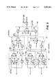
In FIG. 1, the full matrix is shown implemented in three 1×3 matrix channels. Referring now to FIG. 2, the 1×3 red matrix channel is shown in greater detail. The red matrix channel (as well as the green and blue matrix channels) includes metal mask programmable shift/add/subtract digital blocks, each basically identical and identified by the reference character 30. Each digital block 30 includes two registers 32 with mask programmable input shifts, each register basically identical except for the programmed shifts, and a mask programmable arithmetic unit 34. The registers 32 are mask programmed to provide the divisions as shown, i.e., a shift of one bit for 1/2, two bits for 1/4, three bits for 1/8, etc. The arithmetic unit 34 includes data inputs a and b, the input b capable of being negated by mask programming of a control input a/s thereof.
As shown in FIG. 2, the digital blocks 30 are cascaded whereby the output of one becomes the input to another, excepting for the last digital block 30, which provides the matrix output signal Ro (i.e., R o 13/8R i 1/4Gi 3/8Bi). It is further shown that the diagonal coefficient a11 (equation (1)) is calculated by the cascaded arrangement 36 of two blocks 30a and 30b. According to the arrangement 36, the red input signal Ri is directed to both inputs of the upstream digital block 30a and one input of the following downstream block 30b. This is useful in providing coefficients of greater than one. The green and blue channel matrices are implemented with an architecture identical to that shown in FIG. 2, except that the cascaded arrangement 36 is provided for either the green or blue input signal Gi or Bi, respectively, instead of for the red input signal Ri. The shifts and the arithmetic functions are of course altered as necessary to obtain the desired coefficients.
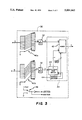
FIG. 3 shows one of the digital blocks 30 in greater detail. The input bit resolution m and the output bit resolution n depend on whether the block 30 is an input, middle, or output block in the matrix channel, as shown in FIG. 2. For instance, the blocks 30 connected to the inputs Ri, Gi and Bi have m=10 input bits and n=12 output bits. FIG. 3 shows the internal construction of the block 30 and how the matrix coefficient "7/32" is mask programmed. The registers 32 include mask programmable input arrays identified as "hardwired" inputs 40a and 40b. Simple metal mask level alterations provide multiplication or division by a programmable power of two, that is, multiplication by 2n for a number (n) of left shifts or division by 1/2n for a number(n) of right shifts.
The arithmetic unit 34 includes an adder 42 and an array 44 of n exclusive NOR gates, which together form a 2's complement adder. The adder 42 has one input a of n bits connected to the output of the "a" register 32 and a second input b of n bits connected to the array 44 of NOR gates, which are in turn connected to the output of the "b" register 32. The array 44 of NOR gates and the adder 42 receive a negating input ADD/SUB ("a/s" in FIG. 2) from a sign generator 46. For mask programming of "7/32", the input 40a is "hardwired" by a simple metal mask level change to shift right two places to implement "x 1/4" while the input 40b is "hardwired" to shift right five places to implement "x 1/32". The most significant bits (MSB) thus bypassed in the shift are set to zero by "hardwiring" a digital "zero". The sign generator 46 is "hardwired" to digital "1" (Vcc) to implement a negation (providing "x-1/32"). This sets the ADD/SUB line=1, so that the array 44 of exclusive NOR gates inverts the signal to the input b and the adder carry input of the adder 42 is set to 1, thus providing the proper 2's complement subtraction. In the opposite case, when the sign generator 46 is "hardwired" to digital "O", the ADD/SUB line=0 and the adder 42 effects an addition (providing "9/32"). Alternately, an array of exclusive OR gates could be used in place of the array 44 of exclusive NOR gates if the ADD/SUB control lines are reversed, as is well known to those skilled in the art of digital circuit design.
FIGS. 1-3 show how the programmable digital circuit is mask programmed for color correction in a video camera application. The programmable digital circuit could also be mask programmed as a conversion matrix to convert red, green and blue video signals into Y (luminance) and I, Q (chrominance) signals. The input look-up tables 10, 12, and 14 would be mask programmed for gamma correction and the output look-up tables 22, 24, and 26 would be mask programmed for a unity, or "straight line", curve transformation. The selection of suitable matrix coefficients for such a conversion is well within the ordinary skill of this art. Another application would be in a film to video conversion, such as for a telecine machine. In this case log masking is required because the red, green, and blue video signals are being mapped through the approximately logarithmic characteristic curve of a film system to determine the red, green and blue recorded from the original scene, that is, the actual dye amounts formed in the image. The input look-up tables 10, 12, and 14 would be mask programmed for a "straight line" curve transformation, thus keeping the input signals Ri, Gi, and Bi in log space. The logarithmically quantized signals are next matrixed with a 3×3 color correction matrix which has been mask programmed in order to properly correct the film colorimetry for video display. A suitable array of coefficients is well known in the art and thus not set forth here. The output look-up tables 22, 24, and 26 would then be mask programmed to convert the log signals into gamma corrected signals.
Another application is in the conversion of the input signal from the color and tone scale of the instantaneously available video image to a color and tone scale matching a desired non-video output medium. For instance, in an apparatus where an image is simultaneously captured on film and with a video camera, the color and tone scale of the video image should match the appearance of the photographic print which will eventually be made. The linear signals Ri, Gi, and Bi are multiplied by a 3×3 color correction matrix which has been mask programmed in order to best correct the spectral sensitivities of the camera so that the display colors are similar to the color reproduction of prints from film. A suitable set of coefficients can be selected or estimated from a knowledge of the required transformation, such knowledge being within the conventional teaching in this art. The output ROM look-up tables 22, 24, and 26 are mask programmed to convert from linear space to a "gamma corrected" space matched to the curve shape of the output medium (e.g., a photographic paper), so that the video display tone scale will match the print tone scale.
The invention has been described in detail with particular reference to a presently preferred embodiment, but it will be understood that variations and modifications can be effected within the spirit and scope of the invention.