US5010024A - Passivation for integrated circuit structures - Google Patents
Passivation for integrated circuit structures Download PDFInfo
- Publication number
- US5010024A US5010024A US07/353,169 US35316989A US5010024A US 5010024 A US5010024 A US 5010024A US 35316989 A US35316989 A US 35316989A US 5010024 A US5010024 A US 5010024A
- Authority
- US
- United States
- Prior art keywords
- layer
- metal layer
- silicon nitride
- compressive stress
- voids
- Prior art date
- Legal status (The legal status is an assumption and is not a legal conclusion. Google has not performed a legal analysis and makes no representation as to the accuracy of the status listed.)
- Expired - Lifetime
Links
- 238000002161 passivation Methods 0.000 title description 31
- 229910052751 metal Inorganic materials 0.000 claims abstract description 167
- 239000002184 metal Substances 0.000 claims abstract description 167
- 229910052581 Si3N4 Inorganic materials 0.000 claims abstract description 155
- HQVNEWCFYHHQES-UHFFFAOYSA-N silicon nitride Chemical compound N12[Si]34N5[Si]62N3[Si]51N64 HQVNEWCFYHHQES-UHFFFAOYSA-N 0.000 claims abstract description 154
- 150000002500 ions Chemical class 0.000 claims abstract description 82
- 230000015572 biosynthetic process Effects 0.000 claims abstract description 62
- XUIMIQQOPSSXEZ-UHFFFAOYSA-N Silicon Chemical compound [Si] XUIMIQQOPSSXEZ-UHFFFAOYSA-N 0.000 claims abstract description 49
- 229910052710 silicon Inorganic materials 0.000 claims abstract description 46
- 239000010703 silicon Substances 0.000 claims abstract description 46
- 230000035515 penetration Effects 0.000 claims abstract description 40
- 238000000034 method Methods 0.000 claims abstract description 34
- 239000000356 contaminant Substances 0.000 claims abstract description 27
- 230000008859 change Effects 0.000 claims abstract description 15
- VYPSYNLAJGMNEJ-UHFFFAOYSA-N Silicium dioxide Chemical compound O=[Si]=O VYPSYNLAJGMNEJ-UHFFFAOYSA-N 0.000 claims abstract description 14
- 230000002401 inhibitory effect Effects 0.000 claims abstract 3
- 235000012239 silicon dioxide Nutrition 0.000 claims abstract 3
- 239000000377 silicon dioxide Substances 0.000 claims abstract 3
- XKRFYHLGVUSROY-UHFFFAOYSA-N Argon Chemical compound [Ar] XKRFYHLGVUSROY-UHFFFAOYSA-N 0.000 claims description 14
- 238000000151 deposition Methods 0.000 claims description 13
- BLRPTPMANUNPDV-UHFFFAOYSA-N Silane Chemical compound [SiH4] BLRPTPMANUNPDV-UHFFFAOYSA-N 0.000 claims description 11
- 238000004519 manufacturing process Methods 0.000 claims description 11
- 229910000077 silane Inorganic materials 0.000 claims description 10
- 238000002513 implantation Methods 0.000 claims description 9
- 238000005468 ion implantation Methods 0.000 claims description 9
- QGZKDVFQNNGYKY-UHFFFAOYSA-N Ammonia Chemical compound N QGZKDVFQNNGYKY-UHFFFAOYSA-N 0.000 claims description 8
- 229910052786 argon Inorganic materials 0.000 claims description 8
- 229910052814 silicon oxide Inorganic materials 0.000 claims description 8
- 239000000203 mixture Substances 0.000 claims description 7
- 230000015654 memory Effects 0.000 claims description 5
- ZOXJGFHDIHLPTG-UHFFFAOYSA-N Boron Chemical compound [B] ZOXJGFHDIHLPTG-UHFFFAOYSA-N 0.000 claims description 4
- 229910052785 arsenic Inorganic materials 0.000 claims description 4
- RQNWIZPPADIBDY-UHFFFAOYSA-N arsenic atom Chemical compound [As] RQNWIZPPADIBDY-UHFFFAOYSA-N 0.000 claims description 4
- 229910052796 boron Inorganic materials 0.000 claims description 4
- 229910052743 krypton Inorganic materials 0.000 claims description 4
- DNNSSWSSYDEUBZ-UHFFFAOYSA-N krypton atom Chemical compound [Kr] DNNSSWSSYDEUBZ-UHFFFAOYSA-N 0.000 claims description 4
- 229910052754 neon Inorganic materials 0.000 claims description 4
- GKAOGPIIYCISHV-UHFFFAOYSA-N neon atom Chemical compound [Ne] GKAOGPIIYCISHV-UHFFFAOYSA-N 0.000 claims description 4
- 229910021529 ammonia Inorganic materials 0.000 claims description 3
- -1 argon ions Chemical class 0.000 claims description 3
- IJGRMHOSHXDMSA-UHFFFAOYSA-N Atomic nitrogen Chemical compound N#N IJGRMHOSHXDMSA-UHFFFAOYSA-N 0.000 claims 14
- 229910052757 nitrogen Inorganic materials 0.000 claims 7
- 238000005229 chemical vapour deposition Methods 0.000 claims 2
- 239000007943 implant Substances 0.000 claims 2
- 239000010410 layer Substances 0.000 description 170
- 229910052782 aluminium Inorganic materials 0.000 description 13
- XAGFODPZIPBFFR-UHFFFAOYSA-N aluminium Chemical compound [Al] XAGFODPZIPBFFR-UHFFFAOYSA-N 0.000 description 13
- 239000000463 material Substances 0.000 description 11
- 238000011109 contamination Methods 0.000 description 9
- 230000008021 deposition Effects 0.000 description 8
- 238000011282 treatment Methods 0.000 description 8
- 238000006243 chemical reaction Methods 0.000 description 7
- 239000011800 void material Substances 0.000 description 7
- 230000002939 deleterious effect Effects 0.000 description 6
- 230000000694 effects Effects 0.000 description 6
- 238000005538 encapsulation Methods 0.000 description 6
- 238000005336 cracking Methods 0.000 description 5
- 239000008393 encapsulating agent Substances 0.000 description 5
- 238000007667 floating Methods 0.000 description 5
- 230000005540 biological transmission Effects 0.000 description 4
- 238000010276 construction Methods 0.000 description 4
- 230000008569 process Effects 0.000 description 4
- 230000008030 elimination Effects 0.000 description 3
- 238000003379 elimination reaction Methods 0.000 description 3
- 238000005516 engineering process Methods 0.000 description 3
- 238000009413 insulation Methods 0.000 description 3
- 230000005012 migration Effects 0.000 description 3
- 238000013508 migration Methods 0.000 description 3
- 230000005855 radiation Effects 0.000 description 3
- 239000000956 alloy Substances 0.000 description 2
- 229910045601 alloy Inorganic materials 0.000 description 2
- 229910001423 beryllium ion Inorganic materials 0.000 description 2
- 230000003247 decreasing effect Effects 0.000 description 2
- 239000007789 gas Substances 0.000 description 2
- 150000002739 metals Chemical class 0.000 description 2
- 239000012299 nitrogen atmosphere Substances 0.000 description 2
- 238000012545 processing Methods 0.000 description 2
- 239000000126 substance Substances 0.000 description 2
- 238000001771 vacuum deposition Methods 0.000 description 2
- 229910007277 Si3 N4 Inorganic materials 0.000 description 1
- 238000010521 absorption reaction Methods 0.000 description 1
- 238000005275 alloying Methods 0.000 description 1
- QVGXLLKOCUKJST-UHFFFAOYSA-N atomic oxygen Chemical compound [O] QVGXLLKOCUKJST-UHFFFAOYSA-N 0.000 description 1
- 238000006664 bond formation reaction Methods 0.000 description 1
- 239000002131 composite material Substances 0.000 description 1
- 238000005260 corrosion Methods 0.000 description 1
- 230000007797 corrosion Effects 0.000 description 1
- 239000013078 crystal Substances 0.000 description 1
- 239000003989 dielectric material Substances 0.000 description 1
- 239000002355 dual-layer Substances 0.000 description 1
- 230000005670 electromagnetic radiation Effects 0.000 description 1
- XUFQPHANEAPEMJ-UHFFFAOYSA-N famotidine Chemical compound NC(N)=NC1=NC(CSCCC(N)=NS(N)(=O)=O)=CS1 XUFQPHANEAPEMJ-UHFFFAOYSA-N 0.000 description 1
- 239000012467 final product Substances 0.000 description 1
- 230000006870 function Effects 0.000 description 1
- 239000012774 insulation material Substances 0.000 description 1
- 230000007246 mechanism Effects 0.000 description 1
- 230000004048 modification Effects 0.000 description 1
- 238000012986 modification Methods 0.000 description 1
- 229910000069 nitrogen hydride Inorganic materials 0.000 description 1
- 230000003287 optical effect Effects 0.000 description 1
- 239000001301 oxygen Substances 0.000 description 1
- 229910052760 oxygen Inorganic materials 0.000 description 1
- 239000000047 product Substances 0.000 description 1
- 239000000376 reactant Substances 0.000 description 1
- 230000035484 reaction time Effects 0.000 description 1
- 230000009467 reduction Effects 0.000 description 1
- 239000004065 semiconductor Substances 0.000 description 1
- 238000003860 storage Methods 0.000 description 1
- 229910052715 tantalum Inorganic materials 0.000 description 1
- GUVRBAGPIYLISA-UHFFFAOYSA-N tantalum atom Chemical compound [Ta] GUVRBAGPIYLISA-UHFFFAOYSA-N 0.000 description 1
- 238000012360 testing method Methods 0.000 description 1
- 239000012780 transparent material Substances 0.000 description 1
- WFKWXMTUELFFGS-UHFFFAOYSA-N tungsten Chemical compound [W] WFKWXMTUELFFGS-UHFFFAOYSA-N 0.000 description 1
- 229910052721 tungsten Inorganic materials 0.000 description 1
- 239000010937 tungsten Substances 0.000 description 1
Images

Classifications
-
- H—ELECTRICITY
- H01—ELECTRIC ELEMENTS
- H01L—SEMICONDUCTOR DEVICES NOT COVERED BY CLASS H10
- H01L23/00—Details of semiconductor or other solid state devices
- H01L23/52—Arrangements for conducting electric current within the device in operation from one component to another, i.e. interconnections, e.g. wires, lead frames
- H01L23/522—Arrangements for conducting electric current within the device in operation from one component to another, i.e. interconnections, e.g. wires, lead frames including external interconnections consisting of a multilayer structure of conductive and insulating layers inseparably formed on the semiconductor body
- H01L23/532—Arrangements for conducting electric current within the device in operation from one component to another, i.e. interconnections, e.g. wires, lead frames including external interconnections consisting of a multilayer structure of conductive and insulating layers inseparably formed on the semiconductor body characterised by the materials
- H01L23/5329—Insulating materials
-
- G—PHYSICS
- G11—INFORMATION STORAGE
- G11C—STATIC STORES
- G11C16/00—Erasable programmable read-only memories
- G11C16/02—Erasable programmable read-only memories electrically programmable
- G11C16/06—Auxiliary circuits, e.g. for writing into memory
- G11C16/10—Programming or data input circuits
- G11C16/18—Circuits for erasing optically
-
- H—ELECTRICITY
- H01—ELECTRIC ELEMENTS
- H01L—SEMICONDUCTOR DEVICES NOT COVERED BY CLASS H10
- H01L21/00—Processes or apparatus adapted for the manufacture or treatment of semiconductor or solid state devices or of parts thereof
- H01L21/02—Manufacture or treatment of semiconductor devices or of parts thereof
- H01L21/04—Manufacture or treatment of semiconductor devices or of parts thereof the devices having at least one potential-jump barrier or surface barrier, e.g. PN junction, depletion layer or carrier concentration layer
- H01L21/18—Manufacture or treatment of semiconductor devices or of parts thereof the devices having at least one potential-jump barrier or surface barrier, e.g. PN junction, depletion layer or carrier concentration layer the devices having semiconductor bodies comprising elements of Group IV of the Periodic System or AIIIBV compounds with or without impurities, e.g. doping materials
- H01L21/30—Treatment of semiconductor bodies using processes or apparatus not provided for in groups H01L21/20 - H01L21/26
- H01L21/31—Treatment of semiconductor bodies using processes or apparatus not provided for in groups H01L21/20 - H01L21/26 to form insulating layers thereon, e.g. for masking or by using photolithographic techniques; After treatment of these layers; Selection of materials for these layers
- H01L21/314—Inorganic layers
- H01L21/3143—Inorganic layers composed of alternated layers or of mixtures of nitrides and oxides or of oxinitrides, e.g. formation of oxinitride by oxidation of nitride layers
- H01L21/3145—Inorganic layers composed of alternated layers or of mixtures of nitrides and oxides or of oxinitrides, e.g. formation of oxinitride by oxidation of nitride layers formed by deposition from a gas or vapour
-
- H—ELECTRICITY
- H01—ELECTRIC ELEMENTS
- H01L—SEMICONDUCTOR DEVICES NOT COVERED BY CLASS H10
- H01L21/00—Processes or apparatus adapted for the manufacture or treatment of semiconductor or solid state devices or of parts thereof
- H01L21/02—Manufacture or treatment of semiconductor devices or of parts thereof
- H01L21/04—Manufacture or treatment of semiconductor devices or of parts thereof the devices having at least one potential-jump barrier or surface barrier, e.g. PN junction, depletion layer or carrier concentration layer
- H01L21/18—Manufacture or treatment of semiconductor devices or of parts thereof the devices having at least one potential-jump barrier or surface barrier, e.g. PN junction, depletion layer or carrier concentration layer the devices having semiconductor bodies comprising elements of Group IV of the Periodic System or AIIIBV compounds with or without impurities, e.g. doping materials
- H01L21/30—Treatment of semiconductor bodies using processes or apparatus not provided for in groups H01L21/20 - H01L21/26
- H01L21/31—Treatment of semiconductor bodies using processes or apparatus not provided for in groups H01L21/20 - H01L21/26 to form insulating layers thereon, e.g. for masking or by using photolithographic techniques; After treatment of these layers; Selection of materials for these layers
- H01L21/314—Inorganic layers
- H01L21/318—Inorganic layers composed of nitrides
- H01L21/3185—Inorganic layers composed of nitrides of siliconnitrides
-
- H—ELECTRICITY
- H01—ELECTRIC ELEMENTS
- H01L—SEMICONDUCTOR DEVICES NOT COVERED BY CLASS H10
- H01L21/00—Processes or apparatus adapted for the manufacture or treatment of semiconductor or solid state devices or of parts thereof
- H01L21/02—Manufacture or treatment of semiconductor devices or of parts thereof
- H01L21/04—Manufacture or treatment of semiconductor devices or of parts thereof the devices having at least one potential-jump barrier or surface barrier, e.g. PN junction, depletion layer or carrier concentration layer
- H01L21/18—Manufacture or treatment of semiconductor devices or of parts thereof the devices having at least one potential-jump barrier or surface barrier, e.g. PN junction, depletion layer or carrier concentration layer the devices having semiconductor bodies comprising elements of Group IV of the Periodic System or AIIIBV compounds with or without impurities, e.g. doping materials
- H01L21/30—Treatment of semiconductor bodies using processes or apparatus not provided for in groups H01L21/20 - H01L21/26
- H01L21/31—Treatment of semiconductor bodies using processes or apparatus not provided for in groups H01L21/20 - H01L21/26 to form insulating layers thereon, e.g. for masking or by using photolithographic techniques; After treatment of these layers; Selection of materials for these layers
- H01L21/3205—Deposition of non-insulating-, e.g. conductive- or resistive-, layers on insulating layers; After-treatment of these layers
- H01L21/321—After treatment
-
- H—ELECTRICITY
- H01—ELECTRIC ELEMENTS
- H01L—SEMICONDUCTOR DEVICES NOT COVERED BY CLASS H10
- H01L29/00—Semiconductor devices adapted for rectifying, amplifying, oscillating or switching, or capacitors or resistors with at least one potential-jump barrier or surface barrier, e.g. PN junction depletion layer or carrier concentration layer; Details of semiconductor bodies or of electrodes thereof ; Multistep manufacturing processes therefor
- H01L29/40—Electrodes ; Multistep manufacturing processes therefor
- H01L29/401—Multistep manufacturing processes
- H01L29/4011—Multistep manufacturing processes for data storage electrodes
- H01L29/40114—Multistep manufacturing processes for data storage electrodes the electrodes comprising a conductor-insulator-conductor-insulator-semiconductor structure
-
- H—ELECTRICITY
- H01—ELECTRIC ELEMENTS
- H01L—SEMICONDUCTOR DEVICES NOT COVERED BY CLASS H10
- H01L21/00—Processes or apparatus adapted for the manufacture or treatment of semiconductor or solid state devices or of parts thereof
- H01L21/02—Manufacture or treatment of semiconductor devices or of parts thereof
- H01L21/02104—Forming layers
- H01L21/02107—Forming insulating materials on a substrate
- H01L21/02109—Forming insulating materials on a substrate characterised by the type of layer, e.g. type of material, porous/non-porous, pre-cursors, mixtures or laminates
- H01L21/02112—Forming insulating materials on a substrate characterised by the type of layer, e.g. type of material, porous/non-porous, pre-cursors, mixtures or laminates characterised by the material of the layer
- H01L21/02123—Forming insulating materials on a substrate characterised by the type of layer, e.g. type of material, porous/non-porous, pre-cursors, mixtures or laminates characterised by the material of the layer the material containing silicon
- H01L21/02126—Forming insulating materials on a substrate characterised by the type of layer, e.g. type of material, porous/non-porous, pre-cursors, mixtures or laminates characterised by the material of the layer the material containing silicon the material containing Si, O, and at least one of H, N, C, F, or other non-metal elements, e.g. SiOC, SiOC:H or SiONC
- H01L21/0214—Forming insulating materials on a substrate characterised by the type of layer, e.g. type of material, porous/non-porous, pre-cursors, mixtures or laminates characterised by the material of the layer the material containing silicon the material containing Si, O, and at least one of H, N, C, F, or other non-metal elements, e.g. SiOC, SiOC:H or SiONC the material being a silicon oxynitride, e.g. SiON or SiON:H
-
- H—ELECTRICITY
- H01—ELECTRIC ELEMENTS
- H01L—SEMICONDUCTOR DEVICES NOT COVERED BY CLASS H10
- H01L21/00—Processes or apparatus adapted for the manufacture or treatment of semiconductor or solid state devices or of parts thereof
- H01L21/02—Manufacture or treatment of semiconductor devices or of parts thereof
- H01L21/02104—Forming layers
- H01L21/02107—Forming insulating materials on a substrate
- H01L21/02109—Forming insulating materials on a substrate characterised by the type of layer, e.g. type of material, porous/non-porous, pre-cursors, mixtures or laminates
- H01L21/02112—Forming insulating materials on a substrate characterised by the type of layer, e.g. type of material, porous/non-porous, pre-cursors, mixtures or laminates characterised by the material of the layer
- H01L21/02123—Forming insulating materials on a substrate characterised by the type of layer, e.g. type of material, porous/non-porous, pre-cursors, mixtures or laminates characterised by the material of the layer the material containing silicon
- H01L21/02164—Forming insulating materials on a substrate characterised by the type of layer, e.g. type of material, porous/non-porous, pre-cursors, mixtures or laminates characterised by the material of the layer the material containing silicon the material being a silicon oxide, e.g. SiO2
-
- H—ELECTRICITY
- H01—ELECTRIC ELEMENTS
- H01L—SEMICONDUCTOR DEVICES NOT COVERED BY CLASS H10
- H01L21/00—Processes or apparatus adapted for the manufacture or treatment of semiconductor or solid state devices or of parts thereof
- H01L21/02—Manufacture or treatment of semiconductor devices or of parts thereof
- H01L21/02104—Forming layers
- H01L21/02107—Forming insulating materials on a substrate
- H01L21/02109—Forming insulating materials on a substrate characterised by the type of layer, e.g. type of material, porous/non-porous, pre-cursors, mixtures or laminates
- H01L21/02112—Forming insulating materials on a substrate characterised by the type of layer, e.g. type of material, porous/non-porous, pre-cursors, mixtures or laminates characterised by the material of the layer
- H01L21/02123—Forming insulating materials on a substrate characterised by the type of layer, e.g. type of material, porous/non-porous, pre-cursors, mixtures or laminates characterised by the material of the layer the material containing silicon
- H01L21/0217—Forming insulating materials on a substrate characterised by the type of layer, e.g. type of material, porous/non-porous, pre-cursors, mixtures or laminates characterised by the material of the layer the material containing silicon the material being a silicon nitride not containing oxygen, e.g. SixNy or SixByNz
-
- H—ELECTRICITY
- H01—ELECTRIC ELEMENTS
- H01L—SEMICONDUCTOR DEVICES NOT COVERED BY CLASS H10
- H01L21/00—Processes or apparatus adapted for the manufacture or treatment of semiconductor or solid state devices or of parts thereof
- H01L21/02—Manufacture or treatment of semiconductor devices or of parts thereof
- H01L21/02104—Forming layers
- H01L21/02107—Forming insulating materials on a substrate
- H01L21/02109—Forming insulating materials on a substrate characterised by the type of layer, e.g. type of material, porous/non-porous, pre-cursors, mixtures or laminates
- H01L21/02205—Forming insulating materials on a substrate characterised by the type of layer, e.g. type of material, porous/non-porous, pre-cursors, mixtures or laminates the layer being characterised by the precursor material for deposition
- H01L21/02208—Forming insulating materials on a substrate characterised by the type of layer, e.g. type of material, porous/non-porous, pre-cursors, mixtures or laminates the layer being characterised by the precursor material for deposition the precursor containing a compound comprising Si
- H01L21/02211—Forming insulating materials on a substrate characterised by the type of layer, e.g. type of material, porous/non-porous, pre-cursors, mixtures or laminates the layer being characterised by the precursor material for deposition the precursor containing a compound comprising Si the compound being a silane, e.g. disilane, methylsilane or chlorosilane
-
- H—ELECTRICITY
- H01—ELECTRIC ELEMENTS
- H01L—SEMICONDUCTOR DEVICES NOT COVERED BY CLASS H10
- H01L21/00—Processes or apparatus adapted for the manufacture or treatment of semiconductor or solid state devices or of parts thereof
- H01L21/02—Manufacture or treatment of semiconductor devices or of parts thereof
- H01L21/02104—Forming layers
- H01L21/02107—Forming insulating materials on a substrate
- H01L21/02225—Forming insulating materials on a substrate characterised by the process for the formation of the insulating layer
- H01L21/0226—Forming insulating materials on a substrate characterised by the process for the formation of the insulating layer formation by a deposition process
- H01L21/02263—Forming insulating materials on a substrate characterised by the process for the formation of the insulating layer formation by a deposition process deposition from the gas or vapour phase
- H01L21/02271—Forming insulating materials on a substrate characterised by the process for the formation of the insulating layer formation by a deposition process deposition from the gas or vapour phase deposition by decomposition or reaction of gaseous or vapour phase compounds, i.e. chemical vapour deposition
-
- H—ELECTRICITY
- H01—ELECTRIC ELEMENTS
- H01L—SEMICONDUCTOR DEVICES NOT COVERED BY CLASS H10
- H01L2924/00—Indexing scheme for arrangements or methods for connecting or disconnecting semiconductor or solid-state bodies as covered by H01L24/00
- H01L2924/0001—Technical content checked by a classifier
- H01L2924/0002—Not covered by any one of groups H01L24/00, H01L24/00 and H01L2224/00
Definitions
- This invention relates to integrated circuit structures. More particularly, this invention relates to improved passivation of integrated circuit structures, including the EPROM type, to mitigate or eliminate the formation of voids in underlying metal layers.
- a topside or "passivation” layer of a dielectric material is conventionally provided over the underlying layers comprising the integrated circuit structure.
- This layer in addition to functioning as an insulation layer, acts to protect the underlying structure from moisture and ion contamination which can damage or destroy the structure by causing corrosion and electrical shorts.
- the passivation material should be relatively impervious to moisture and other contaminants.
- Silicon nitride (principally Si 3 N 4 ) is known as a satisfactory insulation material for forming a passivation or encapsulation layer for an integrated circuit structure which provides excellent protection from moisture and ion contamination.
- silicon nitride as such a passivation material is discussed in various publications and patents such as M. J. Rand et al in "Optical Absorption as a Control Test for Plasma Silicon Nitride Deposition", J. Electrochemical Soc., Solid-State Science and Technology, Vol. 125, No. 1, January 1978, at pp. 99-101; A. K. Sinha et al in "Reactive Plasma Deposited SiN Films for MOS-LSI Passivation", J. Electrochemical Soc., Solid-State Science and Technology, Vol. 125, No. 4, April 1978, at pp. 601-608; G. M.
- ROM read-only memory
- EPROMS erasable programmable read only memories
- Such devices store a charge on a floating gate of an MOS type device which charge may be removed (to erase the device) by exposure of the device to UV light which passes through the encapsulant or passivation layer to reach the charge on the floating gate.
- silicon nitride passivation layers While such UV light-transparent silicon nitride passivation layers have been found to perform satisfactorily in both encapsulating the integrated circuit device and permitting erasure with UV light, such silicon nitride passivation layers may be formed in an excessively compressive stress mode which, in turn, can result in the formation of undesirable voids in the underlying metal layer, e.g., an aluminum layer, used in the formation of the erasable gate structure beneath the silicon nitride passivation layer. Creation of such voids is believed to be the result of migration of metal atoms in the stressed metal layer.
- the underlying metal layer e.g., an aluminum layer
- an object of this invention to provide a method for forming an integrated circuit structure having a silicon nitride passivation layer thereon to protect the device from moisture and ion contamination wherein void formation in the underlying metal layer will be minimized or substantially eliminated.
- EPROM erasable programmable read only memory device
- EPROM erasable programmable read only memory device
- EPROM erasable programmable read only memory device
- FIG. 1 is a flowsheet illustrating the process of the invention.
- FIG. 2 is a graph showing the effects of pressure in the reactor on the compressive/tensile stress in the formation of a silicon oxynitride layer.
- the invention provides an improved method for encapsulating an integrated circuit structure wherein the deleterious effects of void formation in the underlying metal layer, apparently caused by metal atom migration induced by compressive stresses transmitted to the metal layer from a silicon nitride encapsulation layer, are mitigrated or substantially eliminated.
- the invention is particularly directed to the formation of an erasable programmable read only memory integrated circuit device with a passivation layer of a substantially UV transparent silicon nitride material wherein the deleterious formation of voids in the underlying metal layer induced by compressive stresses transmitted to the metal layer from the silicon nitride layer are mitigated or substantially eliminated.
- the method of the invention actually comprises three aspects: (11) treatment of the metal layer to reduce the effects of the transmission of the compressive stress from the silicon nitride layer to the metal layer by ion implantation of the metal layer to alter the grain size; (2) provision of an intermediate layer of a material, preferably a UV light transparent material wherein the compressive/tensile stress of the intermediate layer may be adjusted to compensate for the compressive stress in the silicon nitride layer; and (3) control of the amount of compressive stress formed in the silicon nitride passivation layer, which also is preferably UV transparent.
- steps 1 and 2, steps 1 and 3, or steps 2 and 3 may be practiced in some instances without the remaining step to eliminate the formation of voids in the metal layer.
- treatment of the metal layer and formation of the intermediate layer to eliminate the creation of voids in the metal layer will be preferred steps to take from a hierarchy standpoint before lowering the compressive stress on the silicon nitride layer since the high compressive stress on the silicon nitride layer contributes to the moisture and ion penetration resistance of that layer. Furthermore, when the silicon nitride layer is used as an encapsulant for an EPROM device wherein UV light transparency of the silicon nitride layer is required, decreasing compressive stress in the silicon nitride layer can result in an excess of silicon resulting in loss of UV light transparency.
- the metal layer beneath the silicon nitride passivation layer may be treated by ion implantation to after the grain structure in a manner which results in a reduction in the formation of large voids therein. While the exact effect of the ion implantation on the metal structure is open to more than one explanation, it is thought that the ion implantation may act to provide a graduated prestressing of the surface compressively or it may alter the crystallinity of the metal surface by, in effect, jumbling the crystals on the metal surface to provide smaller grains which, in turn, reduce the extent of metal atom migration within the metal layer which is thought to be at least one cause of void formation.
- Compressive stresses transmitted to a metal surface so treated would then either not result in the creation of void or would result in the formation of smaller voids due to the smaller grain size of the metal at or adjacent to the surface of the treated metal.
- the metal layer may be ion implanted with ions of a nonreactive element, such as argon, which will not have any deleterious effects on the metal layer.
- a nonreactive element such as argon
- Other elements which may be ion implanted into the metal surface might, for example, include arsenic, boron, krypton, neon, or silicon.
- ions of the same metal as the metal being treated could be used; e.g., implantation of an aluminum surface with aluminum ions.
- the ions are implanted in the metal layer at an energy level of from about 40-200 kEV, preferably about 70-150 kEV when argon ions are being implanted, to provide a depth of about 15-2500 ⁇ , preferably about 300-1200 ⁇ , which may be attained at the 70-150 kEV energy level range.
- the dosage ranges from about 10 15 to 10 16 atoms per cm 2 , preferably about 5 ⁇ 10 15 when argon is being implanted.
- the temperature during the implantation may vary in accordance with the desired time of the dosage, ranging from as low as, for example, -10° C. up to as high as 300° C., typically about 100° C.
- metal layer being ion implanted will, in most instances, comprise an aluminum metal
- metal layer is intended to embrace not only pure aluminum, but aluminum base alloys as well wherein up to 20 wt. % of the aluminum base alloy may comprise one or more other alloying metals.
- the metal layer may also comprise other metals as well such as, for example, tantalum and/or tungsten.
- the metal layer may be stress-relieved from compressive stress transmitted to it by the silicon nitride layer by the interposition of an intermediate layer of another material, which, in a preferred embodiment, has a controlled compressive/tensile stress therein adjusted during formation of the layer to sufficiently compensate for the compressive stress of the silicon nitride layer thereon to suppress the formation of voids in the underlying metal layer.
- This intermediate layer when used in the construction of an EPROM device, will comprise a material which is also transparent to radiation of UV wavelength so as to not interfere with the erasability of the EPROM device.
- the invention is not limited in application to only the construction of EPROM devices, but rather may be utilized wherever deleterious compressive stresses are transmitted from a silicon nitride layer, including conventional UV-opaque passivation layers, to an underlying metal layer resulting in the formation of voids in the metal layer.
- the intermediate layer should also function as an insulation layer although it need not be completely impervious to moisture and ion contaminants since the silicon nitride, not the intermediate layer, will act as the encapsulating layer.
- Materials which may be utilized in the formation of this intermediate layer include silicon oxynitride and silicon oxide. Silicon oxynitride is the preferred material for use in forming the intermediate layer both from ease of formation, since the integrated circuit structure may have both the silicon oxynitride and the silicon nitride layers applied using the same apparatus, and from the known ability to control the amount of compressive/tensile stress formed in a silicon oxynitride layer.
- the thickness of the intermediate layer should be sufficient to provide the desired gradient or stress compensation for the compressive stress in the overlying silicon nitride layer. Thicknesses of from about 0.2 to 3 microns, preferably about 0.5 to 1.5 microns, are satisfactory.
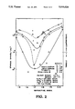
- the amount of compressive/tensile stress contained in the layer may be adjusted during the formation of the layer by adjustment of the pressure in accordance with the parameters shown in ASM America Newsletter, Volume 1, No. 1 of December, 1985, cross-reference to which is hereby made, and the graph shown in FIG. 2. It will be seen in that graph that the use of higher pressure, i.e., greater than about 1.5 Torr, will result in a shift in the stress into a tensile stress mode.
- the amount of pressure used, and the resulting amount of either compressive or tensile stress formed in the intermediate layer will be empirically determined, in part, by the amount of compressive stress formed in the subsequently formed silicon nitride layer to result in a composite layer having a compressive/tensile stress which will usually-still, be on the compressive side but will be insufficient to result in the formation of voids in the underlying metal layer.
- the amount of compressive stress developed in the silicon oxynitride layer may also be lowered by adjusting other parameters in the reaction process such as by lowering the RF power in the plasma deposition reactor, e.g., from a normal 1500 watts, or lowering the duty cycle of the RF power which results in the appearance of operating at a lower power.
- the amount of NO 2 gas used may also be increased to lower the compressive stress of the silicon oxynitride layer.
- Other known reaction parameters which may also have an effect on the resulting compressive stress and which are interrelated to those just mentioned such as reaction time and flow rates may also be modified as well to achieve the desired compressive/tensile stress in the silicon oxynitride layer.
- the compressive/tensile stress on the intermediate layer should be adjusted as much as possible without increasing tensile stress sufficiently to result in die cracking.
- This again will be an empirical determination since the amount of tensile stress which may be applied to the intermediate layer without resulting in cracking of the die will depend upon other processing steps as well as the geometry of the particular die.
- one skilled in the art will be able to readily determine, in the finished product, whether too much tensile stress has been applied to the intermediate layer resulting in cracking of the die.
- the amount of compressive stress formed in the silicon nitride layer may also be controlled to some extent by adjustment of the pressure, i.e., by raising the pressure, during formation of the silicon nitride layer.
- adjustment of the pressure i.e., by raising the pressure
- the ultimate reason for using a silicon nitride encapsulation or passivation layer is the superior moisture and ion penetration resistance of the silicon nitride layer over layers of other material such as silicon oxide and silicon oxynitride.
- Modification of the silicon nitride layer to relieve stress in the metal layer is, furthermore, a particular problem in application of the silicon nitride layer as an encapsulant for EPROMS, both due to the need for preserving UV transparency (which is related to the amount of compressive stress and which, prior to the aforesaid Forouhi et al '541 patent, was a problem in itself to achieve) and preserving the resistance to moisture penetration since an EPROM structure is particularly sensitive to moisture.
- This resistance to moisture and ion penetration is achieved by forming the silicon nitride layer in a compressive stress mode. While all compressive stress, therefore, could probably be alleviated or removed by adjustment of the reaction parameters, such as by providing higher pressure or lower RF power during formation of the silicon nitride film, such would be at the expense of the excellent moisture and ion penetration resistance of the silicon nitride layer which would be counter productive. Thus the amount of pressure increase during the formation of the silicon nitride layer will, in accordance with the invention, be insufficient to remove the resulting silicon nitride layer from a compressive stress mode. More particularly, the compressive stress remaining on the silicon nitride layer should not be less than about 2.5 ⁇ 10 9 dynes/cm 2 , preferably 5 ⁇ 10 9 dynes/cm 2 .
- the amount of compressive stress remaining may be further characterized as providing the UV light transparency at 2537 ⁇ wavelength indicated by at least a 3% reflectance value as measured, for example, by a Hewlett-Packard Diode Array Spectrophotometer Model No. 8450A and preferably sufficient UV light transparency to permit erasure of the EPROM with a dual layer film (silicon oxynitride-silicon nitride) in less than one hour at 0.02-0.03 watts/cm 2 using, for example, a Spectronic UV light eraser.
- control and adjustment of the reaction parameters during formation of the silicon nitride layer which affect the compressive stress developed by the layer will, in accordance with the invention, always be done in combination with either or both of the other aspects of the invention, i.e., in combination with the treatment of the metal surface or the formation of the intermediate layer or both so as to not lose the excellent moisture and ion penetration resistance properties of the silicon nitride layer.
- the hierarchy of treatments steps will favor utilizing one or both of the first two treatments prior to lowering the compressive stress on the silicon nitride layer to lower the risk of loss of some of the excellent moisture and ion penetration resistance which characterizes a silicon nitride layer under compressive stress. Therefore, before lowering the compressive stress of the silicon nitride layer, at least one or the other of the first two steps should be performed. Furthermore, with respect to the lowering of the compressive stress of the intermediate layer, the compressive/tensile stress on the intermediate layer should be adjusted, as discussed above, as much as possible without increasing tensile stress sufficiently to result in die cracking.
- the amount of adjustment of the compressive stress of the silicon nitride layer should, therefore, be insufficient to measurably increase the penetration of moisture or ion contaminates through the layer.
- the change in reaction conditions resulting in lowering of the compressive stress of the silicon nitride layer e.g., raising the pressure in the PECVD system used to form the silicon nitride layer, should only be made sufficiently to result in the elimination of voids in the metal layer, and such process adjustments should only be done after at least one of the other steps has been carried out to avoid an excessive loss of compressive stress in the silicon nitride layer and resultant loss of moisture and ion penetration resistance.
- the amount of decrease in the compressive stress of the silicon nitride layer should also be insufficient to interfere with the transparency of the silicon nitride layer.
- an integrated. circuit structure having a patterned aluminum layer thereon was subject to an argon implantation at an energy level of 70 kEV at ambient temperature to provide an implantation of about 5 ⁇ 10 15 ions/cm 2 to a depth of about 750 ⁇ in the aluminum surface.
- a silicon oxynitride layer of about 1.35 micron thickness was then formed over the implanted aluminum layer in a plasma enhanced chemical vacuum deposition (PECVD) apparatus comprising a 1500 watt ASM Micon V plasma deposition reactor and using a duty cycle of 30 milliseconds on and 300 milliseconds off.
- the reactants comprised a mixture of 400 SCCM silane (SiH 4 ), 3000 SCCM NH 3 , and 2000 SCCM N 2 O and were flowed over the structure in a vacuum chamber maintained at 380° C. and a pressure of 1.6 Torr to provide a deposition rate of about 200 ⁇ /minute.
- the deposition was carried out for 68 minutes to yield a silicon oxynitride layer having a tensile stress of 5 ⁇ 10 8 dynes/cm 2 as measured with an IONIC stress gauge.
- a silicon nitride layer transparent to UV radiation at 2537 ⁇ was then formed over the silicon oxynitride layer using the process of the Forouhi et al '541 patent modified somewhat to reduce the compressive stress in the silicon nitride layer using the same type of plasma enhanced chemical vacuum deposition (PECVD) apparatus as used to form the silicon oxynitride layer, i.e., a 1500 watt ASM Micon V plasma deposition reactor using a duty cycle of 30 milliseconds on and 300 milliseconds off.
- a gas flow of 300 SCCM silane to 5300 SCCM ammonia was used at a temperature of about 380° C. and a pressure of about 2.0 Torr.
- the PECVD deposition was carried out for about 105 minutes to form a silicon nitride layer of about 1.35 micron thickness having a compressive stress of 5 ⁇ 10 9 dynes/cm 2 as measured with an IONIC stress gauge.
- the integrated circuit structure was visually examined under a microscope for voids. None were seen.
- the structure was then placed in a furnace and heated to 400° C. and maintained at this temperature for 20 minutes in a nitrogen atmosphere.
- the structure was removed from the furnace and again examined under a microscope. Again no voids were noted.
- the structure was then completed and placed in an oven and heated to 200° C. and held at this temperature for 20 hours in a nitrogen atmosphere.
- the structure was removed from the oven and again examined for voids under a microscope. No voids were found in the aluminum portion examined.
- the invention provides a method for the production of an integrated circuit structure encapsulated by a silicon nitride layer to provide excellent resistance to moisture and ion penetration while providing sufficient stress relief in and adjacent the underlying metal layer to prevent the formation of undesirable voids in the underlying metal layer.
Abstract
Description
Claims (30)
Priority Applications (1)
| Application Number | Priority Date | Filing Date | Title |
|---|---|---|---|
| US07/353,169 US5010024A (en) | 1987-03-04 | 1989-05-15 | Passivation for integrated circuit structures |
Applications Claiming Priority (2)
| Application Number | Priority Date | Filing Date | Title |
|---|---|---|---|
| US2182887A | 1987-03-04 | 1987-03-04 | |
| US07/353,169 US5010024A (en) | 1987-03-04 | 1989-05-15 | Passivation for integrated circuit structures |
Related Parent Applications (1)
| Application Number | Title | Priority Date | Filing Date |
|---|---|---|---|
| US2182887A Division | 1987-03-04 | 1987-03-04 |
Publications (1)
| Publication Number | Publication Date |
|---|---|
| US5010024A true US5010024A (en) | 1991-04-23 |
Family
ID=26695147
Family Applications (1)
| Application Number | Title | Priority Date | Filing Date |
|---|---|---|---|
| US07/353,169 Expired - Lifetime US5010024A (en) | 1987-03-04 | 1989-05-15 | Passivation for integrated circuit structures |
Country Status (1)
| Country | Link |
|---|---|
| US (1) | US5010024A (en) |
Cited By (45)
| Publication number | Priority date | Publication date | Assignee | Title |
|---|---|---|---|---|
| US5279981A (en) * | 1991-04-15 | 1994-01-18 | Nippondenso Co., Ltd. | Method of reducing the trap density of an oxide film for application to fabricating a nonvolatile memory cell |
| US5334555A (en) * | 1991-11-06 | 1994-08-02 | Sony Corporation | Method of determining conditions for plasma silicon nitride film growth and method of manufacturing semiconductor device |
| US5744378A (en) * | 1993-12-14 | 1998-04-28 | Nec Corporation | Method for fabricating a semiconductor device having multilevel interconnections |
| US5780891A (en) * | 1994-12-05 | 1998-07-14 | Micron Technology, Inc. | Nonvolatile floating gate memory with improved interploy dielectric |
| US5811316A (en) * | 1989-03-20 | 1998-09-22 | Hitachi. Ltd. | Method of forming teos oxide and silicon nitride passivation layer on aluminum wiring |
| US5883001A (en) * | 1994-11-07 | 1999-03-16 | Macronix International Co., Ltd. | Integrated circuit passivation process and structure |
| US5924001A (en) * | 1998-01-08 | 1999-07-13 | Taiwan Semiconductor Manufacturing Company, Ltd. | Ion implantation for preventing polycide void |
| US5939750A (en) * | 1998-01-21 | 1999-08-17 | Advanced Micro Devices | Use of implanted ions to reduce oxide-nitride-oxide (ONO) etch residue and polystringers |
| US5939333A (en) * | 1996-05-30 | 1999-08-17 | Micron Technology, Inc. | Silicon nitride deposition method |
| US6168983B1 (en) | 1996-11-05 | 2001-01-02 | Power Integrations, Inc. | Method of making a high-voltage transistor with multiple lateral conduction layers |
| US6174743B1 (en) * | 1998-12-08 | 2001-01-16 | Advanced Micro Devices, Inc. | Method of reducing incidence of stress-induced voiding in semiconductor interconnect lines |
| US6207994B1 (en) | 1996-11-05 | 2001-03-27 | Power Integrations, Inc. | High-voltage transistor with multi-layer conduction region |
| US6221794B1 (en) * | 1998-12-08 | 2001-04-24 | Advanced Micro Devices, Inc. | Method of reducing incidence of stress-induced voiding in semiconductor interconnect lines |
| US6316820B1 (en) | 1997-07-25 | 2001-11-13 | Hughes Electronics Corporation | Passivation layer and process for semiconductor devices |
| US6335533B1 (en) | 1998-12-07 | 2002-01-01 | Advanced Micro Devices, Inc. | Electron microscopy sample having silicon nitride passivation layer |
| US6350651B1 (en) * | 1999-06-10 | 2002-02-26 | Intel Corporation | Method for making flash memory with UV opaque passivation layer |
| US20020132465A1 (en) * | 1997-04-04 | 2002-09-19 | Elm Technology Corporation | Reconfigurable integrated circuit memory |
| US20020153556A1 (en) * | 1996-11-05 | 2002-10-24 | Power Integrations, Inc. | Method of making a high-voltage transistor with buried conduction regions |
| US20020179908A1 (en) * | 2001-04-27 | 2002-12-05 | Semiconductor Energy Laboratory Co., Ltd., | Semiconductor device and method of manufacturing the same |
| US6501130B2 (en) | 2001-01-24 | 2002-12-31 | Power Integrations, Inc. | High-voltage transistor with buried conduction layer |
| US6509220B2 (en) | 2000-11-27 | 2003-01-21 | Power Integrations, Inc. | Method of fabricating a high-voltage transistor |
| US20030047769A1 (en) * | 2001-09-07 | 2003-03-13 | Power Integrations, Inc. | High-voltage vertical transistor with a multi-layered extended drain structure |
| US20030047792A1 (en) * | 2001-09-07 | 2003-03-13 | Power Integrations, Inc. | High-voltage lateral transistor with a multi-layered extended drain structure |
| US20030057524A1 (en) * | 2001-09-07 | 2003-03-27 | Power Integrations, Inc. | Method of fabricating a high-voltage transistor with a multi-layered extended drain structure |
| US20030218182A1 (en) * | 1992-04-08 | 2003-11-27 | Leedy Glenn J. | Strees-controlled dielectric integrated circuit |
| US20030223535A1 (en) * | 1992-04-08 | 2003-12-04 | Leedy Glenn Joseph | Lithography device for semiconductor circuit pattern generator |
| US20040097008A1 (en) * | 1997-04-04 | 2004-05-20 | Elm Technology Corporation | Three dimensional structure integrated circuit |
| US20040108071A1 (en) * | 2001-04-11 | 2004-06-10 | Thomas Wien | Label applicator and system |
| US6768171B2 (en) | 2000-11-27 | 2004-07-27 | Power Integrations, Inc. | High-voltage transistor with JFET conduction channels |
| US20050023656A1 (en) * | 2002-08-08 | 2005-02-03 | Leedy Glenn J. | Vertical system integration |
| US20050133858A1 (en) * | 2001-09-07 | 2005-06-23 | Power Integrations, Inc. | High-voltage vertical transistor with a multi-gradient drain doping profile |
| US20050224792A1 (en) * | 2004-04-09 | 2005-10-13 | Taiwan Semiconductor Manufacturing Co. | Novel test structure for speeding a stress-induced voiding test and method of using same |
| US20080197418A1 (en) * | 2007-02-16 | 2008-08-21 | Power Integrations, Inc. | Gate pullback at ends of high-voltage vertical transistor structure |
| US20080197417A1 (en) * | 2007-02-16 | 2008-08-21 | Power Integrations, Inc. | Segmented pillar layout for a high-voltage vertical transistor |
| US20080197397A1 (en) * | 2007-02-16 | 2008-08-21 | Power Integrations, Inc. | Checkerboarded high-voltage vertical transistor layout |
| US20080197406A1 (en) * | 2007-02-16 | 2008-08-21 | Power Integrations, Inc. | Sensing FET integrated with a high-voltage vertical transistor |
| US7439096B2 (en) * | 2001-02-21 | 2008-10-21 | Lucent Technologies Inc. | Semiconductor device encapsulation |
| US7468536B2 (en) | 2007-02-16 | 2008-12-23 | Power Integrations, Inc. | Gate metal routing for transistor with checkerboarded layout |
| US7786533B2 (en) | 2001-09-07 | 2010-08-31 | Power Integrations, Inc. | High-voltage vertical transistor with edge termination structure |
| CN1964002B (en) * | 2005-11-12 | 2010-09-29 | 应用材料公司 | Method for fabricating controlled stress silicon nitride films |
| US20130075740A1 (en) * | 2010-04-06 | 2013-03-28 | Electronic and Telecommunications Research Institu te | P-type oxide alloys based on copper oxides, tin oxides, tin-copper alloy oxides and metal alloy thereof, and nickel oxide, with embedded metals thereof, fabrication process and use thereof |
| US20130119282A1 (en) * | 2011-11-14 | 2013-05-16 | Stmicroelectronics Pte Ltd. | Wafer level packaging, optical detection sensor and method of forming same |
| US9543396B2 (en) | 2013-12-13 | 2017-01-10 | Power Integrations, Inc. | Vertical transistor device structure with cylindrically-shaped regions |
| US9660053B2 (en) | 2013-07-12 | 2017-05-23 | Power Integrations, Inc. | High-voltage field-effect transistor having multiple implanted layers |
| US10325988B2 (en) | 2013-12-13 | 2019-06-18 | Power Integrations, Inc. | Vertical transistor device structure with cylindrically-shaped field plates |
Citations (11)
| Publication number | Priority date | Publication date | Assignee | Title |
|---|---|---|---|---|
| US3660819A (en) * | 1970-06-15 | 1972-05-02 | Intel Corp | Floating gate transistor and method for charging and discharging same |
| JPS5556635A (en) * | 1978-10-20 | 1980-04-25 | Sanyo Electric Co Ltd | Preparation of surface top coat in semiconductor device |
| US4203158A (en) * | 1978-02-24 | 1980-05-13 | Intel Corporation | Electrically programmable and erasable MOS floating gate memory device employing tunneling and method of fabricating same |
| US4223048A (en) * | 1978-08-07 | 1980-09-16 | Pacific Western Systems | Plasma enhanced chemical vapor processing of semiconductive wafers |
| US4393479A (en) * | 1980-11-17 | 1983-07-12 | Texas Instruments Incorporated | Method for erasing data of a non-volatile semiconductor memory integrated circuit |
| US4406053A (en) * | 1980-07-31 | 1983-09-27 | Fujitsu Limited | Process for manufacturing a semiconductor device having a non-porous passivation layer |
| US4446194A (en) * | 1982-06-21 | 1984-05-01 | Motorola, Inc. | Dual layer passivation |
| US4448400A (en) * | 1981-07-13 | 1984-05-15 | Eliyahou Harari | Highly scalable dynamic RAM cell with self-signal amplification |
| US4516313A (en) * | 1983-05-27 | 1985-05-14 | Ncr Corporation | Unified CMOS/SNOS semiconductor fabrication process |
| US4532022A (en) * | 1979-09-14 | 1985-07-30 | Fujitsu Limited | Process of producing a semiconductor device |
| US4618541A (en) * | 1984-12-21 | 1986-10-21 | Advanced Micro Devices, Inc. | Method of forming a silicon nitride film transparent to ultraviolet radiation and resulting article |
-
1989
- 1989-05-15 US US07/353,169 patent/US5010024A/en not_active Expired - Lifetime
Patent Citations (12)
| Publication number | Priority date | Publication date | Assignee | Title |
|---|---|---|---|---|
| US3660819A (en) * | 1970-06-15 | 1972-05-02 | Intel Corp | Floating gate transistor and method for charging and discharging same |
| US4203158A (en) * | 1978-02-24 | 1980-05-13 | Intel Corporation | Electrically programmable and erasable MOS floating gate memory device employing tunneling and method of fabricating same |
| US4203158B1 (en) * | 1978-02-24 | 1992-09-22 | Intel Corp | |
| US4223048A (en) * | 1978-08-07 | 1980-09-16 | Pacific Western Systems | Plasma enhanced chemical vapor processing of semiconductive wafers |
| JPS5556635A (en) * | 1978-10-20 | 1980-04-25 | Sanyo Electric Co Ltd | Preparation of surface top coat in semiconductor device |
| US4532022A (en) * | 1979-09-14 | 1985-07-30 | Fujitsu Limited | Process of producing a semiconductor device |
| US4406053A (en) * | 1980-07-31 | 1983-09-27 | Fujitsu Limited | Process for manufacturing a semiconductor device having a non-porous passivation layer |
| US4393479A (en) * | 1980-11-17 | 1983-07-12 | Texas Instruments Incorporated | Method for erasing data of a non-volatile semiconductor memory integrated circuit |
| US4448400A (en) * | 1981-07-13 | 1984-05-15 | Eliyahou Harari | Highly scalable dynamic RAM cell with self-signal amplification |
| US4446194A (en) * | 1982-06-21 | 1984-05-01 | Motorola, Inc. | Dual layer passivation |
| US4516313A (en) * | 1983-05-27 | 1985-05-14 | Ncr Corporation | Unified CMOS/SNOS semiconductor fabrication process |
| US4618541A (en) * | 1984-12-21 | 1986-10-21 | Advanced Micro Devices, Inc. | Method of forming a silicon nitride film transparent to ultraviolet radiation and resulting article |
Non-Patent Citations (18)
| Title |
|---|
| "Controlling Stress in Oxy-Nitride Films", ASM America News Letter, vol. 1, No. 2, Dec. 1985, pp. 1-3. |
| Alexander, K. et al., "Moisture Resistive, UV Transmissive Passivation for Plastic Encapsulated EPROM Devices", IEEE 22nd Annual proceedings of the International Reliability Physics Symposium, Apr. 3-5, 1984, pp. 218-222. |
| Alexander, K. et al., Moisture Resistive, UV Transmissive Passivation for Plastic Encapsulated EPROM Devices , IEEE 22nd Annual proceedings of the International Reliability Physics Symposium, Apr. 3 5, 1984, pp. 218 222. * |
| Controlling Stress in Oxy Nitride Films , ASM America News Letter, vol. 1, No. 2, Dec. 1985, pp. 1 3. * |
| Frohman Bentchkowsky, D., FAMOS A New Semiconductor Charge Storage Device , Solid State Electronics, vol. 17, 1974, pp. 517 529. * |
| Frohman-Bentchkowsky, D., "FAMOS-A New Semiconductor Charge Storage Device", Solid State Electronics, vol. 17, 1974, pp. 517-529. |
| Katznelson, R. et al., "An Erase Model for FAMOS EPROM Devices", IEEE Transactions on Electron Devices, vol. ED-27, No. 9, Sep. 1980, pp. 1744-1752. |
| Katznelson, R. et al., An Erase Model for FAMOS EPROM Devices , IEEE Transactions on Electron Devices, vol. ED 27, No. 9, Sep. 1980, pp. 1744 1752. * |
| Nagy, T. E. et al., "Physical and Electrical Properties of Plasma Deposited Silicon Nitride Films", ECS Proceedings of the Symposium on Silicon Nitride Thin Insulating Films, vol. 83-8, 1983, pp. 167-176. |
| Nagy, T. E. et al., Physical and Electrical Properties of Plasma Deposited Silicon Nitride Films , ECS Proceedings of the Symposium on Silicon Nitride Thin Insulating Films, vol. 83 8, 1983, pp. 167 176. * |
| Rand, M. J. et al., "Optical Absorption as a Control Test for Plasma Silicon Nitride Deposition", Journal of the Electrochemical Society: Solid-State and Technology, vol. 125, No. 1, Jan., 1978, pp. 99-101. |
| Rand, M. J. et al., Optical Absorption as a Control Test for Plasma Silicon Nitride Deposition , Journal of the Electrochemical Society: Solid State and Technology, vol. 125, No. 1, Jan., 1978, pp. 99 101. * |
| Samuelson, G. M. et al., "The Correlations Between Physical and Electrical Properties of PECVO SiN with their Composition Ratios", Journal of the Electrochemical Society: Solid State Science and Technology, vol. 129, No. 8, Aug. 1982, pp. 1773-1778. |
| Samuelson, G. M. et al., The Correlations Between Physical and Electrical Properties of PECVO SiN with their Composition Ratios , Journal of the Electrochemical Society: Solid State Science and Technology, vol. 129, No. 8, Aug. 1982, pp. 1773 1778. * |
| Sinha, A. K. et al., "Reactive Plasma Deposited SiN Films for MOS-LSI Passivation", Journal of the Electrochemical Society: Solid State Science and Technology, vol. 125, No. 4, Apr. 1978, pp. 601-608. |
| Sinha, A. K. et al., Reactive Plasma Deposited SiN Films for MOS LSI Passivation , Journal of the Electrochemical Society: Solid State Science and Technology, vol. 125, No. 4, Apr. 1978, pp. 601 608. * |
| Yue, J. T. et al., "Stress Induced Voids in Aluminum Interconnects During IC Processing", IEEE 23rd International Reliability Physics Symposium, 1985, pp. 126-137. |
| Yue, J. T. et al., Stress Induced Voids in Aluminum Interconnects During IC Processing , IEEE 23rd International Reliability Physics Symposium, 1985, pp. 126 137. * |
Cited By (186)
| Publication number | Priority date | Publication date | Assignee | Title |
|---|---|---|---|---|
| US6894334B2 (en) | 1989-03-20 | 2005-05-17 | Hitachi, Ltd. | Semiconductor integrated circuit device, process for fabricating the same, and apparatus for fabricating the same |
| US6127255A (en) * | 1989-03-20 | 2000-10-03 | Hitachi, Ltd. | Semiconductor integrated circuit device, process for fabricating the same, and apparatus for fabricating the same |
| US20030189255A1 (en) * | 1989-03-20 | 2003-10-09 | Jun Sugiura | Semiconductor integrated circuit device, process for fabricating the same, and apparatus for fabricating the same |
| US6342412B1 (en) | 1989-03-20 | 2002-01-29 | Hitachi, Ltd. | Semiconductor integrated circuit device, process for fabricating the same, and apparatus for fabricating the same |
| US5811316A (en) * | 1989-03-20 | 1998-09-22 | Hitachi. Ltd. | Method of forming teos oxide and silicon nitride passivation layer on aluminum wiring |
| US6548847B2 (en) | 1989-03-20 | 2003-04-15 | Hitachi, Ltd. | Semiconductor integrated circuit device having a first wiring strip exposed through a connecting hole, a transition-metal film in the connecting hole and an aluminum wiring strip thereover, and a transition-metal nitride film between the aluminum wiring strip and the transition-metal film |
| US6169324B1 (en) | 1989-03-20 | 2001-01-02 | Hitachi, Ltd. | Semiconductor integrated circuit device, process for fabricating the same, and apparatus for fabricating the same |
| US5279981A (en) * | 1991-04-15 | 1994-01-18 | Nippondenso Co., Ltd. | Method of reducing the trap density of an oxide film for application to fabricating a nonvolatile memory cell |
| US5334555A (en) * | 1991-11-06 | 1994-08-02 | Sony Corporation | Method of determining conditions for plasma silicon nitride film growth and method of manufacturing semiconductor device |
| US20040132303A1 (en) * | 1992-04-08 | 2004-07-08 | Elm Technology Corporation | Membrane 3D IC fabrication |
| US20040192045A1 (en) * | 1992-04-08 | 2004-09-30 | Elm Technology Corporation. | Apparatus and methods for maskless pattern generation |
| US20030223535A1 (en) * | 1992-04-08 | 2003-12-04 | Leedy Glenn Joseph | Lithography device for semiconductor circuit pattern generator |
| US7763948B2 (en) | 1992-04-08 | 2010-07-27 | Taiwan Semiconductor Manufacturing Co., Ltd. | Flexible and elastic dielectric integrated circuit |
| US6682981B2 (en) | 1992-04-08 | 2004-01-27 | Elm Technology Corporation | Stress controlled dielectric integrated circuit fabrication |
| US7670893B2 (en) | 1992-04-08 | 2010-03-02 | Taiwan Semiconductor Manufacturing Co., Ltd. | Membrane IC fabrication |
| US6713327B2 (en) | 1992-04-08 | 2004-03-30 | Elm Technology Corporation | Stress controlled dielectric integrated circuit fabrication |
| US6765279B2 (en) | 1992-04-08 | 2004-07-20 | Elm Technology Corporation | Membrane 3D IC fabrication |
| US7615837B2 (en) | 1992-04-08 | 2009-11-10 | Taiwan Semiconductor Manufacturing Company | Lithography device for semiconductor circuit pattern generation |
| US7550805B2 (en) | 1992-04-08 | 2009-06-23 | Elm Technology Corporation | Stress-controlled dielectric integrated circuit |
| US20040150068A1 (en) * | 1992-04-08 | 2004-08-05 | Elm Technology Corporation | Membrane 3D IC fabrication |
| US7485571B2 (en) | 1992-04-08 | 2009-02-03 | Elm Technology Corporation | Method of making an integrated circuit |
| US7479694B2 (en) | 1992-04-08 | 2009-01-20 | Elm Technology Corporation | Membrane 3D IC fabrication |
| US20030218182A1 (en) * | 1992-04-08 | 2003-11-27 | Leedy Glenn J. | Strees-controlled dielectric integrated circuit |
| US7820469B2 (en) | 1992-04-08 | 2010-10-26 | Taiwan Semiconductor Manufacturing Co., Ltd. | Stress-controlled dielectric integrated circuit |
| US7242012B2 (en) | 1992-04-08 | 2007-07-10 | Elm Technology Corporation | Lithography device for semiconductor circuit pattern generator |
| US7385835B2 (en) | 1992-04-08 | 2008-06-10 | Elm Technology Corporation | Membrane 3D IC fabrication |
| US7307020B2 (en) | 1992-04-08 | 2007-12-11 | Elm Technology Corporation | Membrane 3D IC fabrication |
| US20080302559A1 (en) * | 1992-04-08 | 2008-12-11 | Elm Technology Corporation | Flexible and elastic dielectric integrated circuit |
| US7223696B2 (en) | 1992-04-08 | 2007-05-29 | Elm Technology Corporation | Methods for maskless lithography |
| US7176545B2 (en) | 1992-04-08 | 2007-02-13 | Elm Technology Corporation | Apparatus and methods for maskless pattern generation |
| US20050176174A1 (en) * | 1992-04-08 | 2005-08-11 | Elm Technology Corporation | Methodof making an integrated circuit |
| US20050156265A1 (en) * | 1992-04-08 | 2005-07-21 | Elm Technology Corporation | Lithography device for semiconductor circuit pattern generation |
| US20050130351A1 (en) * | 1992-04-08 | 2005-06-16 | Elm Technology Corporation | Methods for maskless lithography |
| US7911012B2 (en) | 1992-04-08 | 2011-03-22 | Taiwan Semiconductor Manufacturing Co., Ltd. | Flexible and elastic dielectric integrated circuit |
| US20050082641A1 (en) * | 1992-04-08 | 2005-04-21 | Elm Technology Corporation | Flexible and elastic dielectric integrated circuit |
| US20050082626A1 (en) * | 1992-04-08 | 2005-04-21 | Elm Technology Corporation | Membrane 3D IC fabrication |
| US20040197951A1 (en) * | 1992-04-08 | 2004-10-07 | Leedy Glenn Joseph | Membrane IC fabrication |
| US5744378A (en) * | 1993-12-14 | 1998-04-28 | Nec Corporation | Method for fabricating a semiconductor device having multilevel interconnections |
| US5883001A (en) * | 1994-11-07 | 1999-03-16 | Macronix International Co., Ltd. | Integrated circuit passivation process and structure |
| US6274902B1 (en) | 1994-12-05 | 2001-08-14 | Micron Technology, Inc. | Nonvolatile floating gate memory with improved interpoly dielectric |
| US6177311B1 (en) | 1994-12-05 | 2001-01-23 | Micron Technology, Inc. | Method for making a floating gate memory with improved interpoly dielectric |
| US6157059A (en) * | 1994-12-05 | 2000-12-05 | Micron Technology, Inc. | Nonvolatile floating gate memory with improved interpoly dielectric |
| US5780891A (en) * | 1994-12-05 | 1998-07-14 | Micron Technology, Inc. | Nonvolatile floating gate memory with improved interploy dielectric |
| US6127287A (en) * | 1996-05-30 | 2000-10-03 | Micron Technology, Inc. | Silicon nitride deposition method for use in forming a memory cell dielectric |
| US6204206B1 (en) | 1996-05-30 | 2001-03-20 | Micron Technology, Inc. | Silicon nitride deposition method |
| US6350708B1 (en) | 1996-05-30 | 2002-02-26 | Micron Technology, Inc. | Silicon nitride deposition method |
| US5939333A (en) * | 1996-05-30 | 1999-08-17 | Micron Technology, Inc. | Silicon nitride deposition method |
| US6633065B2 (en) | 1996-11-05 | 2003-10-14 | Power Integrations, Inc. | High-voltage transistor with multi-layer conduction region |
| US6768172B2 (en) | 1996-11-05 | 2004-07-27 | Power Integrations, Inc. | High-voltage transistor with multi-layer conduction region |
| US6639277B2 (en) | 1996-11-05 | 2003-10-28 | Power Integrations, Inc. | High-voltage transistor with multi-layer conduction region |
| US6207994B1 (en) | 1996-11-05 | 2001-03-27 | Power Integrations, Inc. | High-voltage transistor with multi-layer conduction region |
| US20030151101A1 (en) * | 1996-11-05 | 2003-08-14 | Power Integrations, Inc. | High-voltage transistor with multi-layer conduction region |
| US20020153556A1 (en) * | 1996-11-05 | 2002-10-24 | Power Integrations, Inc. | Method of making a high-voltage transistor with buried conduction regions |
| US20030151093A1 (en) * | 1996-11-05 | 2003-08-14 | Power Integrations, Inc. | High-voltage transistor with multi-layer conduction region |
| US6168983B1 (en) | 1996-11-05 | 2001-01-02 | Power Integrations, Inc. | Method of making a high-voltage transistor with multiple lateral conduction layers |
| US6828631B2 (en) | 1996-11-05 | 2004-12-07 | Power Integrations, Inc | High-voltage transistor with multi-layer conduction region |
| US20040217419A1 (en) * | 1996-11-05 | 2004-11-04 | Power Integrations, Inc. | High-voltage transistor with multi-layer conduction region |
| US6724041B2 (en) | 1996-11-05 | 2004-04-20 | Power Integrations, Inc. | Method of making a high-voltage transistor with buried conduction regions |
| US20040207012A1 (en) * | 1996-11-05 | 2004-10-21 | Power Integrations, Inc. | High-voltage transistor with multi-layer conduction region |
| US6800903B2 (en) | 1996-11-05 | 2004-10-05 | Power Integrations, Inc. | High-voltage transistor with multi-layer conduction region |
| US6787437B2 (en) | 1996-11-05 | 2004-09-07 | Power Integrations, Inc. | Method of making a high-voltage transistor with buried conduction regions |
| US6777749B2 (en) | 1996-11-05 | 2004-08-17 | Power Integrations, Inc. | High-voltage transistor with multi-layer conduction region |
| US6570219B1 (en) | 1996-11-05 | 2003-05-27 | Power Integrations, Inc. | High-voltage transistor with multi-layer conduction region |
| US8410617B2 (en) | 1997-04-04 | 2013-04-02 | Elm Technology | Three dimensional structure memory |
| US9401183B2 (en) | 1997-04-04 | 2016-07-26 | Glenn J. Leedy | Stacked integrated memory device |
| US8933570B2 (en) | 1997-04-04 | 2015-01-13 | Elm Technology Corp. | Three dimensional structure memory |
| US20040151043A1 (en) * | 1997-04-04 | 2004-08-05 | Elm Technology Corporation | Three dimensional structure memory |
| US9087556B2 (en) | 1997-04-04 | 2015-07-21 | Glenn J Leedy | Three dimension structure memory |
| US8928119B2 (en) | 1997-04-04 | 2015-01-06 | Glenn J. Leedy | Three dimensional structure memory |
| US8907499B2 (en) | 1997-04-04 | 2014-12-09 | Glenn J Leedy | Three dimensional structure memory |
| US7474004B2 (en) | 1997-04-04 | 2009-01-06 | Elm Technology Corporation | Three dimensional structure memory |
| US8841778B2 (en) | 1997-04-04 | 2014-09-23 | Glenn J Leedy | Three dimensional memory structure |
| US8824159B2 (en) | 1997-04-04 | 2014-09-02 | Glenn J. Leedy | Three dimensional structure memory |
| US7705466B2 (en) | 1997-04-04 | 2010-04-27 | Elm Technology Corporation | Three dimensional multi layer memory and control logic integrated circuit structure |
| US20030057564A1 (en) * | 1997-04-04 | 2003-03-27 | Elm Technology Corporation | Three dimensional structure memory |
| US20040097008A1 (en) * | 1997-04-04 | 2004-05-20 | Elm Technology Corporation | Three dimensional structure integrated circuit |
| US20040070063A1 (en) * | 1997-04-04 | 2004-04-15 | Elm Technology Corporation | Three dimensional structure integrated circuit |
| US8796862B2 (en) | 1997-04-04 | 2014-08-05 | Glenn J Leedy | Three dimensional memory structure |
| US20090067210A1 (en) * | 1997-04-04 | 2009-03-12 | Leedy Glenn J | Three dimensional structure memory |
| US8791581B2 (en) | 1997-04-04 | 2014-07-29 | Glenn J Leedy | Three dimensional structure memory |
| US7193239B2 (en) | 1997-04-04 | 2007-03-20 | Elm Technology Corporation | Three dimensional structure integrated circuit |
| US7504732B2 (en) | 1997-04-04 | 2009-03-17 | Elm Technology Corporation | Three dimensional structure memory |
| US8629542B2 (en) | 1997-04-04 | 2014-01-14 | Glenn J. Leedy | Three dimensional structure memory |
| US20090175104A1 (en) * | 1997-04-04 | 2009-07-09 | Leedy Glenn J | Three dimensional structure memory |
| US8318538B2 (en) | 1997-04-04 | 2012-11-27 | Elm Technology Corp. | Three dimensional structure memory |
| US8288206B2 (en) | 1997-04-04 | 2012-10-16 | Elm Technology Corp | Three dimensional structure memory |
| US8035233B2 (en) | 1997-04-04 | 2011-10-11 | Elm Technology Corporation | Adjacent substantially flexible substrates having integrated circuits that are bonded together by non-polymeric layer |
| US20100171224A1 (en) * | 1997-04-04 | 2010-07-08 | Leedy Glenn J | Three dimensional structure memory |
| US20090218700A1 (en) * | 1997-04-04 | 2009-09-03 | Leedy Glenn J | Three dimensional structure memory |
| US20090219744A1 (en) * | 1997-04-04 | 2009-09-03 | Leedy Glenn J | Three dimensional structure memory |
| US20090219743A1 (en) * | 1997-04-04 | 2009-09-03 | Leedy Glenn J | Three dimensional structure memory |
| US7138295B2 (en) | 1997-04-04 | 2006-11-21 | Elm Technology Corporation | Method of information processing using three dimensional integrated circuits |
| US20020132465A1 (en) * | 1997-04-04 | 2002-09-19 | Elm Technology Corporation | Reconfigurable integrated circuit memory |
| US20100173453A1 (en) * | 1997-04-04 | 2010-07-08 | Leedy Glenn J | Three dimensional structure memory |
| US20030173608A1 (en) * | 1997-04-04 | 2003-09-18 | Elm Technology Corporation | Three dimensional structure integrated circuit |
| US6504235B2 (en) | 1997-07-25 | 2003-01-07 | Hughes Electronics Corporation | Passivation layer and process for semiconductor devices |
| US6316820B1 (en) | 1997-07-25 | 2001-11-13 | Hughes Electronics Corporation | Passivation layer and process for semiconductor devices |
| US5924001A (en) * | 1998-01-08 | 1999-07-13 | Taiwan Semiconductor Manufacturing Company, Ltd. | Ion implantation for preventing polycide void |
| US5939750A (en) * | 1998-01-21 | 1999-08-17 | Advanced Micro Devices | Use of implanted ions to reduce oxide-nitride-oxide (ONO) etch residue and polystringers |
| US6335533B1 (en) | 1998-12-07 | 2002-01-01 | Advanced Micro Devices, Inc. | Electron microscopy sample having silicon nitride passivation layer |
| US6174743B1 (en) * | 1998-12-08 | 2001-01-16 | Advanced Micro Devices, Inc. | Method of reducing incidence of stress-induced voiding in semiconductor interconnect lines |
| US6221794B1 (en) * | 1998-12-08 | 2001-04-24 | Advanced Micro Devices, Inc. | Method of reducing incidence of stress-induced voiding in semiconductor interconnect lines |
| US6849896B2 (en) | 1999-06-10 | 2005-02-01 | Intel Corporation | Flash memory with UV opaque passivation layer |
| US6350651B1 (en) * | 1999-06-10 | 2002-02-26 | Intel Corporation | Method for making flash memory with UV opaque passivation layer |
| US20020094595A1 (en) * | 1999-06-10 | 2002-07-18 | Glen Wada | Method for making flash memory with UV opaque passivation layer |
| US6768171B2 (en) | 2000-11-27 | 2004-07-27 | Power Integrations, Inc. | High-voltage transistor with JFET conduction channels |
| US6509220B2 (en) | 2000-11-27 | 2003-01-21 | Power Integrations, Inc. | Method of fabricating a high-voltage transistor |
| US6818490B2 (en) | 2001-01-24 | 2004-11-16 | Power Integrations, Inc. | Method of fabricating complementary high-voltage field-effect transistors |
| US6504209B2 (en) | 2001-01-24 | 2003-01-07 | Power Integrations, Inc. | High-voltage transistor with buried conduction layer |
| US20040036115A1 (en) * | 2001-01-24 | 2004-02-26 | Power Integrations, Inc. | High-voltage transistor with buried conduction layer |
| US6501130B2 (en) | 2001-01-24 | 2002-12-31 | Power Integrations, Inc. | High-voltage transistor with buried conduction layer |
| US7439096B2 (en) * | 2001-02-21 | 2008-10-21 | Lucent Technologies Inc. | Semiconductor device encapsulation |
| US7302982B2 (en) | 2001-04-11 | 2007-12-04 | Avery Dennison Corporation | Label applicator and system |
| US20040108071A1 (en) * | 2001-04-11 | 2004-06-10 | Thomas Wien | Label applicator and system |
| US7132317B2 (en) * | 2001-04-27 | 2006-11-07 | Semiconductor Energy Laboratory Co., Ltd. | Method of manufacturing a semiconductor device that includes changing the internal stress of a conductive film |
| US9997543B2 (en) | 2001-04-27 | 2018-06-12 | Semiconductor Energy Laboratory Co., Ltd. | Semiconductor device and method of manufacturing the same |
| US20020179908A1 (en) * | 2001-04-27 | 2002-12-05 | Semiconductor Energy Laboratory Co., Ltd., | Semiconductor device and method of manufacturing the same |
| US20070065995A1 (en) * | 2001-04-27 | 2007-03-22 | Semiconductor Energy Laboratory Co., Ltd. | Semiconductor device and method of manufacturing the same |
| US9362273B2 (en) | 2001-04-27 | 2016-06-07 | Semiconductor Energy Laboratory Co., Ltd. | Semiconductor device and method of manufacturing the same |
| US20110018058A1 (en) * | 2001-09-07 | 2011-01-27 | Power Integrations, Inc. | High-voltage vertical transistor with edge termination structure |
| US6815293B2 (en) | 2001-09-07 | 2004-11-09 | Power Intergrations, Inc. | High-voltage lateral transistor with a multi-layered extended drain structure |
| US6667213B2 (en) | 2001-09-07 | 2003-12-23 | Power Integrations, Inc. | Method of fabricating a high-voltage transistor with a multi-layered extended drain structure |
| US20030151110A1 (en) * | 2001-09-07 | 2003-08-14 | Power Integrations, Inc. | High-voltage lateral transistor with a multi-layered extended drain structure |
| US6750105B2 (en) | 2001-09-07 | 2004-06-15 | Power Integrations, Inc. | Method of fabricating a high-voltage transistor with a multi-layered extended drain structure |
| US6573558B2 (en) | 2001-09-07 | 2003-06-03 | Power Integrations, Inc. | High-voltage vertical transistor with a multi-layered extended drain structure |
| US8940605B2 (en) | 2001-09-07 | 2015-01-27 | Power Integrations, Inc. | Method of fabricating a high-voltage transistor with an extended drain structure |
| US6555873B2 (en) | 2001-09-07 | 2003-04-29 | Power Integrations, Inc. | High-voltage lateral transistor with a multi-layered extended drain structure |
| US6781198B2 (en) | 2001-09-07 | 2004-08-24 | Power Integrations, Inc. | High-voltage vertical transistor with a multi-layered extended drain structure |
| US6787847B2 (en) | 2001-09-07 | 2004-09-07 | Power Integrations, Inc. | High-voltage vertical transistor with a multi-layered extended drain structure |
| US6798020B2 (en) * | 2001-09-07 | 2004-09-28 | Power Integrations, Inc. | High-voltage lateral transistor with a multi-layered extended drain structure |
| US20030057524A1 (en) * | 2001-09-07 | 2003-03-27 | Power Integrations, Inc. | Method of fabricating a high-voltage transistor with a multi-layered extended drain structure |
| US7459366B2 (en) | 2001-09-07 | 2008-12-02 | Power Integrations, Inc. | High-voltage vertical transistor with a multi-gradient drain doping profile |
| US20040232486A1 (en) * | 2001-09-07 | 2004-11-25 | Power Integrations, Inc. | High-voltage lateral transistor with a multi-layered extended drain structure |
| US20080102581A1 (en) * | 2001-09-07 | 2008-05-01 | Power Integrations, Inc. | High-voltage vertical transistor with a multi-gradient drain doping profile |
| US20070293002A1 (en) * | 2001-09-07 | 2007-12-20 | Power Intergrations, Inc. | Method of fabricating a high-voltage transistor with an extended drain structure |
| US20090233407A1 (en) * | 2001-09-07 | 2009-09-17 | Power Integrations, Inc. | Method of fabricating a high-voltage transistor with an extended drain structure |
| US20050023571A1 (en) * | 2001-09-07 | 2005-02-03 | Power Integrations, Inc. | High-voltage vertical transistor with a multi-layered extended drain structure |
| US7253042B2 (en) | 2001-09-07 | 2007-08-07 | Power Integrations, Inc. | Method of fabricating a high-voltage transistor with an extended drain structure |
| US7221011B2 (en) | 2001-09-07 | 2007-05-22 | Power Integrations, Inc. | High-voltage vertical transistor with a multi-gradient drain doping profile |
| US8552496B2 (en) | 2001-09-07 | 2013-10-08 | Power Integrations, Inc. | High-voltage vertical transistor with edge termination structure |
| US7745291B2 (en) | 2001-09-07 | 2010-06-29 | Power Integrations, Inc. | Method of fabricating a high-voltage transistor with an extended drain structure |
| US20030047793A1 (en) * | 2001-09-07 | 2003-03-13 | Power Integrations, Inc. | High-voltage vertical transistor with a multi-layered extended drain structure |
| US6987299B2 (en) | 2001-09-07 | 2006-01-17 | Power Integrations, Inc. | High-voltage lateral transistor with a multi-layered extended drain structure |
| US20030047792A1 (en) * | 2001-09-07 | 2003-03-13 | Power Integrations, Inc. | High-voltage lateral transistor with a multi-layered extended drain structure |
| US7786533B2 (en) | 2001-09-07 | 2010-08-31 | Power Integrations, Inc. | High-voltage vertical transistor with edge termination structure |
| US20030047769A1 (en) * | 2001-09-07 | 2003-03-13 | Power Integrations, Inc. | High-voltage vertical transistor with a multi-layered extended drain structure |
| US20050133858A1 (en) * | 2001-09-07 | 2005-06-23 | Power Integrations, Inc. | High-voltage vertical transistor with a multi-gradient drain doping profile |
| US7829944B2 (en) | 2001-09-07 | 2010-11-09 | Power Integrations, Inc. | High-voltage vertical transistor with a multi-layered extended drain structure |
| US7998817B2 (en) | 2001-09-07 | 2011-08-16 | Power Integrations, Inc. | Method of fabricating a high-voltage transistor with an extended drain structure |
| US6635544B2 (en) | 2001-09-07 | 2003-10-21 | Power Intergrations, Inc. | Method of fabricating a high-voltage transistor with a multi-layered extended drain structure |
| US20050104121A1 (en) * | 2001-09-07 | 2005-05-19 | Power Integrations, Inc. | Method of fabricating a high-voltage transistor with an extended drain structure |
| US20050023656A1 (en) * | 2002-08-08 | 2005-02-03 | Leedy Glenn J. | Vertical system integration |
| US20080284611A1 (en) * | 2002-08-08 | 2008-11-20 | Elm Technology Corporation | Vertical system integration |
| US20080254572A1 (en) * | 2002-08-08 | 2008-10-16 | Elm Technology Corporation | Vertical system integration |
| US20080251941A1 (en) * | 2002-08-08 | 2008-10-16 | Elm Technology Corporation | Vertical system integration |
| US8080442B2 (en) | 2002-08-08 | 2011-12-20 | Elm Technology Corporation | Vertical system integration |
| US20080237591A1 (en) * | 2002-08-08 | 2008-10-02 | Elm Technology Corporation | Vertical system integration |
| US8269327B2 (en) | 2002-08-08 | 2012-09-18 | Glenn J Leedy | Vertical system integration |
| US20090194768A1 (en) * | 2002-08-08 | 2009-08-06 | Leedy Glenn J | Vertical system integration |
| US7402897B2 (en) | 2002-08-08 | 2008-07-22 | Elm Technology Corporation | Vertical system integration |
| US8587102B2 (en) | 2002-08-08 | 2013-11-19 | Glenn J Leedy | Vertical system integration |
| US7157925B2 (en) | 2004-04-09 | 2007-01-02 | Taiwan Semiconductor Manufacturing Co., Ltd. | Test structure for speeding a stress-induced voiding test and method of using same |
| US20050224792A1 (en) * | 2004-04-09 | 2005-10-13 | Taiwan Semiconductor Manufacturing Co. | Novel test structure for speeding a stress-induced voiding test and method of using same |
| US20070109008A1 (en) * | 2004-04-09 | 2007-05-17 | Taiwan Semiconductor Manufacturing Co., Ltd. | Novel test structure for speeding a stress-induced voiding test and method of using the same |
| CN1964002B (en) * | 2005-11-12 | 2010-09-29 | 应用材料公司 | Method for fabricating controlled stress silicon nitride films |
| US20080197406A1 (en) * | 2007-02-16 | 2008-08-21 | Power Integrations, Inc. | Sensing FET integrated with a high-voltage vertical transistor |
| US8222691B2 (en) | 2007-02-16 | 2012-07-17 | Power Integrations, Inc. | Gate pullback at ends of high-voltage vertical transistor structure |
| US8653583B2 (en) | 2007-02-16 | 2014-02-18 | Power Integrations, Inc. | Sensing FET integrated with a high-voltage transistor |
| US20110089476A1 (en) * | 2007-02-16 | 2011-04-21 | Power Integrations, Inc. | Checkerboarded high-voltage vertical transistor layout |
| US7468536B2 (en) | 2007-02-16 | 2008-12-23 | Power Integrations, Inc. | Gate metal routing for transistor with checkerboarded layout |
| US20080197418A1 (en) * | 2007-02-16 | 2008-08-21 | Power Integrations, Inc. | Gate pullback at ends of high-voltage vertical transistor structure |
| US7557406B2 (en) | 2007-02-16 | 2009-07-07 | Power Integrations, Inc. | Segmented pillar layout for a high-voltage vertical transistor |
| US20080197417A1 (en) * | 2007-02-16 | 2008-08-21 | Power Integrations, Inc. | Segmented pillar layout for a high-voltage vertical transistor |
| US20080197397A1 (en) * | 2007-02-16 | 2008-08-21 | Power Integrations, Inc. | Checkerboarded high-voltage vertical transistor layout |
| US8410551B2 (en) | 2007-02-16 | 2013-04-02 | Power Integrations, Inc. | Checkerboarded high-voltage vertical transistor layout |
| US7859037B2 (en) | 2007-02-16 | 2010-12-28 | Power Integrations, Inc. | Checkerboarded high-voltage vertical transistor layout |
| US7595523B2 (en) | 2007-02-16 | 2009-09-29 | Power Integrations, Inc. | Gate pullback at ends of high-voltage vertical transistor structure |
| US8022456B2 (en) | 2007-02-16 | 2011-09-20 | Power Integrations, Inc. | Checkerboarded high-voltage vertical transistor layout |
| US9196689B2 (en) * | 2010-04-06 | 2015-11-24 | Faculdade De Ciencias E Technologia Da Universidade Nova De Lisboa | P-type oxide alloys based on copper oxides, tin oxides, tin—copper alloy oxides and metal alloy thereof, and nickel oxide, with embedded metals thereof, fabrication process and use thereof |
| US20130075740A1 (en) * | 2010-04-06 | 2013-03-28 | Electronic and Telecommunications Research Institu te | P-type oxide alloys based on copper oxides, tin oxides, tin-copper alloy oxides and metal alloy thereof, and nickel oxide, with embedded metals thereof, fabrication process and use thereof |
| US20130119282A1 (en) * | 2011-11-14 | 2013-05-16 | Stmicroelectronics Pte Ltd. | Wafer level packaging, optical detection sensor and method of forming same |
| US9991409B2 (en) | 2011-11-14 | 2018-06-05 | Stmicroelectronics Pte Ltd | Wafer level packaging, optical detection sensor and method of forming same |
| US10381504B2 (en) | 2011-11-14 | 2019-08-13 | Stmicroelectronics Pte Ltd | Wafer level packaging, optical detection sensor and method of forming same |
| US9660053B2 (en) | 2013-07-12 | 2017-05-23 | Power Integrations, Inc. | High-voltage field-effect transistor having multiple implanted layers |
| US9543396B2 (en) | 2013-12-13 | 2017-01-10 | Power Integrations, Inc. | Vertical transistor device structure with cylindrically-shaped regions |
| US10325988B2 (en) | 2013-12-13 | 2019-06-18 | Power Integrations, Inc. | Vertical transistor device structure with cylindrically-shaped field plates |
Similar Documents
| Publication | Publication Date | Title |
|---|---|---|
| US5010024A (en) | Passivation for integrated circuit structures | |
| US4581622A (en) | UV erasable EPROM with UV transparent silicon oxynitride coating | |
| US4618541A (en) | Method of forming a silicon nitride film transparent to ultraviolet radiation and resulting article | |
| US5334555A (en) | Method of determining conditions for plasma silicon nitride film growth and method of manufacturing semiconductor device | |
| US6492285B1 (en) | High-pressure anneal process for integrated circuits | |
| US5554559A (en) | Method of manufacturing a semiconductor device having a capacitor with a ferroelectric, dielectric | |
| JPH08153718A (en) | Semiconductor device with silicon nitride and its production | |
| JPH0727965B2 (en) | Method for manufacturing device including embedded SiO 2 layer | |
| US6653683B2 (en) | Method and structure for an oxide layer overlying an oxidation-resistant layer | |
| JPH04299566A (en) | Method for maintaining resistance value of polycrystalline silicon for high resistance | |
| US6235650B1 (en) | Method for improved semiconductor device reliability | |
| US20030183869A1 (en) | Manufacturing process of an interpoly dielectric structure for non-volatile semiconductor integrated memories | |
| EP0281324B1 (en) | Improved passivation for integrated circuit structures | |
| US4364779A (en) | Fabrication of semiconductor devices including double annealing steps for radiation hardening | |
| US6906365B2 (en) | Ferroelectric memory device including an upper protection electrode | |
| US6831015B1 (en) | Fabrication method of semiconductor device and abrasive liquid used therein | |
| Pearce et al. | Characteristics of silicon nitride deposited by plasma‐enhanced chemical vapor deposition using a dual frequency radio‐frequency source | |
| US4571348A (en) | Reducing hydrogen content of vacuum deposited films | |
| JP2859864B2 (en) | Method for planarizing BPSG film surface | |
| Draper et al. | Stress and stress relaxation in integrated circuit metals and dielectrics | |
| Beitia et al. | Adsorption kinetics of H on Si (111) 7× 7 by means of surface differential reflectivity | |
| US20060199371A1 (en) | Semiconductor devices passivation film | |
| JP2970371B2 (en) | UV erasing ROM protective film | |
| JPS6021531A (en) | Nonvolatile semiconductor memory | |
| JPH02170430A (en) | Manufacture of semiconductor device |
Legal Events
| Date | Code | Title | Description |
|---|---|---|---|
| FEPP | Fee payment procedure |
Free format text: PAYOR NUMBER ASSIGNED (ORIGINAL EVENT CODE: ASPN); ENTITY STATUS OF PATENT OWNER: LARGE ENTITY Free format text: PAYER NUMBER DE-ASSIGNED (ORIGINAL EVENT CODE: RMPN); ENTITY STATUS OF PATENT OWNER: LARGE ENTITY |
|
| STCF | Information on status: patent grant |
Free format text: PATENTED CASE |
|
| FEPP | Fee payment procedure |
Free format text: PAYOR NUMBER ASSIGNED (ORIGINAL EVENT CODE: ASPN); ENTITY STATUS OF PATENT OWNER: LARGE ENTITY Free format text: PAYER NUMBER DE-ASSIGNED (ORIGINAL EVENT CODE: RMPN); ENTITY STATUS OF PATENT OWNER: LARGE ENTITY |
|
| FPAY | Fee payment |
Year of fee payment: 4 |
|
| FPAY | Fee payment |
Year of fee payment: 8 |
|
| FPAY | Fee payment |
Year of fee payment: 12 |