US5031010A - Semiconductor memory device and method of manufacturing the same - Google Patents
Semiconductor memory device and method of manufacturing the same Download PDFInfo
- Publication number
- US5031010A US5031010A US07/622,148 US62214890A US5031010A US 5031010 A US5031010 A US 5031010A US 62214890 A US62214890 A US 62214890A US 5031010 A US5031010 A US 5031010A
- Authority
- US
- United States
- Prior art keywords
- floating gate
- gate electrode
- insulation film
- polysilicon
- film
- Prior art date
- Legal status (The legal status is an assumption and is not a legal conclusion. Google has not performed a legal analysis and makes no representation as to the accuracy of the status listed.)
- Expired - Fee Related
Links
- 239000004065 semiconductor Substances 0.000 title claims abstract description 26
- 238000004519 manufacturing process Methods 0.000 title abstract description 17
- 238000009413 insulation Methods 0.000 claims abstract description 58
- XUIMIQQOPSSXEZ-UHFFFAOYSA-N Silicon Chemical compound [Si] XUIMIQQOPSSXEZ-UHFFFAOYSA-N 0.000 claims abstract description 36
- 229910052710 silicon Inorganic materials 0.000 claims abstract description 36
- 239000010703 silicon Substances 0.000 claims abstract description 36
- 239000000758 substrate Substances 0.000 claims abstract description 36
- 229910021420 polycrystalline silicon Inorganic materials 0.000 claims description 79
- 229920005591 polysilicon Polymers 0.000 claims description 79
- 238000000034 method Methods 0.000 abstract description 13
- 230000015556 catabolic process Effects 0.000 abstract description 12
- 238000005229 chemical vapour deposition Methods 0.000 description 11
- 229920002120 photoresistant polymer Polymers 0.000 description 8
- 230000003647 oxidation Effects 0.000 description 7
- 238000007254 oxidation reaction Methods 0.000 description 7
- 229910018125 Al-Si Inorganic materials 0.000 description 4
- 229910018520 Al—Si Inorganic materials 0.000 description 4
- 150000002500 ions Chemical class 0.000 description 4
- OAICVXFJPJFONN-UHFFFAOYSA-N Phosphorus Chemical compound [P] OAICVXFJPJFONN-UHFFFAOYSA-N 0.000 description 3
- 230000003247 decreasing effect Effects 0.000 description 3
- 239000012535 impurity Substances 0.000 description 3
- 230000000873 masking effect Effects 0.000 description 3
- 229910052698 phosphorus Inorganic materials 0.000 description 3
- 239000011574 phosphorus Substances 0.000 description 3
- 230000002829 reductive effect Effects 0.000 description 3
- 238000003917 TEM image Methods 0.000 description 2
- 239000013078 crystal Substances 0.000 description 2
- BHEPBYXIRTUNPN-UHFFFAOYSA-N hydridophosphorus(.) (triplet) Chemical compound [PH] BHEPBYXIRTUNPN-UHFFFAOYSA-N 0.000 description 2
- 230000036961 partial effect Effects 0.000 description 2
- 238000002161 passivation Methods 0.000 description 2
- 229910017900 NH4 F Inorganic materials 0.000 description 1
- XMIJDTGORVPYLW-UHFFFAOYSA-N [SiH2] Chemical compound [SiH2] XMIJDTGORVPYLW-UHFFFAOYSA-N 0.000 description 1
- 230000001133 acceleration Effects 0.000 description 1
- 230000003466 anti-cipated effect Effects 0.000 description 1
- 230000015572 biosynthetic process Effects 0.000 description 1
- 238000009792 diffusion process Methods 0.000 description 1
- 230000000694 effects Effects 0.000 description 1
- 238000005530 etching Methods 0.000 description 1
- 230000004048 modification Effects 0.000 description 1
- 238000012986 modification Methods 0.000 description 1
- 230000001590 oxidative effect Effects 0.000 description 1
- 230000000717 retained effect Effects 0.000 description 1
Images


Classifications
-
- H—ELECTRICITY
- H01—ELECTRIC ELEMENTS
- H01L—SEMICONDUCTOR DEVICES NOT COVERED BY CLASS H10
- H01L21/00—Processes or apparatus adapted for the manufacture or treatment of semiconductor or solid state devices or of parts thereof
- H01L21/02—Manufacture or treatment of semiconductor devices or of parts thereof
- H01L21/04—Manufacture or treatment of semiconductor devices or of parts thereof the devices having at least one potential-jump barrier or surface barrier, e.g. PN junction, depletion layer or carrier concentration layer
- H01L21/34—Manufacture or treatment of semiconductor devices or of parts thereof the devices having at least one potential-jump barrier or surface barrier, e.g. PN junction, depletion layer or carrier concentration layer the devices having semiconductor bodies not provided for in groups H01L21/0405, H01L21/0445, H01L21/06, H01L21/16 and H01L21/18 with or without impurities, e.g. doping materials
- H01L21/44—Manufacture of electrodes on semiconductor bodies using processes or apparatus not provided for in groups H01L21/38 - H01L21/428
- H01L21/441—Deposition of conductive or insulating materials for electrodes
- H01L21/443—Deposition of conductive or insulating materials for electrodes from a gas or vapour, e.g. condensation
-
- H—ELECTRICITY
- H01—ELECTRIC ELEMENTS
- H01L—SEMICONDUCTOR DEVICES NOT COVERED BY CLASS H10
- H01L29/00—Semiconductor devices adapted for rectifying, amplifying, oscillating or switching, or capacitors or resistors with at least one potential-jump barrier or surface barrier, e.g. PN junction depletion layer or carrier concentration layer; Details of semiconductor bodies or of electrodes thereof ; Multistep manufacturing processes therefor
- H01L29/66—Types of semiconductor device ; Multistep manufacturing processes therefor
- H01L29/68—Types of semiconductor device ; Multistep manufacturing processes therefor controllable by only the electric current supplied, or only the electric potential applied, to an electrode which does not carry the current to be rectified, amplified or switched
- H01L29/76—Unipolar devices, e.g. field effect transistors
- H01L29/772—Field effect transistors
- H01L29/78—Field effect transistors with field effect produced by an insulated gate
- H01L29/788—Field effect transistors with field effect produced by an insulated gate with floating gate
- H01L29/7881—Programmable transistors with only two possible levels of programmation
- H01L29/7884—Programmable transistors with only two possible levels of programmation charging by hot carrier injection
- H01L29/7885—Hot carrier injection from the channel
-
- H—ELECTRICITY
- H01—ELECTRIC ELEMENTS
- H01L—SEMICONDUCTOR DEVICES NOT COVERED BY CLASS H10
- H01L29/00—Semiconductor devices adapted for rectifying, amplifying, oscillating or switching, or capacitors or resistors with at least one potential-jump barrier or surface barrier, e.g. PN junction depletion layer or carrier concentration layer; Details of semiconductor bodies or of electrodes thereof ; Multistep manufacturing processes therefor
- H01L29/40—Electrodes ; Multistep manufacturing processes therefor
- H01L29/401—Multistep manufacturing processes
- H01L29/4011—Multistep manufacturing processes for data storage electrodes
- H01L29/40114—Multistep manufacturing processes for data storage electrodes the electrodes comprising a conductor-insulator-conductor-insulator-semiconductor structure
-
- H—ELECTRICITY
- H01—ELECTRIC ELEMENTS
- H01L—SEMICONDUCTOR DEVICES NOT COVERED BY CLASS H10
- H01L29/00—Semiconductor devices adapted for rectifying, amplifying, oscillating or switching, or capacitors or resistors with at least one potential-jump barrier or surface barrier, e.g. PN junction depletion layer or carrier concentration layer; Details of semiconductor bodies or of electrodes thereof ; Multistep manufacturing processes therefor
- H01L29/66—Types of semiconductor device ; Multistep manufacturing processes therefor
- H01L29/68—Types of semiconductor device ; Multistep manufacturing processes therefor controllable by only the electric current supplied, or only the electric potential applied, to an electrode which does not carry the current to be rectified, amplified or switched
- H01L29/76—Unipolar devices, e.g. field effect transistors
- H01L29/772—Field effect transistors
- H01L29/78—Field effect transistors with field effect produced by an insulated gate
Definitions
- the present invention relates to a semiconductor memory device having a floating gate structure and a method of manufacturing the same.
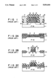
- An EPROM (electrically programmable read only memory) shown in FIG. 1, for example, is known as a conventional semiconductor memory device having a floating gate structure.
- the EPROM shown in FIG. 1 is manufactured by the steps shown in FIGS. 2A to 2C.
- first thermal oxide film 2 is formed on an island-like element region on p - -type silicon substrate 1 surrounded by field oxide film 1a.
- First polysilicon film 3, which will be formed into a floating gate electrode, is formed on the entire surface of second thermal oxide film 2 using the CVD (chemical vapor deposition) method. Thereafter, a phosphorous is doped into first polysilicon film 3. Then, the resultant structure is thermally oxidized at a low temperature of, e.g., 1,000° C. or below to form second thermal oxide film 4 on first polysilicon film 3.
- Second polysilicon film 5, which will be formed into a control gate electrode, is formed on the entire surface of second thermal oxide film 4 using the CVD method.
- a phosphorous is doped into second polysilicon film 5.
- photoresist film 6 having a predetermined pattern is formed on second polysilicon film 5.
- Films 5, 4, 3, and 2 are sequentially etched using photoresist film 6 as a mask to form first gate oxide film 12, floating gate electrode 13, second gate oxide film 14, and control gate electrode 15.
- An n-type impurity such as As ions is implanted in substrate 1 at a high concentration using this multilayer as a mask.
- the resultant structure is thermally oxidized to form thermal oxide film 7 on the entire surface of the multilayer and exposed portions of substrate 1, as shown in FIG.
- PSG film 10 serving as a passivation film is formed on the entire surface of the resultant structure.
- PSG film 10 and thermal oxide film 7 are selectively etched to form contact holes (not shown) leading to drain and source regions 8 and 9, respectively.
- an Al-Si film (not shown) is formed on the entire surface of the resultant structure.
- the Al-Si film is patterned to form source electrode 11 (FIG. 1) and drain electrode 12 (both of which are not shown in FIG. 2C, but are respectively denoted by reference numbers 11 and 12 in FIG. 1). With the above process, the EPROM cell shown in FIG. 1 is manufactured.
- control gate electrode 15 After writing of data, the electrons injected into floating gate electrode 13 are attracted by control gate electrode 15 through the second thermal oxide film, and hence escape from floating gate electrode 13. For this reason, the data may not be retained.
- First polysilicon film 3 serving as the floating gate electrode is composed of grains having various crystal orientations. For this reason, if first polysilicon film 3 is thermally oxidized at a low temperature of 1,000° C. or below to form second thermal oxide film 4 serving as second thermal oxide film 14, surface asperity appears at the interface between floating gate electrode 13 and second gate oxide film 14, resulting in a decrease in breakdown voltage of second thermal oxide film 14.
- Such a problem caused by low-temperature thermal oxidation can be eliminated by thermally oxidizing second thermal oxide film 4 at a high temperature of 1,100° C. or higher instead of at low temperature.
- a predetermined junction position may be changed, or a wafer may be warped. As a result, the performance of the semiconductor memory device is degraded, and the yield is decreased.
- the present invention has been made in consideration of the above situation, and has as its object to provide a semiconductor memory device, in which a second gate thermal oxide film can have a high breakdown voltage and an excellent memory retaining characteristic is obtained, and a method of manufacturing the same without decreasing the yield.
- a semiconductor memory device is characterized in that a floating gate electrode of a memory cell is composed of 2 to 10, preferably 2 to 5 silicon grains.
- a method of manufacturing a semiconductor memory device according to the present invention is characterized in that a first insulation film is formed on an element region of a semiconductor substrate, portions of the first insulation film on drain and source forming regions of the substrate are removed to expose the drain and source forming regions, and a polysilicon layer is formed on the entire surface of the structure in this state by the CVD method, so that 2 to 10, preferably 2 to 5 silicon grains are formed on a portion of the polysilicon layer, which serves as a floating gate electrode.
- the floating gate electrode is composed of a small number of grains. Therefore, even if the second insulation film is formed by low-temperature thermal oxidation, surface asperity at the interface of the second insulation film and the polysilicon layer composed of a small number of grains can be minimized. Hence, the breakdown voltage of the second insulation film can be increased. Especially, if the polysilicon layer is composed of 2 to 5 grains, the state of surface asperity becomes substantially equivalent to that of a single crystal, and hence is significantly reduced.
- the number of grains was measured by a transmission electron micrograph.
- a semiconductor memory device comprising:
- a semiconductor memory device having a floating gate structure comprising:
- a silicon substrate having a drain region and a source region
- a floating gate electrode formed of a polysilicon layer composed of 2 to 10 polysilicon grains
- control gate electrode formed of a polysilicon layer formed on said first insulation film
- a semiconductor memory device with a floating gate structure comprising:
- a silicon substrate having a drain region and a source region formed therein;
- a first polysilicon layer composed of 2 to 10 polysilicon grains, forming a floating gate electrode
- a method of manufacturing a semiconductor memory device comprising the steps of:
- silicon layer on said silicon substrate by an epitaxial growth process, said silicon layer having a portion which extends on said insulation film and composes 2 to 10 silicon grains;
- a method of manufacturing a semiconductor memory device having a floating gate structure comprising the steps of:
- a method of manufacturing a semiconductor memory device having a floating gate structure comprising the steps of:
- FIG. 1 is a sectional view of a conventional EPROM cell
- FIGS. 2A to 2C are sectional views of a structure of the conventional EPROM cell shown in FIG. 1 in each manufacturing step;
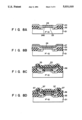
- FIG. 3 is a sectional view of an EPROM cell according to an embodiment of the present invention.
- FIGS. 4A to 4G are sectional views of a structure of the EPROM cell shown in FIG. 3 in each manufacturing step;
- FIG. 5 shows characteristic curves of the semiconductor memory device shown in FIGS. 3 and 4A to 4G;
- FIG. 6 is a sectional view of an EPROM according to another embodiment of the present invention.
- FIGS. 7A to 7D are sectional views of a structure of the EPROM cell shown in FIG. 6 in each manufacturing step.
- FIGS. 8A to 8D are sectional views of a structure of a modification of the EPROM cell shown in FIG. 6 in each manufacturing step.
- floating gate electrode 13 is formed of polysilicon, whereas in the embodiment shown in FIG. 3, floating gate electrode 30 is formed of 2 to 10 silicon grains. This is a characteristic feature of the present invention.
- FIG. 3 A method of manufacturing a memory device according to the embodiment (FIG. 3) will now be described with reference to FIGS. 4A to 4G.
- Field oxide film 22 having a thickness of about 1.2 ⁇ m is formed on p - -type silicon substrate 21 having a resistivity of about 10 to 20 ⁇ -cm using a normal selective oxidation technique (FIG. 4A).
- a first insulation film, i.e., first thermal oxide film 23 having a thickness of 500 ⁇ is formed on an island-like element region of substrate 21, surrounded by field oxide film 22. Then, a portion of film 23, on a drain forming region of substrate 21, is etched using NH 4 F gas to expose the drain forming region of substrate 21 (FIG. 4B).
- first polysilicon film 24 which is later formed into a floating gate electrode, is then formed on the entire surface of the resultant structure, using the CVD method.
- Film 24 is formed on the substrate at a substrate temperature of about 1,050° C. and a total SiH 2 Cl 2 pressure of 3.9 ⁇ 10 -3 Torr.
- the partial pressure of HCl is about 7 ⁇ 10 -3 Torr.
- the partial pressure of H 2 is about 2.0 ⁇ 10 -2 Torr.
- the number of grains in floating gate electrode portion 24a of first polysilicon film 24, grown from the exposed substrate region, i.e., the drain forming region would be 2 to 5 (FIG. 4C). The number of grains is measured by a transmission electron micrograph.
- Second polysilicon film 27 which is later formed into a control gate electrode, having a thickness of about 3,500 ⁇ and a sheet resistance of about 20 ⁇ , is formed on the entire surface of the resultant structure, using the CVD method. Thereafter, photoresist film 28 is formed on a portion of second polysilicon film 27, which corresponds to a channel region (FIG. 4D).
- second polysilicon film 27, second thermal oxide film 26, first polysilicon film 24, and first thermal oxide film 23 are sequentially etched using photoresist film 28 as a mask to form first gate thermal oxide film (gate insulation film) 29, floating gate electrode 30, second gate thermal oxide film 31, and control gate electrode 32.
- As ions were implanted in substrate 21 at an acceleration energy of about 60 KeV and at a dose of about 2.5 ⁇ 10 15 /cm 2 using this multilayer as a mask (FIG. 4E).
- photoresist film 28 is removed, and the resultant structure is thermally oxidized at a temperature of about 1,000° C. to form thermal oxide film 33 having a thickness of about 500 ⁇ on the entire surface.
- the implanted As ions are activated during the thermal oxidation to form n + -type drain and source regions 34 and 35, each having a sheet resistance of about 30 to 40 ⁇ and a depth of about 0.4 ⁇ m.
- PSG film 36 having a thickness of about 0.8 ⁇ m and serving as a passivation film, is formed on the entire surface of the resultant structure, using the CVD method (FIG. 4F).
- PSG film 36 and thermal oxide film 33 are selectively etched to form contact holes leading to drain and source regions 34 and 35, respectively.
- Al-Si film having a thickness of about 1.0 ⁇ m was formed on the entire surface of the resultant structure using the CVD method. Then, the Al-Si film is patterned to form drain and source electrodes 38 and 39 (FIG. 4G).
- the EPROM shown in FIG. 3 can be manufactured with the above process.
- first polysilicon film 24 is composed of a small number of grains and is formed in the step of FIG. 4C, even if the resultant structure is thermally oxidized at a low temperature of about 900° C. to form second thermal oxide film 26 on polysilicon film 24, the surface asperity at the interface of second thermal oxide film 26 and floating gate electrode portion 24a of first polysilicon film 24 is greatly reduced.
- second gate thermal oxide film 31 provides a high voltage. Therefore, even if a positive high voltage is accidentally applied to control gate electrode 32 of the EPROM shown in FIG. 4G, the electrons injected into floating gate portion 24 are not attracted by control gate electrode 32 and can not escape from floating gate portion 24, thereby retaining written data.
- second thermal oxide film 26 is formed by a low-temperature oxidation, substrate 21 is not warped. Therefore, the yield of semiconductor memory devices increases.
- FIG. 5 shows characteristic curves of the semiconductor memory device shown in FIGS. 3 and 4A to 4G.
- Characteristic curve I represents the relationship between the number of grains and the breakdown voltage (MV/cm).
- Characteristic curve II denotes the relationship between the number of grains and the yield of the device (%).
- the value of the number of grains is logarithmic. As shown in FIG. 5, when the number of grains is between 2 and 10, the breakdown voltage is higher than 5.8 (MV/cm) and the yield of the device is more than 50 (%). When the number of grains is more than 10, the breakdown voltage and the yield of the device are greatly reduced.
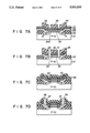
- FIG. 6 shows an EPROM according to another embodiment of the present invention.
- phosphorus-doped first polysilicon films 24 of a low resistance are left on drain and source regions 8 and 9.
- the surface area of each polysilicon film 24 thus left is larger than that of corresponding drain or source region 8 or 9, thereby increasing the masking margin for forming contact holes 37 for leading drain and source electrodes 38 and 39 to drain and source regions 8 and 9, respectively.
- the yield is improved.
- a method for manufacturing the EPROM shown in FIG. 6 will now be described with reference to FIGS. 7A to 7D. According to the method of this embodiment, after first thermal oxide film 23 was formed on the entire surface and before first polysilicon film 24 was formed, the portions of first thermal oxide film 23, which corresponded to drain and source regions 8 and 9, were removed.
- first thermal oxide film 22 and first thermal oxide film 23 were formed. Thereafter, portions of first thermal oxide film 23, on the forming regions of drain and source regions 8 and 9 of substrate 21, are removed, exposing the forming regions (FIG. 7A).
- First polysilicon layer 24 was formed on the entire surface of the resultant structure by the CVD method using a doping gas containing phosphorus.
- floating gate electrode portion 24a of first polysilicon layer 24, grown from the exposed substrate region (the drain and source forming regions) was a silicon layer composed of a small number of grains.
- n + -type drain and source regions 8 and 9 were respectively formed in the drain and source forming regions by phosphorus in the doping gas.
- second thermal oxide film 26 was formed on first polysilicon film 24, and second polysilicon film 27 was formed on the resultant structure.
- Photoresist film 28 having a predetermined pattern was formed on film 27.
- films 27, 26, 24, and 23 were selectively etched, using photoresist film 28 as a mask in the same manner as in the step of FIG. 4E, to form predetermined multilayers on drain and source regions 8 and 9, and a channel region.
- first polysilicon film 24 was divided into portions: a portion on drain region 8, a portion on source region 9, and a portion acting as floating gate electrode 24a.
- Photoresist film 28 was left on the portions of first polysilicon film 24 and second polysilicon film 27 on drain and source regions 8 and 9 so as to retain these portions (FIG. 7B).
- thermal oxide film 33 was formed on the entire surface.
- PSG film 36 was formed on the resultant structure (FIG. 7C).
- FIG. 8A the portions of second thermal oxide film 26, on the source and drain forming regions, were removed before second polysilicon film 27 was formed. Thereafter, as shown in FIG. 8B, second polysilicon film 27 was formed. In this case, thermal oxide film 33 and PSG film 36 were sequentially formed over the entire surface, as shown in FIG. 8C. Then, contact holes 37 were formed in first polysilicon film 27, as shown in FIG. 8D. Since it suffices that contact holes 37 were formed in second polysilicon film 27 in a shallow depth, the diameter of each contact hole 37 therefore decreased. As a result, the masking margin for forming contact holes 37, was further increased, as was the yield.
- the polysilicon films composed of a small number of grains were formed by the CVD method.
- the same effects as in the above embodiments can be anticipated when a floating gate electrode is composed of 10 grains or less by other methods.
- a first insulation film was formed, and then drain and source forming regions in a substrate were exposed.
- a polysilicon layer was formed on the entire surface by the CVD method.
- a floating gate electrode grown from the exposed substrate regions, was composed of a small number of grains.
- the breakdown voltage of a second insulation film formed on the floating gate electrode was significantly improved as compared with that of the second gate insulation film formed on the conventional polysilicon film. Therefore, the electrons that were injected into the floating gate electrode during the write operation, did not leak from the floating gate electrode, even when a high positive voltage was applied to the control gate electrode, and hence the device according to the present invention, exhibited excellent memory retaining characteristics.
- the second insulation film was formed on the silicon layer, composing a small number of grains. Therefore, even if it was formed by low-temperature oxidation, the second insulation film could have a sufficiently high breakdown voltage, and the yield of the semiconductor device would be increased.
Abstract
In a semiconductor memory device having a floating gate structure, the floating gate electrode is composed of 2 to 10 silicon grains. With the floating gate electrode, the insulation film, formed on the floating gate electrode, can have a high breakdown voltage. In a method of manufacturing a semiconductor memory device having a floating gate structure, an insulation film is formed on the silicon substrate, portions of the insulation film which are on the drain and source forming regions of the silicon substrate are removed, and a silicon layer is formed on the silicon substrate by an epitaxial growth process, constituting a floating gate, composed of 2 to 10 silicon grains. According to the manufacturing method, the insulation film formed on the floating gate electrode can have a high breakdown voltage.
Description
This application is a continuation of application Ser. No. 07/453,109 filed Dec. 22, 1989, now abandoned, which is a continuation of application Ser. No. 07/138,608 filed Dec. 29, 1987, now abandoned.
The present invention relates to a semiconductor memory device having a floating gate structure and a method of manufacturing the same.
An EPROM (electrically programmable read only memory) shown in FIG. 1, for example, is known as a conventional semiconductor memory device having a floating gate structure. The EPROM shown in FIG. 1 is manufactured by the steps shown in FIGS. 2A to 2C.
As shown in FIG. 2A, first thermal oxide film 2 is formed on an island-like element region on p- -type silicon substrate 1 surrounded by field oxide film 1a. First polysilicon film 3, which will be formed into a floating gate electrode, is formed on the entire surface of second thermal oxide film 2 using the CVD (chemical vapor deposition) method. Thereafter, a phosphorous is doped into first polysilicon film 3. Then, the resultant structure is thermally oxidized at a low temperature of, e.g., 1,000° C. or below to form second thermal oxide film 4 on first polysilicon film 3. Second polysilicon film 5, which will be formed into a control gate electrode, is formed on the entire surface of second thermal oxide film 4 using the CVD method. Then, a phosphorous is doped into second polysilicon film 5. Thereafter, as shown in FIG. 2B, photoresist film 6 having a predetermined pattern is formed on second polysilicon film 5. Films 5, 4, 3, and 2 are sequentially etched using photoresist film 6 as a mask to form first gate oxide film 12, floating gate electrode 13, second gate oxide film 14, and control gate electrode 15. An n-type impurity such as As ions is implanted in substrate 1 at a high concentration using this multilayer as a mask. Then, the resultant structure is thermally oxidized to form thermal oxide film 7 on the entire surface of the multilayer and exposed portions of substrate 1, as shown in FIG. 2C, while the implanted As ions are activated to form n+ -type drain and source regions 8 and 9. Thereafter, for example, PSG film 10 serving as a passivation film is formed on the entire surface of the resultant structure. PSG film 10 and thermal oxide film 7 are selectively etched to form contact holes (not shown) leading to drain and source regions 8 and 9, respectively. In addition, an Al-Si film (not shown) is formed on the entire surface of the resultant structure. The Al-Si film is patterned to form source electrode 11 (FIG. 1) and drain electrode 12 (both of which are not shown in FIG. 2C, but are respectively denoted by reference numbers 11 and 12 in FIG. 1). With the above process, the EPROM cell shown in FIG. 1 is manufactured.
In the above-described EPROM, electrons are injected into floating gate electrode 13 by applying a positive high voltage to n+ -type drain region 8 and control gate electrode 15, thereby writing data.
However, if a positive high voltage is applied for some reason to control gate electrode 15 after writing of data, the electrons injected into floating gate electrode 13 are attracted by control gate electrode 15 through the second thermal oxide film, and hence escape from floating gate electrode 13. For this reason, the data may not be retained.
Such an escape of electrons occurs because the breakdown voltage of second thermal oxide film 14 is low. The breakdown voltage is low for the following reason.
First polysilicon film 3 serving as the floating gate electrode is composed of grains having various crystal orientations. For this reason, if first polysilicon film 3 is thermally oxidized at a low temperature of 1,000° C. or below to form second thermal oxide film 4 serving as second thermal oxide film 14, surface asperity appears at the interface between floating gate electrode 13 and second gate oxide film 14, resulting in a decrease in breakdown voltage of second thermal oxide film 14. Such a problem caused by low-temperature thermal oxidation can be eliminated by thermally oxidizing second thermal oxide film 4 at a high temperature of 1,100° C. or higher instead of at low temperature. However, in high-temperature thermal oxidation, a predetermined junction position may be changed, or a wafer may be warped. As a result, the performance of the semiconductor memory device is degraded, and the yield is decreased.
The present invention has been made in consideration of the above situation, and has as its object to provide a semiconductor memory device, in which a second gate thermal oxide film can have a high breakdown voltage and an excellent memory retaining characteristic is obtained, and a method of manufacturing the same without decreasing the yield.
A semiconductor memory device according to the present invention is characterized in that a floating gate electrode of a memory cell is composed of 2 to 10, preferably 2 to 5 silicon grains. A method of manufacturing a semiconductor memory device according to the present invention is characterized in that a first insulation film is formed on an element region of a semiconductor substrate, portions of the first insulation film on drain and source forming regions of the substrate are removed to expose the drain and source forming regions, and a polysilicon layer is formed on the entire surface of the structure in this state by the CVD method, so that 2 to 10, preferably 2 to 5 silicon grains are formed on a portion of the polysilicon layer, which serves as a floating gate electrode.
According to the method described above, the floating gate electrode is composed of a small number of grains. Therefore, even if the second insulation film is formed by low-temperature thermal oxidation, surface asperity at the interface of the second insulation film and the polysilicon layer composed of a small number of grains can be minimized. Hence, the breakdown voltage of the second insulation film can be increased. Especially, if the polysilicon layer is composed of 2 to 5 grains, the state of surface asperity becomes substantially equivalent to that of a single crystal, and hence is significantly reduced.
In the present invention, the number of grains was measured by a transmission electron micrograph.
According to the present invention, there is provided a semiconductor memory device comprising:
a silicon substrate; and
a silicon layer constituting a floating gate electrode composed of 2 to 10 silicon grains.
According to the present invention, there is further provided a semiconductor memory device having a floating gate structure, comprising:
a silicon substrate having a drain region and a source region;
a floating gate electrode formed of a polysilicon layer composed of 2 to 10 polysilicon grains;
a first insulation film formed on said floating gate electrode;
a control gate electrode formed of a polysilicon layer formed on said first insulation film;
a second insulation film formed on the structure, and having contact holes leading to at least one of said drain region and source region; and
electrode layers extending in said contact holes formed in said second insulation film, and contacting said at least one of the drain region and source region.
According to the present invention, there is still further provided a semiconductor memory device with a floating gate structure, comprising:
a silicon substrate having a drain region and a source region formed therein;
a first polysilicon layer composed of 2 to 10 polysilicon grains, forming a floating gate electrode;
second polysilicon layers formed on at least one of said drain region and source region;
a first insulation film formed on said floating gate electrode;
a third polysilicon layer formed on said first insulation film, forming a control gate electrode;
fourth polysilicon layers formed on said second polysilicon layers;
a second insulation film formed on the structure, and having contact holes formed therein leading to said fourth polysilicon layers; and
electrode layers extending in said contact holes formed in said second insulation film, and contacting said second polysilicon layers.
According to the present invention, there is further provided a method of manufacturing a semiconductor memory device comprising the steps of:
forming an insulation film on a silicon substrate;
removing a predetermined portion of said insulation film;
forming a silicon layer on said silicon substrate by an epitaxial growth process, said silicon layer having a portion which extends on said insulation film and composes 2 to 10 silicon grains; and
removing a predetermined portion of said silicon layer to form a portion thereof which is separated from said substrate.
According to the present invention, there is still further provided a method of manufacturing a semiconductor memory device having a floating gate structure, comprising the steps of:
forming a first insulation film on a silicon substrate;
removing that portion of said insulation film, which is at least one of the drain and source forming regions of said silicon substrate to form a gate insulation film;
forming a first polysilicon layer composed of 2 to 10 silicon grains on said silicon substrate by an epitaxial growth process;
forming a second insulation film on said first polysilicon layer;
forming a second polysilicon layer on said second insulation film;
removing the predetermined portions of said first polysilicon layer, first insulation film, and second polysilicon layer, so that a portion thereof remains which is on said gate insulation film, and said at least one of the drain and source forming regions is exposed;
doping impurities into said drain and source forming regions to form a source and drain;
forming a third insulation film on the structure, having contact holes formed therein leading to at least one of said drain and source; and
forming electrodes extending in said contact holes formed in said third insulation film and contacting said at least one of the drain and source.
According to the present invention, there is yet further provided a method of manufacturing a semiconductor memory device having a floating gate structure, comprising the steps of:
forming a first insulation film on a silicon substrate;
removing that portion of said insulation film, which is on at least one of the drain and source forming regions of said silicon substrate to form a gate insulation film;
doping impurities into said drain and source forming regions to form a source and drain;
forming a first polysilicon layer composed of 2 to 10 silicon grains on said silicon substrate by an epitaxial growth process;
forming a second insulation film on said first polysilicon layer;
forming a second polysilicon layer on said second insulation film;
removing the predetermined portions of said first polysilicon layer, first insulation film, and second polysilicon layer, so that those portions thereof remain, which are on said gate insulation film and at least one of said drain and source;
forming a third insulation film on the structure;
forming contact holes in said third insulation film, second insulation film, and second polysilicon layer, leading to said portions of said second polysilicon layer remaining on said at least one of the source and drain; and
forming electrodes extending in said contact holes and contacting at least one of said portions of said second semiconductor layer remaining on said at least one of the source and drain.
FIG. 1 is a sectional view of a conventional EPROM cell;
FIGS. 2A to 2C are sectional views of a structure of the conventional EPROM cell shown in FIG. 1 in each manufacturing step;
FIG. 3 is a sectional view of an EPROM cell according to an embodiment of the present invention;
FIGS. 4A to 4G are sectional views of a structure of the EPROM cell shown in FIG. 3 in each manufacturing step;
FIG. 5 shows characteristic curves of the semiconductor memory device shown in FIGS. 3 and 4A to 4G;
FIG. 6 is a sectional view of an EPROM according to another embodiment of the present invention;
FIGS. 7A to 7D are sectional views of a structure of the EPROM cell shown in FIG. 6 in each manufacturing step; and
FIGS. 8A to 8D are sectional views of a structure of a modification of the EPROM cell shown in FIG. 6 in each manufacturing step.
An EPROM according to an embodiment of the present invention will be described below with reference to the accompanying drawings.
The same reference numerals in FIG. 3 denote the same parts as in FIG. 1. In the conventional device shown in FIG. 1, floating gate electrode 13 is formed of polysilicon, whereas in the embodiment shown in FIG. 3, floating gate electrode 30 is formed of 2 to 10 silicon grains. This is a characteristic feature of the present invention.
A method of manufacturing a memory device according to the embodiment (FIG. 3) will now be described with reference to FIGS. 4A to 4G.
Field oxide film 22 having a thickness of about 1.2 μm is formed on p- -type silicon substrate 21 having a resistivity of about 10 to 20 Ω-cm using a normal selective oxidation technique (FIG. 4A). A first insulation film, i.e., first thermal oxide film 23 having a thickness of 500 Å is formed on an island-like element region of substrate 21, surrounded by field oxide film 22. Then, a portion of film 23, on a drain forming region of substrate 21, is etched using NH4 F gas to expose the drain forming region of substrate 21 (FIG. 4B).
Subsequently, 1,000-Å thick first polysilicon film 24, which is later formed into a floating gate electrode, is then formed on the entire surface of the resultant structure, using the CVD method. Film 24 is formed on the substrate at a substrate temperature of about 1,050° C. and a total SiH2 Cl2 pressure of 3.9 × 10⁻³ Torr. The partial pressure of HCl is about 7 × 10⁻³ Torr. and the partial pressure of H2 is about 2.0 × 10⁻² Torr. In this case, the number of grains in floating gate electrode portion 24a of first polysilicon film 24, grown from the exposed substrate region, i.e., the drain forming region, would be 2 to 5 (FIG. 4C). The number of grains is measured by a transmission electron micrograph.
Subsequently, phosphorus is doped into first polysilicon film 24 by thermal diffusion. The resultant structure is thermally oxidized at a temperature of 900° C. to form 500-Å thick second thermal oxide film 26 on first polysilicon film 24. Second polysilicon film 27, which is later formed into a control gate electrode, having a thickness of about 3,500 Å and a sheet resistance of about 20 Ω, is formed on the entire surface of the resultant structure, using the CVD method. Thereafter, photoresist film 28 is formed on a portion of second polysilicon film 27, which corresponds to a channel region (FIG. 4D).
Then, second polysilicon film 27, second thermal oxide film 26, first polysilicon film 24, and first thermal oxide film 23 are sequentially etched using photoresist film 28 as a mask to form first gate thermal oxide film (gate insulation film) 29, floating gate electrode 30, second gate thermal oxide film 31, and control gate electrode 32. Following this, As ions were implanted in substrate 21 at an acceleration energy of about 60 KeV and at a dose of about 2.5 × 10¹⁵ /cm2 using this multilayer as a mask (FIG. 4E).
Thereafter, photoresist film 28 is removed, and the resultant structure is thermally oxidized at a temperature of about 1,000° C. to form thermal oxide film 33 having a thickness of about 500 Å on the entire surface. The implanted As ions are activated during the thermal oxidation to form n+ -type drain and source regions 34 and 35, each having a sheet resistance of about 30 to 40 Ω and a depth of about 0.4 μm. Then, PSG film 36 having a thickness of about 0.8 μm and serving as a passivation film, is formed on the entire surface of the resultant structure, using the CVD method (FIG. 4F).
Subsequently, PSG film 36 and thermal oxide film 33 are selectively etched to form contact holes leading to drain and source regions 34 and 35, respectively. Al-Si film having a thickness of about 1.0 μm was formed on the entire surface of the resultant structure using the CVD method. Then, the Al-Si film is patterned to form drain and source electrodes 38 and 39 (FIG. 4G). The EPROM shown in FIG. 3 can be manufactured with the above process.
According to the manufacturing method of the embodiment, since first polysilicon film 24 is composed of a small number of grains and is formed in the step of FIG. 4C, even if the resultant structure is thermally oxidized at a low temperature of about 900° C. to form second thermal oxide film 26 on polysilicon film 24, the surface asperity at the interface of second thermal oxide film 26 and floating gate electrode portion 24a of first polysilicon film 24 is greatly reduced. As a result, second gate thermal oxide film 31 provides a high voltage. Therefore, even if a positive high voltage is accidentally applied to control gate electrode 32 of the EPROM shown in FIG. 4G, the electrons injected into floating gate portion 24 are not attracted by control gate electrode 32 and can not escape from floating gate portion 24, thereby retaining written data.
According to the above method, because second thermal oxide film 26 is formed by a low-temperature oxidation, substrate 21 is not warped. Therefore, the yield of semiconductor memory devices increases.
FIG. 5 shows characteristic curves of the semiconductor memory device shown in FIGS. 3 and 4A to 4G. Characteristic curve I represents the relationship between the number of grains and the breakdown voltage (MV/cm). Characteristic curve II denotes the relationship between the number of grains and the yield of the device (%). In FIG. 5, the value of the number of grains is logarithmic. As shown in FIG. 5, when the number of grains is between 2 and 10, the breakdown voltage is higher than 5.8 (MV/cm) and the yield of the device is more than 50 (%). When the number of grains is more than 10, the breakdown voltage and the yield of the device are greatly reduced.
FIG. 6 shows an EPROM according to another embodiment of the present invention. In this embodiment, phosphorus-doped first polysilicon films 24 of a low resistance are left on drain and source regions 8 and 9. The surface area of each polysilicon film 24 thus left is larger than that of corresponding drain or source region 8 or 9, thereby increasing the masking margin for forming contact holes 37 for leading drain and source electrodes 38 and 39 to drain and source regions 8 and 9, respectively. As a result, the yield is improved.
A method for manufacturing the EPROM shown in FIG. 6 will now be described with reference to FIGS. 7A to 7D. According to the method of this embodiment, after first thermal oxide film 23 was formed on the entire surface and before first polysilicon film 24 was formed, the portions of first thermal oxide film 23, which corresponded to drain and source regions 8 and 9, were removed.
The same contents as described with reference to FIGS. 4A and 4G will now be simply explained by referring to the same figures.
As is shown in FIGS. 4A and 4B, field oxide film 22 and first thermal oxide film 23 were formed. Thereafter, portions of first thermal oxide film 23, on the forming regions of drain and source regions 8 and 9 of substrate 21, are removed, exposing the forming regions (FIG. 7A). First polysilicon layer 24 was formed on the entire surface of the resultant structure by the CVD method using a doping gas containing phosphorus. In this case, floating gate electrode portion 24a of first polysilicon layer 24, grown from the exposed substrate region (the drain and source forming regions), was a silicon layer composed of a small number of grains. When first polysilicon layer 24 was grown, n+ -type drain and source regions 8 and 9 were respectively formed in the drain and source forming regions by phosphorus in the doping gas.
Next the same step as shown in FIG. 4D was performed. More specifically, second thermal oxide film 26 was formed on first polysilicon film 24, and second polysilicon film 27 was formed on the resultant structure. Photoresist film 28 having a predetermined pattern was formed on film 27. Then, films 27, 26, 24, and 23 were selectively etched, using photoresist film 28 as a mask in the same manner as in the step of FIG. 4E, to form predetermined multilayers on drain and source regions 8 and 9, and a channel region. Upon etching, first polysilicon film 24 was divided into portions: a portion on drain region 8, a portion on source region 9, and a portion acting as floating gate electrode 24a. Photoresist film 28 was left on the portions of first polysilicon film 24 and second polysilicon film 27 on drain and source regions 8 and 9 so as to retain these portions (FIG. 7B).
Subsequently, thermal oxide film 33 was formed on the entire surface. PSG film 36 was formed on the resultant structure (FIG. 7C). Contact holes 37, leading to drain and source regions 8 and 9, were formed in the same manner as in the step of FIG. 4G. Drain and source electrodes 38 and 39 were formed in contact holes 37, thereby completing the memory cell shown in FIG. 6 (FIG. 7D).
As shown in FIG. 8A, the portions of second thermal oxide film 26, on the source and drain forming regions, were removed before second polysilicon film 27 was formed. Thereafter, as shown in FIG. 8B, second polysilicon film 27 was formed. In this case, thermal oxide film 33 and PSG film 36 were sequentially formed over the entire surface, as shown in FIG. 8C. Then, contact holes 37 were formed in first polysilicon film 27, as shown in FIG. 8D. Since it suffices that contact holes 37 were formed in second polysilicon film 27 in a shallow depth, the diameter of each contact hole 37 therefore decreased. As a result, the masking margin for forming contact holes 37, was further increased, as was the yield.
In the embodiments shown in FIGS. 6, 7A to 7D and 8A to 8D, the characteristic curves are substantially the same as those of which were obtained in FIG. 5.
Note that even if the manufacturing methods, described with reference to FIGS. 7A to 7D, and 8A to 8D, are applied to the formation of only one of the source and drain, the masking margin for forming a contact hole is increased.
In the first and second embodiments, the polysilicon films composed of a small number of grains were formed by the CVD method. However, the same effects as in the above embodiments can be anticipated when a floating gate electrode is composed of 10 grains or less by other methods.
According to the present invention, a first insulation film was formed, and then drain and source forming regions in a substrate were exposed. In this state, a polysilicon layer was formed on the entire surface by the CVD method. In this case, a floating gate electrode, grown from the exposed substrate regions, was composed of a small number of grains. As a result, the breakdown voltage of a second insulation film formed on the floating gate electrode, composed of a small number of grains, was significantly improved as compared with that of the second gate insulation film formed on the conventional polysilicon film. Therefore, the electrons that were injected into the floating gate electrode during the write operation, did not leak from the floating gate electrode, even when a high positive voltage was applied to the control gate electrode, and hence the device according to the present invention, exhibited excellent memory retaining characteristics. In addition, the second insulation film was formed on the silicon layer, composing a small number of grains. Therefore, even if it was formed by low-temperature oxidation, the second insulation film could have a sufficiently high breakdown voltage, and the yield of the semiconductor device would be increased.
Claims (4)
1. A nonvolatile semiconductor memory device with a floating gate structure, comprising:
a silicon substrate;
a floating gate electrode composed of 2 to 10 silicon grains for limiting a number of asperities therein, said floating gate electrode having a potential; and
a control electrode for controlling the potential of said floating gate electrode.
2. A nonvolatile semiconductor memory device having a floating gate structure, comprising:
a silicon substrate having a drain region and a source region;
a floating gate electrode composed of 2 to 10 polysilicon grains for limiting a number of asperities therein, said floating gate electrode having a potential;
a first insulation film formed on said floating gate electrode;
a control gate electrode comprising a polysilicon layer formed on said first insulation film, for controlling the potential of said floating gate electrode;
a second insulation film formed on the structure, and having contact holes leading to at least one of said drain region and source region; and
electrode layers extending in said contact holes formed in said second insulation film, and contacting at least one of said drain region and source region.
3. A nonvolatile semiconductor memory device with a floating gate structure, comprising:
a silicon substrate having a drain region and a source region formed therein;
a first polysilicon layer a having floating gate electrode composed of 2 to 10 polysilicon grains for limiting a number of asperities therein, said floating gate electrode having a potential;
second polysilicon layers formed on at least one of said drain region and source region;
a first insulation film formed on said floating gate electrode;
a third polysilicon layer formed on said first insulation film, forming a control gate electrode for controlling the potential of said floating gate electrode;
fourth polysilicon layers formed on said second polysilicon layers;
a second insulation film formed on the structure, and having contact holes formed therein leading to said fourth polysilicon layers; and
electrode layers extending in said contact holes formed in said second insulation film, and contacting said second polysilicon layers.
4. A semiconductor memory device according to claim 3, wherein said fourth polysilicon layers comprise contact holes formed therein and continuous to said contact holes formed in said second insulation film, and wherein said semiconductor memory device further comprises third insulation films formed between said second polysilicon layers and said fourth polysilicon layers, said third insulation films having contact holes formed therein and continuous to said contact holes formed in said fourth polysilicon layers and said second insulation film.
Priority Applications (1)
| Application Number | Priority Date | Filing Date | Title |
|---|---|---|---|
| US07/684,870 US5149666A (en) | 1987-01-07 | 1991-04-15 | Method of manufacturing a semiconductor memory device having a floating gate electrode composed of 2-10 silicon grains |
Applications Claiming Priority (2)
| Application Number | Priority Date | Filing Date | Title |
|---|---|---|---|
| JP62-593 | 1987-01-07 | ||
| JP62000593A JP2633541B2 (en) | 1987-01-07 | 1987-01-07 | Method for manufacturing semiconductor memory device |
Related Parent Applications (1)
| Application Number | Title | Priority Date | Filing Date |
|---|---|---|---|
| US45310989A Continuation | 1987-01-07 | 1989-12-22 |
Related Child Applications (1)
| Application Number | Title | Priority Date | Filing Date |
|---|---|---|---|
| US07/684,870 Division US5149666A (en) | 1987-01-07 | 1991-04-15 | Method of manufacturing a semiconductor memory device having a floating gate electrode composed of 2-10 silicon grains |
Publications (1)
| Publication Number | Publication Date |
|---|---|
| US5031010A true US5031010A (en) | 1991-07-09 |
Family
ID=11478035
Family Applications (1)
| Application Number | Title | Priority Date | Filing Date |
|---|---|---|---|
| US07/622,148 Expired - Fee Related US5031010A (en) | 1987-01-07 | 1990-12-03 | Semiconductor memory device and method of manufacturing the same |
Country Status (5)
| Country | Link |
|---|---|
| US (1) | US5031010A (en) |
| EP (1) | EP0274390B1 (en) |
| JP (1) | JP2633541B2 (en) |
| KR (1) | KR910003098B1 (en) |
| DE (1) | DE3879719T2 (en) |
Cited By (4)
| Publication number | Priority date | Publication date | Assignee | Title |
|---|---|---|---|---|
| US5357134A (en) * | 1991-10-31 | 1994-10-18 | Rohm Co., Ltd. | Nonvolatile semiconductor device having charge trap film containing silicon crystal grains |
| US5913111A (en) * | 1995-01-18 | 1999-06-15 | Canon Kabushiki Kaisha | Method of manufacturing an insulaed gate transistor |
| US6465840B1 (en) * | 1997-05-08 | 2002-10-15 | Sgs-Thomson Microelectronics S.R.L. | Integrated structure comprising a patterned feature substantially of single grain polysilicon |
| US20030096462A1 (en) * | 2000-06-23 | 2003-05-22 | Hiroshi Tanabe | Thin-film transistor and method of manufacture thereof |
Families Citing this family (3)
| Publication number | Priority date | Publication date | Assignee | Title |
|---|---|---|---|---|
| US5106772A (en) * | 1990-01-09 | 1992-04-21 | Intel Corporation | Method for improving the electrical erase characteristics of floating gate memory cells by immediately depositing a protective polysilicon layer following growth of the tunnel or gate oxide |
| US7588982B2 (en) * | 2006-08-29 | 2009-09-15 | Micron Technology, Inc. | Methods of forming semiconductor constructions and flash memory cells |
| EP2495762B1 (en) | 2011-03-03 | 2017-11-01 | IMEC vzw | Method for producing a floating gate semiconductor memory device |
Citations (13)
| Publication number | Priority date | Publication date | Assignee | Title |
|---|---|---|---|---|
| JPS5118782A (en) * | 1974-08-06 | 1976-02-14 | Toa Nenryo Kogyo Kk | Atakuchitsuku horipuropirenno datsukaiseiseiho |
| US4203158A (en) * | 1978-02-24 | 1980-05-13 | Intel Corporation | Electrically programmable and erasable MOS floating gate memory device employing tunneling and method of fabricating same |
| US4396933A (en) * | 1971-06-18 | 1983-08-02 | International Business Machines Corporation | Dielectrically isolated semiconductor devices |
| US4458407A (en) * | 1983-04-01 | 1984-07-10 | International Business Machines Corporation | Process for fabricating semi-conductive oxide between two poly silicon gate electrodes |
| JPS59125665A (en) * | 1983-01-06 | 1984-07-20 | Toshiba Corp | Manufacture of semiconductor memory device |
| EP0164605A2 (en) * | 1984-05-17 | 1985-12-18 | Kabushiki Kaisha Toshiba | Method of manufacturing nonvolatile semiconductor EEPROM device |
| US4584205A (en) * | 1984-07-02 | 1986-04-22 | Signetics Corporation | Method for growing an oxide layer on a silicon surface |
| US4669062A (en) * | 1984-09-21 | 1987-05-26 | Fujitsu Limited | Two-tiered dynamic random access memory (DRAM) cell |
| US4680609A (en) * | 1984-09-24 | 1987-07-14 | Northern Telecom Limited | Structure and fabrication of vertically integrated CMOS logic gates |
| US4812898A (en) * | 1985-06-21 | 1989-03-14 | Nec Corporation | Electronically programmable and erasable memory device having floating gate electrode with a unique distribution of impurity concentration |
| US4868629A (en) * | 1984-05-15 | 1989-09-19 | Waferscale Integration, Inc. | Self-aligned split gate EPROM |
| US4874716A (en) * | 1986-04-01 | 1989-10-17 | Texas Instrument Incorporated | Process for fabricating integrated circuit structure with extremely smooth polysilicone dielectric interface |
| US4931847A (en) * | 1986-06-27 | 1990-06-05 | Sgs-Thomson Microelectronics S.P.A. | Floating gate memory with sidewall tunnelling area |
Family Cites Families (1)
| Publication number | Priority date | Publication date | Assignee | Title |
|---|---|---|---|---|
| JPS5931231B2 (en) * | 1980-01-31 | 1984-07-31 | 工業技術院長 | Floating gate non-volatile semiconductor memory |
-
1987
- 1987-01-07 JP JP62000593A patent/JP2633541B2/en not_active Expired - Lifetime
- 1987-12-30 KR KR1019870015382A patent/KR910003098B1/en not_active IP Right Cessation
-
1988
- 1988-01-07 EP EP88100116A patent/EP0274390B1/en not_active Expired - Lifetime
- 1988-01-07 DE DE88100116T patent/DE3879719T2/en not_active Expired - Fee Related
-
1990
- 1990-12-03 US US07/622,148 patent/US5031010A/en not_active Expired - Fee Related
Patent Citations (14)
| Publication number | Priority date | Publication date | Assignee | Title |
|---|---|---|---|---|
| US4396933A (en) * | 1971-06-18 | 1983-08-02 | International Business Machines Corporation | Dielectrically isolated semiconductor devices |
| JPS5118782A (en) * | 1974-08-06 | 1976-02-14 | Toa Nenryo Kogyo Kk | Atakuchitsuku horipuropirenno datsukaiseiseiho |
| US4203158A (en) * | 1978-02-24 | 1980-05-13 | Intel Corporation | Electrically programmable and erasable MOS floating gate memory device employing tunneling and method of fabricating same |
| US4203158B1 (en) * | 1978-02-24 | 1992-09-22 | Intel Corp | |
| JPS59125665A (en) * | 1983-01-06 | 1984-07-20 | Toshiba Corp | Manufacture of semiconductor memory device |
| US4458407A (en) * | 1983-04-01 | 1984-07-10 | International Business Machines Corporation | Process for fabricating semi-conductive oxide between two poly silicon gate electrodes |
| US4868629A (en) * | 1984-05-15 | 1989-09-19 | Waferscale Integration, Inc. | Self-aligned split gate EPROM |
| EP0164605A2 (en) * | 1984-05-17 | 1985-12-18 | Kabushiki Kaisha Toshiba | Method of manufacturing nonvolatile semiconductor EEPROM device |
| US4584205A (en) * | 1984-07-02 | 1986-04-22 | Signetics Corporation | Method for growing an oxide layer on a silicon surface |
| US4669062A (en) * | 1984-09-21 | 1987-05-26 | Fujitsu Limited | Two-tiered dynamic random access memory (DRAM) cell |
| US4680609A (en) * | 1984-09-24 | 1987-07-14 | Northern Telecom Limited | Structure and fabrication of vertically integrated CMOS logic gates |
| US4812898A (en) * | 1985-06-21 | 1989-03-14 | Nec Corporation | Electronically programmable and erasable memory device having floating gate electrode with a unique distribution of impurity concentration |
| US4874716A (en) * | 1986-04-01 | 1989-10-17 | Texas Instrument Incorporated | Process for fabricating integrated circuit structure with extremely smooth polysilicone dielectric interface |
| US4931847A (en) * | 1986-06-27 | 1990-06-05 | Sgs-Thomson Microelectronics S.P.A. | Floating gate memory with sidewall tunnelling area |
Non-Patent Citations (4)
| Title |
|---|
| J. Collinge et al., "Field-Effect in Large Grain Polysilicon Transistors," IEEE IEDM Conf. Proc. (1982), pp. 444-447. |
| J. Collinge et al., Field Effect in Large Grain Polysilicon Transistors, IEEE IEDM Conf. Proc. (1982), pp. 444 447. * |
| R. M. Anderson et al., "Evidence for Surface asperity mechanism of conductivity in oxide grown on polycrystalline silicon", Journal of Applied Physics, vol. 48 (Sep. 1977) pp. 4834-4836. |
| R. M. Anderson et al., Evidence for Surface asperity mechanism of conductivity in oxide grown on polycrystalline silicon , Journal of Applied Physics, vol. 48 (Sep. 1977) pp. 4834 4836. * |
Cited By (6)
| Publication number | Priority date | Publication date | Assignee | Title |
|---|---|---|---|---|
| US5357134A (en) * | 1991-10-31 | 1994-10-18 | Rohm Co., Ltd. | Nonvolatile semiconductor device having charge trap film containing silicon crystal grains |
| US5913111A (en) * | 1995-01-18 | 1999-06-15 | Canon Kabushiki Kaisha | Method of manufacturing an insulaed gate transistor |
| US6465840B1 (en) * | 1997-05-08 | 2002-10-15 | Sgs-Thomson Microelectronics S.R.L. | Integrated structure comprising a patterned feature substantially of single grain polysilicon |
| US6746940B2 (en) | 1997-05-08 | 2004-06-08 | Sgs-Thomson Microeletronics S.R.L. | Integrated structure comprising a patterned feature substantially of single grain polysilicon |
| US20030096462A1 (en) * | 2000-06-23 | 2003-05-22 | Hiroshi Tanabe | Thin-film transistor and method of manufacture thereof |
| US7052944B2 (en) * | 2000-06-23 | 2006-05-30 | Nec Corporation | Thin-film transistor and method of manufacture thereof |
Also Published As
| Publication number | Publication date |
|---|---|
| JPS63169069A (en) | 1988-07-13 |
| JP2633541B2 (en) | 1997-07-23 |
| EP0274390A3 (en) | 1989-03-29 |
| DE3879719T2 (en) | 1993-10-07 |
| EP0274390A2 (en) | 1988-07-13 |
| DE3879719D1 (en) | 1993-05-06 |
| KR910003098B1 (en) | 1991-05-18 |
| EP0274390B1 (en) | 1993-03-31 |
| KR880009426A (en) | 1988-09-15 |
Similar Documents
| Publication | Publication Date | Title |
|---|---|---|
| JP3911043B2 (en) | Nonvolatile memory device and manufacturing method thereof | |
| US6303440B1 (en) | Nonvolatile semiconductor memory, and method of manufacturing the same | |
| KR100217274B1 (en) | Process of fabricating semiconductor device | |
| US5106774A (en) | Method of making trench type dynamic random access memory device | |
| US5031010A (en) | Semiconductor memory device and method of manufacturing the same | |
| US5149666A (en) | Method of manufacturing a semiconductor memory device having a floating gate electrode composed of 2-10 silicon grains | |
| US5237196A (en) | Semiconductor device and method for manufacturing the same | |
| JPH07147329A (en) | Semiconductor device | |
| EP0287031B1 (en) | High breakdown voltage insulating film provided between polysilicon layers | |
| EP0383011B1 (en) | Semiconductor non-volatile memory device | |
| JP2870086B2 (en) | Manufacturing method of MOS nonvolatile semiconductor memory device | |
| JPH07161835A (en) | Manufacture of semiconductor memory device | |
| JP2833389B2 (en) | Manufacturing method of nonvolatile semiconductor memory device | |
| JP2829012B2 (en) | Semiconductor nonvolatile memory device and method of manufacturing the same | |
| JP3371196B2 (en) | Pattern formation method | |
| JP3397804B2 (en) | Manufacturing method of nonvolatile memory | |
| JP2674112B2 (en) | Method for manufacturing semiconductor device | |
| JP3054614B2 (en) | Semiconductor device | |
| JP3078109B2 (en) | Method for manufacturing semiconductor device | |
| JP3138538B2 (en) | Semiconductor nonvolatile memory element and method of manufacturing the same | |
| JPH0381297B2 (en) | ||
| JP3492718B2 (en) | Method for manufacturing semiconductor memory device | |
| JPH01260857A (en) | Semiconductor device and manufacture thereof | |
| JP3257070B2 (en) | Semiconductor storage device | |
| JPH06318710A (en) | Nonvolatile semiconductor storage device and its manufacture |
Legal Events
| Date | Code | Title | Description |
|---|---|---|---|
| FEPP | Fee payment procedure |
Free format text: PAYOR NUMBER ASSIGNED (ORIGINAL EVENT CODE: ASPN); ENTITY STATUS OF PATENT OWNER: LARGE ENTITY |
|
| FPAY | Fee payment |
Year of fee payment: 4 |
|
| FPAY | Fee payment |
Year of fee payment: 8 |
|
| REMI | Maintenance fee reminder mailed | ||
| LAPS | Lapse for failure to pay maintenance fees | ||
| STCH | Information on status: patent discontinuation |
Free format text: PATENT EXPIRED DUE TO NONPAYMENT OF MAINTENANCE FEES UNDER 37 CFR 1.362 |
|
| FP | Lapsed due to failure to pay maintenance fee |
Effective date: 20030709 |