US5051802A - Compact image sensor - Google Patents
Compact image sensor Download PDFInfo
- Publication number
- US5051802A US5051802A US07/563,826 US56382690A US5051802A US 5051802 A US5051802 A US 5051802A US 56382690 A US56382690 A US 56382690A US 5051802 A US5051802 A US 5051802A
- Authority
- US
- United States
- Prior art keywords
- package
- window
- photosensitive elements
- terminals
- contacts
- Prior art date
- Legal status (The legal status is an assumption and is not a legal conclusion. Google has not performed a legal analysis and makes no representation as to the accuracy of the status listed.)
- Expired - Lifetime
Links
- 239000000758 substrate Substances 0.000 claims abstract description 24
- 125000006850 spacer group Chemical group 0.000 claims description 13
- 239000004020 conductor Substances 0.000 claims description 8
- 239000012777 electrically insulating material Substances 0.000 claims description 7
- 229910052738 indium Inorganic materials 0.000 claims description 3
- APFVFJFRJDLVQX-UHFFFAOYSA-N indium atom Chemical compound [In] APFVFJFRJDLVQX-UHFFFAOYSA-N 0.000 claims description 3
- 239000002184 metal Substances 0.000 claims description 2
- 229910052751 metal Inorganic materials 0.000 claims description 2
- 239000004065 semiconductor Substances 0.000 claims 7
- 230000005855 radiation Effects 0.000 claims 2
- 239000000463 material Substances 0.000 description 6
- 210000000056 organ Anatomy 0.000 description 5
- RYGMFSIKBFXOCR-UHFFFAOYSA-N Copper Chemical compound [Cu] RYGMFSIKBFXOCR-UHFFFAOYSA-N 0.000 description 3
- 229910052802 copper Inorganic materials 0.000 description 3
- 239000010949 copper Substances 0.000 description 3
- 229920003023 plastic Polymers 0.000 description 3
- 239000000919 ceramic Substances 0.000 description 2
- 238000001839 endoscopy Methods 0.000 description 2
- 239000011521 glass Substances 0.000 description 2
- 239000011159 matrix material Substances 0.000 description 2
- 239000004033 plastic Substances 0.000 description 2
- 229910052710 silicon Inorganic materials 0.000 description 2
- 239000010703 silicon Substances 0.000 description 2
- 229920001971 elastomer Polymers 0.000 description 1
- 239000000806 elastomer Substances 0.000 description 1
- 239000003822 epoxy resin Substances 0.000 description 1
- 239000002991 molded plastic Substances 0.000 description 1
- 229920000647 polyepoxide Polymers 0.000 description 1
- 230000035945 sensitivity Effects 0.000 description 1
- 229910052709 silver Inorganic materials 0.000 description 1
- 239000004332 silver Substances 0.000 description 1
- 239000012780 transparent material Substances 0.000 description 1
Images

Classifications
-
- H—ELECTRICITY
- H01—ELECTRIC ELEMENTS
- H01L—SEMICONDUCTOR DEVICES NOT COVERED BY CLASS H10
- H01L31/00—Semiconductor devices sensitive to infrared radiation, light, electromagnetic radiation of shorter wavelength or corpuscular radiation and specially adapted either for the conversion of the energy of such radiation into electrical energy or for the control of electrical energy by such radiation; Processes or apparatus specially adapted for the manufacture or treatment thereof or of parts thereof; Details thereof
- H01L31/02—Details
- H01L31/0203—Containers; Encapsulations, e.g. encapsulation of photodiodes
-
- H—ELECTRICITY
- H01—ELECTRIC ELEMENTS
- H01L—SEMICONDUCTOR DEVICES NOT COVERED BY CLASS H10
- H01L27/00—Devices consisting of a plurality of semiconductor or other solid-state components formed in or on a common substrate
- H01L27/14—Devices consisting of a plurality of semiconductor or other solid-state components formed in or on a common substrate including semiconductor components sensitive to infrared radiation, light, electromagnetic radiation of shorter wavelength or corpuscular radiation and specially adapted either for the conversion of the energy of such radiation into electrical energy or for the control of electrical energy by such radiation
- H01L27/144—Devices controlled by radiation
- H01L27/146—Imager structures
- H01L27/14601—Structural or functional details thereof
- H01L27/14618—Containers
-
- H—ELECTRICITY
- H01—ELECTRIC ELEMENTS
- H01L—SEMICONDUCTOR DEVICES NOT COVERED BY CLASS H10
- H01L31/00—Semiconductor devices sensitive to infrared radiation, light, electromagnetic radiation of shorter wavelength or corpuscular radiation and specially adapted either for the conversion of the energy of such radiation into electrical energy or for the control of electrical energy by such radiation; Processes or apparatus specially adapted for the manufacture or treatment thereof or of parts thereof; Details thereof
- H01L31/02—Details
- H01L31/02002—Arrangements for conducting electric current to or from the device in operations
- H01L31/02005—Arrangements for conducting electric current to or from the device in operations for device characterised by at least one potential jump barrier or surface barrier
-
- H—ELECTRICITY
- H01—ELECTRIC ELEMENTS
- H01L—SEMICONDUCTOR DEVICES NOT COVERED BY CLASS H10
- H01L2224/00—Indexing scheme for arrangements for connecting or disconnecting semiconductor or solid-state bodies and methods related thereto as covered by H01L24/00
- H01L2224/01—Means for bonding being attached to, or being formed on, the surface to be connected, e.g. chip-to-package, die-attach, "first-level" interconnects; Manufacturing methods related thereto
- H01L2224/42—Wire connectors; Manufacturing methods related thereto
- H01L2224/47—Structure, shape, material or disposition of the wire connectors after the connecting process
- H01L2224/48—Structure, shape, material or disposition of the wire connectors after the connecting process of an individual wire connector
- H01L2224/484—Connecting portions
- H01L2224/4847—Connecting portions the connecting portion on the bonding area of the semiconductor or solid-state body being a wedge bond
- H01L2224/48472—Connecting portions the connecting portion on the bonding area of the semiconductor or solid-state body being a wedge bond the other connecting portion not on the bonding area also being a wedge bond, i.e. wedge-to-wedge
-
- H—ELECTRICITY
- H01—ELECTRIC ELEMENTS
- H01L—SEMICONDUCTOR DEVICES NOT COVERED BY CLASS H10
- H01L2924/00—Indexing scheme for arrangements or methods for connecting or disconnecting semiconductor or solid-state bodies as covered by H01L24/00
- H01L2924/01—Chemical elements
- H01L2924/01014—Silicon [Si]
Definitions
- the present invention concerns a compact image sensor.
- This sensor can be applied notably in endoscopy. In this application, it is clearly necessary for the sensor to occupy as little space as possible while, at the same time, preserving acceptable electro-optical performance characteristics with regard to photosensitive surface, resolution, sensitivity, etc.
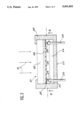
- FIGS. 1 and 2 give a schematic view of a compact image sensor of the prior art.
- FIG. 1 shows a schematic cross-section of this sensor and
- FIG. 2 shows a schematic section along AA of the sensor of FIG. 1.
- the same references are repeated for the same elements in FIGS. 1 and 2.
- This sensor has an imperviously sealed package 1, made of an electrically insulating material, for example a molded plastic material.
- This package has a front face 2, with a window 3, made of an electrically insulating material, which is transparent to light rays R coming from a part of an organ of the human body or from an object for which it is sought to obtain an image.
- the material forming the window 3 is made, for example, of glass or of a transparent plastic material. It is clear that when this sensor is used to obtain images of the inside of a human organ, the inside of this organ is illuminated by a light source which is independent of the sensor.
- This sensor also has a rear face 4, forming the back of the package 1. This rear face is parallel to the front face.
- the inside of the package contains a stack arrangement comprising an insulating support 5, formed, for example, by a ceramic, and a set 6 of photosensitive elements on a semiconducting substrate 7, shown in a non-detailed way in the figure.
- This substrate may be, for example, silicon while the photosensitive elements form a matrix consisting of photodiodes which may possibly be associated with charge-coupled devices or (CCDs).
- CCDs charge-coupled devices
- the photosensitive elements form a surface S bounded by a periphery P having contact elements or contacts such as 8. These contacts are connected to the photosensitive elements of the set 6, for example by connection tracks such as 9.
- This sensor also has connection means used to connect the contacts 8 with connection terminals 10. These connection terminals go through the back 4 of the package 1.
- connection terminals go through the back 4 of the package 1.
- the conducting strap 11 is metallic and flexible: it is made of copper for example.
- This strap is in contact with the contact element 8 and with the intermediate part 12, which itself is in contact with the terminal 10.
- This intermediate part too may be made of copper. Electrical conduction is thus set up between the terminal 10 and the contact 8.
- the various terminals of the sensor provide for the electrical supply to the photosensitive elements corresponding to the different contacts.
- the terminals 10 also enable the collection of the electrical signals given by the photosensitive elements when the photosensitive surface S is illuminated by light rays R.
- the electrical contacts between each contact element 8, strap 11, intermediate part 12 and terminal 10 are provided through the mechanical pressure that the package exerts, as it is being molded, on the window 3.
- the area of the photosensitive surface S amounts to less than half of that of the front surface of the package 1, bounded by its external rim F.
- the photosensitive surface S occupies only 43% of this front surface. The remaining part is occupied, to a great extent, by all the connection elements (straps 11, intermediate parts 12) connecting the contacts 8 to the corresponding terminals 10.
- the number of terminals 10 is restricted to six, and it is impossible to increase this number without increasing the front surface area of the sensor, precisely because of the excessive amount of space that the connection elements take up in the package.
- the invention is aimed precisely at overcoming these drawbacks by making a compact image sensor wherein, without increasing the area of the front surface, it is possible to very substantially increase the area of the photosensitive surface as well as the number of connection terminals.
- a compact image sensor comprising an imperviously sealed package made of an electrically insulating material, said package having a front face provided with a window made of an electrically insulating material which is transparent to light rays, and a rear face forming the back of the package, said sensor further having, in this package, a stack arrangement comprising, between the back of the package and the window, an insulating support, a set of photosensitive elements with a semiconducting substrate, said photosensitive elements forming a photosensitive surface bounded by a periphery, comprising contacts for connection with the photosensitive elements and connection means to connect the contacts with connection terminals, enabling electrical supply to the photosensitive elements and enabling the collection of electrical signals given by these elements when they are illuminated, said connection elements going through the back of the package, wherein the semiconducting substrate is located so as to face the window, the photosensitive elements being located so as to face the insulating support and receiving the light rays that have gone through the window and the substrate,
- connection means comprise spacers made of an electrically conductive material, respectively interposed between the ends of the terminals and the corresponding contacts, these spacers being in contact with these ends and these terminals.
- these spacers are indium balls.
- said spacers are formed by a conductive bonder
- connection means have an insulating sheet with zones of conductive material, respectively located so as to face said contacts and the corresponding ends of said terminals.
- said conducting material is a metal.
- FIG. 1 which has already been described, shows a schematic, cross-section view of a prior art sensor
- FIG. 2 which has already been described, shows a schematic view of the sensor of FIG. 1 along the section AA,
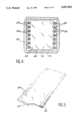
- FIG. 3 shows a schematic, cross-section view of a sensor according to the invention
- FIG. 4 shows a schematic sectional view along BB of the sensor of FIG. 3;
- FIG. 5 shows a schematic view, in perspective, of one of the connection means used in the sensor of the invention.
- the sensor according to the invention shown schematically in a cross-section in FIG. 3, comprises a sealed package 20, made of an electrically insulating material, for example a plastic material.
- This package has a front face 21, provided with a window 22, made of an electrically insulating and transparent material, such as a plastic material or glass.
- the imperviousness between the package 20 and the window 22 is provided by suitable means such as bonding for example.
- the window 22 receives light rays R, coming from a part of the inside of an object or an organ of the human body.
- the inside of the package contains, between the back 23 and the window 22, a stack arrangement which comprises an insulating support 24, made of ceramic for example, and a set of photosensitive elements 25 with a semiconducting substrate 26.
- the photosensitive elements form a photosensitive surface S1, which can be seen more clearly in the section BB of FIG. 4. This surface is bounded by a periphery P1 having contacts such as 27 for connection with the photosensitive elements 25.
- These elements are not shown in detail. They may consist of photodiodes, possibly associated with charge-coupled devices (CCDs) forming a photosensitive matrix of the surface S1.
- CCDs charge-coupled devices
- This sensor also has connection means to connect the contacts 27 with connection terminals 28, enabling electrical supply to the photosensitive elements and enabling the collection of the electrical signals given by these elements when they are illuminated by the light rays R, coming from inside the object or organ for which it is sought to obtain an image. Of course, this picture is obtained by processing the signals collected at the terminals 28.
- the connections 28 go through the back 23 of the package20 and, according to the invention, also go through the insulating support 24. Each end 30 of each terminal emerges from the insulating support and reaches that face of this support which faces the photosensitive elements 25 and the contacts 27.
- the semiconducting substrate 26 (made of silicon for example) is placed facing the window 22 while the photosensitive elements are placed facing the insulating support 24.
- a reverse arrangement is chosen as can be seen in FIG. 1.
- the semiconducting substrate 7 is facing the insulating support 5 while the photosensitive elements 6 are facing the window 3.
- the result thereof is that, in the prior art sensor, the light rays R are directly received by the photosensitive elements 6 after they have gone through the window 3.
- the sensor of the invention FIGS.
- the light rays R are received by the photosensitive elements 25, after they have crossed the window 22 and the semiconducting substrate 26, obtained by thinning down the standard semiconducting substrate which, herein, has a thickness which is far smaller than that of the known sensor (10 to 15 microns instead of severaltens of microns). It is precisely this reverse arrangement that makes it possible to very greatly increase the area of the photosensitive surface within the package as can be seen in FIG. 4.
- the contacts 27 are located so that they face the back of the package and the corresponding connection terminals 28. This makes it possible, as shall be seen further below in detail, to reduce the space occupied by the connection means usedto connect these contacts and these terminals respectively.
- connection means are, herein, respectively interposed between these contacts 27 and the terminals 28 which correspond to them.
- connection means comprise spacers 29 made of a conductive material These spacers are respectively interposed between the contacts 27and the ends 30 of the corresponding terminals 28. Each spacer is in contact with the end 30 of the corresponding terminal 28, owing to the mechanical pressure exerted by the package on the window 22 which itself rests on the substrate 26.
- These spacers may be formed, in this embodiment, by indium balls obtained by growth under vacuum on the contacts 27. When the package is molded around the stack arrangement, these balls are slightly crushed owing to the mechanical pressure exerted by the package on the window, and good electrical contact is thus providedbetween these balls and the ends 30 of the terminals 28.
- spacers may also be formed by a conductive bonder, such as an epoxy resin containing silver for example.
- FIG. 5 gives a schematic view, in perspective, of another embodiment of theconnection means interposed between the contacts 27 and the ends 30 of the terminals 28.
- these connection means are formed by an insulating sheet 31 which has zones 32 of a conducting material. These zones are respectively located so that they face contacts 27 and the ends 30 of the corresponding terminals 28.
- the conducting zones are metallic (made of copper for example).
- the insulating sheet 31 may be made of an elastomer material. During the assembly of the sensor, this insulating sheet 31 is interposed between the set of photosensitive elements 25 and the ends 30 of the terminals 28. The pressure exerted by the package on the window 22 provides for good contact among the conducting zones 32, theends 30 of the terminals 28 and the contacts 27.
- the area of the surface S1 of the set of photosensitive elements can be at least two times smaller than the area ofthe surface S of these elements in the prior art sensor. The same is true for the number of connection terminals which is far greater than in the prior art sensor.
Abstract
Description
Claims (7)
Applications Claiming Priority (2)
| Application Number | Priority Date | Filing Date | Title |
|---|---|---|---|
| FR8800679A FR2626408B1 (en) | 1988-01-22 | 1988-01-22 | LOW-SIZE IMAGE SENSOR |
| FR8800679 | 1988-01-22 |
Related Parent Applications (1)
| Application Number | Title | Priority Date | Filing Date |
|---|---|---|---|
| US07298903 Continuation | 1989-01-19 |
Publications (1)
| Publication Number | Publication Date |
|---|---|
| US5051802A true US5051802A (en) | 1991-09-24 |
Family
ID=9362509
Family Applications (1)
| Application Number | Title | Priority Date | Filing Date |
|---|---|---|---|
| US07/563,826 Expired - Lifetime US5051802A (en) | 1988-01-22 | 1990-08-06 | Compact image sensor |
Country Status (5)
| Country | Link |
|---|---|
| US (1) | US5051802A (en) |
| EP (1) | EP0325525B1 (en) |
| JP (1) | JPH023969A (en) |
| DE (1) | DE68900072D1 (en) |
| FR (1) | FR2626408B1 (en) |
Cited By (37)
| Publication number | Priority date | Publication date | Assignee | Title |
|---|---|---|---|---|
| US5198881A (en) * | 1989-12-28 | 1993-03-30 | Massachusetts Institute Of Technology | Barrier layer device processing |
| US5233178A (en) * | 1991-03-29 | 1993-08-03 | Nec Corporation | Contact type image sensor and method of producing the same |
| DE4424541A1 (en) * | 1994-01-24 | 1995-08-03 | Gold Star Electronics | Solid-state image pick=up element mfg. method for video camera |
| US5801849A (en) * | 1996-10-21 | 1998-09-01 | Telesensory Corporation | Image reading device and document scanning system |
| WO2000011723A1 (en) * | 1998-08-21 | 2000-03-02 | Gentex Corporation | Package for an optical sensor |
| EP1104182A1 (en) * | 1999-11-27 | 2001-05-30 | STMicroelectronics Limited | Improved image sensor devices for Incorporation into endoscopes |
| US6407381B1 (en) * | 2000-07-05 | 2002-06-18 | Amkor Technology, Inc. | Wafer scale image sensor package |
| GB2374726A (en) * | 2001-04-20 | 2002-10-23 | Kingpak Tech Inc | Stacked structure of an image sensor having image sensing chip located above integrated circuit |
| US6492699B1 (en) | 2000-05-22 | 2002-12-10 | Amkor Technology, Inc. | Image sensor package having sealed cavity over active area |
| US6503780B1 (en) * | 2000-07-05 | 2003-01-07 | Amkor Technology, Inc. | Wafer scale image sensor package fabrication method |
| US20030013328A1 (en) * | 2001-05-22 | 2003-01-16 | Andrade Thomas L. | Connection assembly for integrated circuit sensors |
| US6512219B1 (en) | 2000-01-25 | 2003-01-28 | Amkor Technology, Inc. | Fabrication method for integrally connected image sensor packages having a window support in contact with the window and active area |
| US20030020495A1 (en) * | 2001-05-22 | 2003-01-30 | Andrade Thomas L. | Surface capacitance sensor system using buried stimulus electrode |
| US6515269B1 (en) | 2000-01-25 | 2003-02-04 | Amkor Technology, Inc. | Integrally connected image sensor packages having a window support in contact with a window and the active area |
| US20030062621A1 (en) * | 1998-07-14 | 2003-04-03 | Infineon Technologies Ag | Method of producing a biometric sensor |
| DE102004055677A1 (en) * | 2004-11-18 | 2006-06-01 | Fraunhofer-Gesellschaft zur Förderung der angewandten Forschung e.V. | Compound chip carrier, as an image sensor for military night sights and the like, has a chip bonded to the substrate with contact surfaces and conductive zones through the substrate |
| US20070034995A1 (en) * | 2003-06-05 | 2007-02-15 | Sanyo Electric Co., Ltd. | Optical Semiconductor Device and Method of Manufacturing the Same |
| US7256589B2 (en) | 2001-04-27 | 2007-08-14 | Atrua Technologies, Inc. | Capacitive sensor system with improved capacitance measuring sensitivity |
| US20080157252A1 (en) * | 2006-12-27 | 2008-07-03 | Lite-On Semiconductor Corp. | Optical sensor package |
| US20080308928A1 (en) * | 2007-06-13 | 2008-12-18 | Industrial Technology Research Institute | Image sensor module with a three-dimensional die-stacking structure |
| US20100032830A1 (en) * | 2008-08-06 | 2010-02-11 | Industrial Technology Research Institute | Three-dimensional conducting structure and method of fabricating the same |
| US20100065961A1 (en) * | 2008-09-18 | 2010-03-18 | Klaus Elian | Electronic Device and Method of Manufacturing Same |
| US20100102213A1 (en) * | 2008-10-27 | 2010-04-29 | Itt Manufacturing Enterprises, Inc. | Apparatus and method for aligning an image sensor |
| US20120029287A1 (en) * | 2009-03-06 | 2012-02-02 | Olympus Winter & Ibe Gmbh | Surgical instrument |
| US20140077395A1 (en) * | 1998-02-06 | 2014-03-20 | Invensas Corporation | Integrated circuit device |
| TWI505427B (en) * | 2010-03-15 | 2015-10-21 | Hk Applied Science & Tech Res | Electronic device package and methods of manufacturing an electronic device package |
| US10269853B2 (en) * | 2014-12-11 | 2019-04-23 | Invensas Corporation | Image sensor device |
| US11069734B2 (en) | 2014-12-11 | 2021-07-20 | Invensas Corporation | Image sensor device |
| US11387214B2 (en) | 2017-06-15 | 2022-07-12 | Invensas Llc | Multi-chip modules formed using wafer-level processing of a reconstituted wafer |
| US11462419B2 (en) | 2018-07-06 | 2022-10-04 | Invensas Bonding Technologies, Inc. | Microelectronic assemblies |
| US11538781B2 (en) | 2020-06-30 | 2022-12-27 | Adeia Semiconductor Bonding Technologies Inc. | Integrated device packages including bonded structures |
| US11728273B2 (en) | 2020-09-04 | 2023-08-15 | Adeia Semiconductor Bonding Technologies Inc. | Bonded structure with interconnect structure |
| US11742314B2 (en) | 2020-03-31 | 2023-08-29 | Adeia Semiconductor Bonding Technologies Inc. | Reliable hybrid bonded apparatus |
| US11742315B2 (en) | 2017-04-21 | 2023-08-29 | Adeia Semiconductor Bonding Technologies Inc. | Die processing |
| US11764177B2 (en) | 2020-09-04 | 2023-09-19 | Adeia Semiconductor Bonding Technologies Inc. | Bonded structure with interconnect structure |
| US11855064B2 (en) | 2018-02-15 | 2023-12-26 | Adeia Semiconductor Bonding Technologies Inc. | Techniques for processing devices |
| US11955463B2 (en) | 2019-06-26 | 2024-04-09 | Adeia Semiconductor Bonding Technologies Inc. | Direct bonded stack structures for increased reliability and improved yield in microelectronics |
Families Citing this family (4)
| Publication number | Priority date | Publication date | Assignee | Title |
|---|---|---|---|---|
| JP3017780B2 (en) * | 1990-09-10 | 2000-03-13 | 株式会社東芝 | Electronic endoscope imaging device |
| US5418566A (en) * | 1990-09-10 | 1995-05-23 | Kabushiki Kaisha Toshiba | Compact imaging apparatus for electronic endoscope with improved optical characteristics |
| US6757483B1 (en) | 1996-03-19 | 2004-06-29 | Pioneer Electronic Corporation | Information recording medium with aggregate attribute information recorded in video manager, apparatus for recording the same and apparatus for reproducing the same |
| FR2819103B1 (en) * | 2000-12-29 | 2003-12-12 | St Microelectronics Sa | OPTICAL SEMICONDUCTOR PACKAGE WITH TRANSPARENT PELLET AND MANUFACTURING METHOD THEREOF |
Citations (6)
| Publication number | Priority date | Publication date | Assignee | Title |
|---|---|---|---|---|
| US3456159A (en) * | 1963-08-08 | 1969-07-15 | Ibm | Connections for microminiature functional components |
| JPS5840870A (en) * | 1981-09-03 | 1983-03-09 | Sanyo Electric Co Ltd | Light receiving device |
| JPS58107788A (en) * | 1981-12-21 | 1983-06-27 | Mitsubishi Electric Corp | Solid-state color image sensor |
| JPS5947774A (en) * | 1982-09-10 | 1984-03-17 | Fuji Electric Co Ltd | Photo semiconductor device |
| JPS5996751A (en) * | 1982-11-26 | 1984-06-04 | Hitachi Ltd | Semiconductor device |
| FR2565408A1 (en) * | 1984-05-30 | 1985-12-06 | Thomson Csf | Device containing an integrated circuit wafer surmounted by an insulating slab acting as package |
-
1988
- 1988-01-22 FR FR8800679A patent/FR2626408B1/en not_active Expired - Lifetime
-
1989
- 1989-01-17 EP EP89400130A patent/EP0325525B1/en not_active Expired - Lifetime
- 1989-01-17 DE DE8989400130T patent/DE68900072D1/en not_active Expired - Lifetime
- 1989-01-20 JP JP1011780A patent/JPH023969A/en active Pending
-
1990
- 1990-08-06 US US07/563,826 patent/US5051802A/en not_active Expired - Lifetime
Patent Citations (6)
| Publication number | Priority date | Publication date | Assignee | Title |
|---|---|---|---|---|
| US3456159A (en) * | 1963-08-08 | 1969-07-15 | Ibm | Connections for microminiature functional components |
| JPS5840870A (en) * | 1981-09-03 | 1983-03-09 | Sanyo Electric Co Ltd | Light receiving device |
| JPS58107788A (en) * | 1981-12-21 | 1983-06-27 | Mitsubishi Electric Corp | Solid-state color image sensor |
| JPS5947774A (en) * | 1982-09-10 | 1984-03-17 | Fuji Electric Co Ltd | Photo semiconductor device |
| JPS5996751A (en) * | 1982-11-26 | 1984-06-04 | Hitachi Ltd | Semiconductor device |
| FR2565408A1 (en) * | 1984-05-30 | 1985-12-06 | Thomson Csf | Device containing an integrated circuit wafer surmounted by an insulating slab acting as package |
Non-Patent Citations (6)
| Title |
|---|
| Patent Abstracts of Japan, vol. 7, No. 214 (E 199) 1359 , Sep. 21, 1983. * |
| Patent Abstracts of Japan, vol. 7, No. 214 (E-199)[1359], Sep. 21, 1983. |
| Patent Abstracts of Japan, vol. 8, No. 139 (E 253) 1576 , Jun. 28, 1984. * |
| Patent Abstracts of Japan, vol. 8, No. 139 (E-253)[1576], Jun. 28, 1984. |
| Patents Abstracts of Japan, vol. 7, No. 123 (E 178) 1268 , May 27, 1983. * |
| Patents Abstracts of Japan, vol. 7, No. 123 (E-178)[1268], May 27, 1983. |
Cited By (51)
| Publication number | Priority date | Publication date | Assignee | Title |
|---|---|---|---|---|
| US5198881A (en) * | 1989-12-28 | 1993-03-30 | Massachusetts Institute Of Technology | Barrier layer device processing |
| US5233178A (en) * | 1991-03-29 | 1993-08-03 | Nec Corporation | Contact type image sensor and method of producing the same |
| DE4424541A1 (en) * | 1994-01-24 | 1995-08-03 | Gold Star Electronics | Solid-state image pick=up element mfg. method for video camera |
| US5801849A (en) * | 1996-10-21 | 1998-09-01 | Telesensory Corporation | Image reading device and document scanning system |
| US20140077395A1 (en) * | 1998-02-06 | 2014-03-20 | Invensas Corporation | Integrated circuit device |
| US9530945B2 (en) * | 1998-02-06 | 2016-12-27 | Invensas Corporation | Integrated circuit device |
| US20030062621A1 (en) * | 1998-07-14 | 2003-04-03 | Infineon Technologies Ag | Method of producing a biometric sensor |
| US6836953B2 (en) * | 1998-07-14 | 2005-01-04 | Infineon Technologies Ag | Method of producing a biometric sensor |
| WO2000011723A1 (en) * | 1998-08-21 | 2000-03-02 | Gentex Corporation | Package for an optical sensor |
| US6130448A (en) * | 1998-08-21 | 2000-10-10 | Gentex Corporation | Optical sensor package and method of making same |
| US6621616B1 (en) | 1998-08-21 | 2003-09-16 | Gentex Corporation | Devices incorporating electrochromic elements and optical sensors |
| EP1104182A1 (en) * | 1999-11-27 | 2001-05-30 | STMicroelectronics Limited | Improved image sensor devices for Incorporation into endoscopes |
| US6512219B1 (en) | 2000-01-25 | 2003-01-28 | Amkor Technology, Inc. | Fabrication method for integrally connected image sensor packages having a window support in contact with the window and active area |
| US6515269B1 (en) | 2000-01-25 | 2003-02-04 | Amkor Technology, Inc. | Integrally connected image sensor packages having a window support in contact with a window and the active area |
| US6492699B1 (en) | 2000-05-22 | 2002-12-10 | Amkor Technology, Inc. | Image sensor package having sealed cavity over active area |
| US6407381B1 (en) * | 2000-07-05 | 2002-06-18 | Amkor Technology, Inc. | Wafer scale image sensor package |
| US6503780B1 (en) * | 2000-07-05 | 2003-01-07 | Amkor Technology, Inc. | Wafer scale image sensor package fabrication method |
| GB2374726A (en) * | 2001-04-20 | 2002-10-23 | Kingpak Tech Inc | Stacked structure of an image sensor having image sensing chip located above integrated circuit |
| US7256589B2 (en) | 2001-04-27 | 2007-08-14 | Atrua Technologies, Inc. | Capacitive sensor system with improved capacitance measuring sensitivity |
| US20030013328A1 (en) * | 2001-05-22 | 2003-01-16 | Andrade Thomas L. | Connection assembly for integrated circuit sensors |
| US20030020495A1 (en) * | 2001-05-22 | 2003-01-30 | Andrade Thomas L. | Surface capacitance sensor system using buried stimulus electrode |
| US7259573B2 (en) | 2001-05-22 | 2007-08-21 | Atrua Technologies, Inc. | Surface capacitance sensor system using buried stimulus electrode |
| US20070034995A1 (en) * | 2003-06-05 | 2007-02-15 | Sanyo Electric Co., Ltd. | Optical Semiconductor Device and Method of Manufacturing the Same |
| US7728438B2 (en) * | 2003-06-05 | 2010-06-01 | Sanyo Electric Co., Ltd. | Optical semiconductor device and method of manufacturing the same |
| DE102004055677A1 (en) * | 2004-11-18 | 2006-06-01 | Fraunhofer-Gesellschaft zur Förderung der angewandten Forschung e.V. | Compound chip carrier, as an image sensor for military night sights and the like, has a chip bonded to the substrate with contact surfaces and conductive zones through the substrate |
| US20080157252A1 (en) * | 2006-12-27 | 2008-07-03 | Lite-On Semiconductor Corp. | Optical sensor package |
| US7663231B2 (en) | 2007-06-13 | 2010-02-16 | Industrial Technology Research Institute | Image sensor module with a three-dimensional die-stacking structure |
| US20080308928A1 (en) * | 2007-06-13 | 2008-12-18 | Industrial Technology Research Institute | Image sensor module with a three-dimensional die-stacking structure |
| US8193632B2 (en) | 2008-08-06 | 2012-06-05 | Industrial Technology Research Institute | Three-dimensional conducting structure and method of fabricating the same |
| US20100032830A1 (en) * | 2008-08-06 | 2010-02-11 | Industrial Technology Research Institute | Three-dimensional conducting structure and method of fabricating the same |
| US20100065961A1 (en) * | 2008-09-18 | 2010-03-18 | Klaus Elian | Electronic Device and Method of Manufacturing Same |
| US7964448B2 (en) | 2008-09-18 | 2011-06-21 | Infineon Technologies Ag | Electronic device and method of manufacturing same |
| US20100102213A1 (en) * | 2008-10-27 | 2010-04-29 | Itt Manufacturing Enterprises, Inc. | Apparatus and method for aligning an image sensor |
| US7880127B2 (en) * | 2008-10-27 | 2011-02-01 | Itt Manufacturing Enterprises, Inc. | Apparatus and method for aligning an image sensor including a header alignment means |
| US20120029287A1 (en) * | 2009-03-06 | 2012-02-02 | Olympus Winter & Ibe Gmbh | Surgical instrument |
| US9839346B2 (en) * | 2009-03-06 | 2017-12-12 | Olympus Winter & Ibe Gmbh | Surgical instrument |
| TWI505427B (en) * | 2010-03-15 | 2015-10-21 | Hk Applied Science & Tech Res | Electronic device package and methods of manufacturing an electronic device package |
| US11069734B2 (en) | 2014-12-11 | 2021-07-20 | Invensas Corporation | Image sensor device |
| US11935907B2 (en) | 2014-12-11 | 2024-03-19 | Adeia Semiconductor Technologies Llc | Image sensor device |
| US10269853B2 (en) * | 2014-12-11 | 2019-04-23 | Invensas Corporation | Image sensor device |
| US10847562B2 (en) | 2014-12-11 | 2020-11-24 | Invensas Corporation | Image sensor device |
| US11742315B2 (en) | 2017-04-21 | 2023-08-29 | Adeia Semiconductor Bonding Technologies Inc. | Die processing |
| US11387214B2 (en) | 2017-06-15 | 2022-07-12 | Invensas Llc | Multi-chip modules formed using wafer-level processing of a reconstituted wafer |
| US11855064B2 (en) | 2018-02-15 | 2023-12-26 | Adeia Semiconductor Bonding Technologies Inc. | Techniques for processing devices |
| US11462419B2 (en) | 2018-07-06 | 2022-10-04 | Invensas Bonding Technologies, Inc. | Microelectronic assemblies |
| US11955463B2 (en) | 2019-06-26 | 2024-04-09 | Adeia Semiconductor Bonding Technologies Inc. | Direct bonded stack structures for increased reliability and improved yield in microelectronics |
| US11742314B2 (en) | 2020-03-31 | 2023-08-29 | Adeia Semiconductor Bonding Technologies Inc. | Reliable hybrid bonded apparatus |
| US11538781B2 (en) | 2020-06-30 | 2022-12-27 | Adeia Semiconductor Bonding Technologies Inc. | Integrated device packages including bonded structures |
| US11631647B2 (en) | 2020-06-30 | 2023-04-18 | Adeia Semiconductor Bonding Technologies Inc. | Integrated device packages with integrated device die and dummy element |
| US11728273B2 (en) | 2020-09-04 | 2023-08-15 | Adeia Semiconductor Bonding Technologies Inc. | Bonded structure with interconnect structure |
| US11764177B2 (en) | 2020-09-04 | 2023-09-19 | Adeia Semiconductor Bonding Technologies Inc. | Bonded structure with interconnect structure |
Also Published As
| Publication number | Publication date |
|---|---|
| FR2626408A1 (en) | 1989-07-28 |
| FR2626408B1 (en) | 1990-05-11 |
| EP0325525B1 (en) | 1991-05-08 |
| DE68900072D1 (en) | 1991-06-13 |
| JPH023969A (en) | 1990-01-09 |
| EP0325525A1 (en) | 1989-07-26 |
Similar Documents
| Publication | Publication Date | Title |
|---|---|---|
| US5051802A (en) | Compact image sensor | |
| US6727431B2 (en) | Optical module, circuit board and electronic device | |
| US5418566A (en) | Compact imaging apparatus for electronic endoscope with improved optical characteristics | |
| JPH10335624A (en) | Rear-irradiation photodetector and manufacture thereof | |
| US8319871B2 (en) | Solid-state imaging device, its production method, camera with the solid-state imaging device, and light receiving chip | |
| JP2607542B2 (en) | Solid-state imaging device | |
| US6603107B2 (en) | Image pickup device and portable telephone | |
| US6172351B1 (en) | Photoelectric integrated circuit device | |
| JP2006032561A (en) | Semiconductor image sensor module | |
| US4772951A (en) | Solid state image sensor with cell array of amorphous semiconductor photoelectric converting elements | |
| JPS61123288A (en) | Solid-state pick up device | |
| JPS61134187A (en) | Solid-state image pickup device | |
| JPH1012851A (en) | Radiation image pickup device | |
| JPH0226080A (en) | Semiconductor device | |
| JPS61131690A (en) | Solid-state image pick-up device | |
| US6791842B2 (en) | Image sensor structure | |
| US20070205480A1 (en) | Semiconductor Device | |
| KR100502212B1 (en) | Image Sensor And Manufacturing Method Thereof | |
| US20020060287A1 (en) | Structure of a photosensor and method for packaging the same | |
| JP3817859B2 (en) | Imaging device | |
| JP4799746B2 (en) | Radiation detector module | |
| JPH09326479A (en) | Solid-state image pick-up device | |
| JPH07231074A (en) | Solid-state image sensing module | |
| JP2847093B2 (en) | Video camera | |
| JP2001320035A (en) | Two-dimensional radiation detector |
Legal Events
| Date | Code | Title | Description |
|---|---|---|---|
| AS | Assignment |
Owner name: THOMSON-CSF, FRANCE Free format text: ASSIGNMENT OF ASSIGNORS INTEREST.;ASSIGNORS:PROST, ROGER;CHABBAL, JEAN;REEL/FRAME:005751/0814 Effective date: 19890110 Owner name: THOMSON-CSF, FRANCE Free format text: ASSIGNMENT OF ASSIGNORS INTEREST;ASSIGNORS:PROST, ROGER;CHABBAL, JEAN;REEL/FRAME:005751/0814 Effective date: 19890110 |
|
| STCF | Information on status: patent grant |
Free format text: PATENTED CASE |
|
| FEPP | Fee payment procedure |
Free format text: PAYOR NUMBER ASSIGNED (ORIGINAL EVENT CODE: ASPN); ENTITY STATUS OF PATENT OWNER: LARGE ENTITY |
|
| FPAY | Fee payment |
Year of fee payment: 4 |
|
| FPAY | Fee payment |
Year of fee payment: 8 |
|
| FPAY | Fee payment |
Year of fee payment: 12 |