US5083294A - Semiconductor memory device having a redundancy - Google Patents
Semiconductor memory device having a redundancy Download PDFInfo
- Publication number
- US5083294A US5083294A US07/562,512 US56251290A US5083294A US 5083294 A US5083294 A US 5083294A US 56251290 A US56251290 A US 56251290A US 5083294 A US5083294 A US 5083294A
- Authority
- US
- United States
- Prior art keywords
- memory cell
- redundant
- column
- cell array
- main memory
- Prior art date
- Legal status (The legal status is an assumption and is not a legal conclusion. Google has not performed a legal analysis and makes no representation as to the accuracy of the status listed.)
- Expired - Lifetime
Links
Images


Classifications
-
- G—PHYSICS
- G11—INFORMATION STORAGE
- G11C—STATIC STORES
- G11C29/00—Checking stores for correct operation ; Subsequent repair; Testing stores during standby or offline operation
-
- G—PHYSICS
- G11—INFORMATION STORAGE
- G11C—STATIC STORES
- G11C29/00—Checking stores for correct operation ; Subsequent repair; Testing stores during standby or offline operation
- G11C29/70—Masking faults in memories by using spares or by reconfiguring
- G11C29/78—Masking faults in memories by using spares or by reconfiguring using programmable devices
- G11C29/80—Masking faults in memories by using spares or by reconfiguring using programmable devices with improved layout
- G11C29/808—Masking faults in memories by using spares or by reconfiguring using programmable devices with improved layout using a flexible replacement scheme
Definitions
- the present invention generally relates to semiconductor memory devices and more particularly to a semiconductor memory device having a redundant construction.
- a redundant construction wherein redundant memory cell columns are provided in the memory cell array.
- a map of defective memory cells in the memory cell array is stored in a read-only memory and the like and the address signal addressing the defective memory cell in the array is converted, on the basis of the map, to an address signal which addresses a normal, defect-free memory cell. More specifically, when there is an address signal addressing a defective memory cell, the memory cell column including the defective memory cell column is switched to another, redundant memory cell column. Thereby, a normal memory cell is used in place of the addressed defective memory cell and the memory device operates as if it is a defect-free device.
- the memory cell array are divided into a number of blocks each containing a number of memory cells arranged in a row and column formation.
- a memory cell is connected to a bit line and a divided word line which is a word line branched from a main word line.
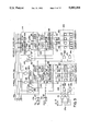
- FIG. 1 shows such a conventional semiconductor memory device having the divided word line construction.
- the memory cell array 1 is divided into a number of blocks or memory cell columns 2, 3, 4, . . . each containing a number of memory cells 15, 16, 17, . . . arranged therein in a row and column formation.
- a number of word line drivers 19 each connected to a main word line MWL are provided, wherein only one word line driver 19 is illustrated in the drawing.
- the main word line MWL extends throughout the memory cell array 1, passing through the blocks 2-4.
- the word line driver 19 is supplied with a word line selection signal addressing one of the main word lines MWL from an X-decoder 24 along a bus 24a, in response to address data ADDRESS1 supplied to the X-decoder 24.
- a Y-decoder 25 to which a second address data ADDRESS2 is supplied, wherein the Y-decoder 25 is connected to bit line drivers 11, 12, 13, . . . via an address bus 25a for selectively addressing a pair of bit lines BL and BL via respective read/write controllers 6, 7, 8, . . . .
- the bit line decoder 11 energizes the controller 6 in response to the output of the Y-decoder 25, and thereby the bit line BL and BL connected to the addressed memory cell 15 are selected.
- the main word line driver 19 is energized in response to the output of the X-decoder 24 and the main word line driver 19 selects the main word line MWL connected thereto.
- a gate device 20 which is supplied with the output of the main word line driver 19 and the output of the bit line driver 11 for producing an output which is supplied to the memory cell 15 via a divided word line DWL.
- the gate device 20 is energized and the divided word line DWL connected to the addressed memory cell 15 is selected.
- the bit line driver 11 and the main word line driver -9 are constructed as a NAND gate while the gate device 20 is constructed as a NOR gate.
- the divided word line DWL is selected in response to the low level output of the devices 11 and 19.
- the data in the memory cell 15 is transferred along the bit lines BL and BL to the controller such as the controller 5, and from there transferred further to a sense amplifier 10a along a read bus 26.
- the data supplied to a data input terminal DIN is transferred to to the selected controller such as the controller 6 along a write bus 27 after amplification in a write amplifier 10b, and the data is further transferred to the memory cell such as the memory cell 15 along the bit lines BL and BL.
- the length of the word line connected to the memory cell can be reduced and thereby the access time of the memory device is significantly reduced as a result of the reduction of parasitic capacitance associated with the memory cells connected to the word line.
- the foregoing redundant construction is employed.
- the redundant memory cells are provided in each of the blocks 2-4 and operation of the bit line driver is controlled such that an alternative bit line or memory cell column is selected when a bit line which is connected to one or more defective memory cells is addressed.
- a read-only memory not illustrated is provided in cooperation with each of the bit line drivers 11-13.
- Another object of the present invention is to provide a semiconductor memory device having a divided word line construction and a redundant construction at the same time, wherein the efficiency of use of the memory cell for the redundancy purpose is improved and the overall chip size is reduced.
- Another object of the present invention is to provide a semiconductor memory device comprising a memory cell array in which the memory cell array is divided into a number of blocks each having divided word lines and bit lines extending in the block, wherein one block in the memory cell array is used as a redundant memory cell block such that when a defective memory cell in one block is addressed, the memory cell column including the defective memory cell in the block is replaced with a memory cell column in the redundant memory cell block.
- the redundant column is used commonly with respect to all the blocks in the memory cell array and the efficiency of use of the redundant memory cell column is significantly improved. It should be noted that the provision of redundant column in each of the blocks can be eliminated by the present construction and the size of the chip of the semiconductor memory device is significantly reduced.
- FIG. 1 is a block diagram showing a conventional semiconductor memory device
- FIG. 2 is a diagram showing a first embodiment of the semiconductor memory device according to the present invention.
- FIG. 3 is a block diagram showing a part of the semiconductor memory device of FIG. 2;
- FIGS. 4A and 4B are circuit diagrams showing the construction of programm,able switches used in the semiconductor memory device of FIG. 3;
- FIGS. 5A-5C are circuit diagrams showing various circuit elements used in the semiconductor memory device of FIG. 3;
- FIG. 6 is a graph showing the effect of the present invention.
- FIG. 7 is a circuit diagram showing a second embodiment of the present invention.
- FIG. 8 is a circuit diagram showing a third embodiment of the present invention.
- FIG. 9 is a circuit diagram showing a fourth embodiment of the present invention.
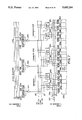
- FIG. 2 shows a first embodiment of the semiconductor memory device of the present invention.
- the semiconductor memory device comprises a memory cell array 100 similar to the memory cell array 1 of FIG. 1 except that each of the blocks 102-104 does not contain the redundant columns and that there is provided a redundant block 105 including a number of memory cells 18 arranged in row and column formation.
- This redundant block 105 is formed exclusively from memory cells forming the redundant columns.
- Each of the memory cells 18 is connected, in the row direction, commonly to a divided word line DWL extending through the redundant block 105, and the divided word line DWL is connected to a main word line MWL extending throughout the memory cell array 100 via a gate device 23.
- the gate device 23 comprises a NOR device having a first input terminal to which the main word line MWL is connected and a second input terminal to which a negative or low level bias voltage is applied constantly.
- the bit lines in the block 102 are connected to a read/write controller 106 similar to the read/write controller 6 of FIG. 1, the bit lines in the block 103 are connected to a read/write controller 107 similar to the read/write controller 7 of FIG. 1, the bit lines in the block 104 are connected to a read/write controller 108 similar to the read/write controller 8 of FIG. I, while the bit lines in the redundant block 105 are connected to a read/write controller 109 to be described later.
- the read/write controllers 106-109 are connected to the read bus 26 and the write bus 27 which are connected respectively to the sense amplifier 10a and the write amplifier 10b.
- the bit line drivers 111-114 are programmable logic devices for producing an output in response to the address data supplied to the Y-decoder 25 in accordance with a program stored therein.
- the bit line drivers 111 etc. are operated such that a read/write controller such as the read/write controller 106 connected to the bit line to which the addressed memory cell is connected, is enabled selectively in response to the address data to the Y-decoder 25, while other read/write amplifiers are disabled.
- the addressed memory cell for example the memory cell 15, is addressed.
- the selection of the divided word line DWL connected to the memory cell 15 is made via the gate device 20 in response to the output of the word line driver 19 and the bit line driver 111.
- the bit line driver 111 is prohibited from enabling the read/write controller 106 as a result of the programmed operation which takes place in accordance with the program stored therein.
- one of the bit line drivers such as the bit line driver 114 cooperating with the read/write controller for the redundant block 105 is driven so as to enable a read/write controller cooperating with the bit lines in the block 105 such as the read/write controller 109, also under the control of a program stored in the driver 114.
- a memory cell column in the redundant block 105 is addressed in place of the memory cell column in the block 102 and the semiconductor memory device operates as if it is a memory device free from defective memory cells.
- FIG. 3 shows an essential part of the semiconductor memory device of FIG. 2. For the sake of simplicity of the drawing, only a part of the block 102 and block 105 are shown together with related peripheral circuits.
- the address bus 25a comprises a number of line pairs respectively designated as Y0 and /Y0, Y1 and /Y1, Y2 and /Y2, . . .
- the bit line driver 111 comprises NOR gates 86-89, wherein the NOR gate 86 has a first input terminal connected to the line Y0 and a second input terminal connected to the line /Y2, the NOR gate 87 has a first input terminal connected to the line /Y0 and a second input terminal to the line /Y2, the NOR gate 88 has a first input terminal connected to the Y1 line and a second input terminal connected to the /Y2 line, and the NOR gate 89 has a first input terminal connected to the /Y1 line and a second input terminal connected to the /Y2 line.
- the NOR gate 86 has an output terminal connected to a column switch circuit 97 to which a pair of bit lines BL2 and BL2 are connected and further to a column switch circuit 99 to which a pair of bit lines BL4 and BL4 are connected.
- the NOR gate 87 has an output terminal connected to a column switch circuit 96 to which a pair of bit lines BL1 and are connected and to a column switch circuit 98 to which a pair of bit lines BL3 and BL3 are connected.
- a local write amplifier 92 and a local sense amplifier 94 are connected electrically in parallel with each other, wherein the column switch 97 connects the bit lines BL2 and BL2 to the local sense amplifier 94 and the local write amplifier 92 in response to the output of the NOR gate 86.
- the column switch 97 is enabled when there is a low level state on both of the lines Y0 and /Y2.
- the column switch circuit 99 is enabled and the bit lines BL4 and BL4 are connected to the local sense amplifier 95 and the local write amplifier 93.
- the local sense amplifiers 94 and 95 are connected commonly to the read bus 26 while the local write amplifiers 92 and 93 are connected commonly to the write bus 27.
- the local write amplifiers 92 and 93, and the local sense amplifiers 94 and 95 are driven in response to the logic state appearing on the lines /Y2, Y1, and /Y1. More specifically, a NOR gate 88 having an input terminal connected to the line Y1 and another input terminal connected to the line /Y2 is provided such that an output signal thereof is supplied to the local write amplifier 92 and further to the local sense amplifier 94 via a programmable switch 90a. Similarly, another NOR gate 89 having an input terminal connected to the line /Y1 and another input terminal connected to the line /Y2 is provided such that an output signal thereof is supplied to the local write amplifier 93 and further to the local sense amplifier 95 via a programmable switch 90b.
- the local write amplifier 92 is enabled and transfers the logic data on the write bus 27 to the bit line pair BL1 and BL1 or to the bit line pair BL2 and BL2, depending on the state of the column switches 96 and 97.
- the write amplifier 10b is enabled in response to a write enable signal WE supplied thereto, the data supplied to an input terminal D IN of the write amplifier 94 is transferred to the bit lines via the write bus 27, the local write amplifier 92 and the column switch 96 or 97.
- the local sense amplifier 10a is enabled and transfers the logic data on the bit line pair BL1 and BL1 or the bit line pair BL2 and BL2 to the sense amplifier 10b along the read bus 26, depending on the state of the column switches 96 and 97. Further, the data on the read bus 26 is transferred to an output terminal D OUT of the sense amplifier 10a.
- NOR gate 89 and a programmable switch 90b are provided respectively in correspondence to the NOR gate 88 and the programmable switch 90a described previously.
- the operation of this part is substantially identical to the part including the NOR gate 88, the programmable switch 90a, the local write amplifier 92, the local sense amplifier 94, the column switches 96 and 97, and the bit line pairs BL1 and BL1 and BL2 and BL2 which are described already, the description thereof will not be repeated.
- bit lines BL1, BL1, BL2 and BL2 form one subblock, SUBBLOCK1, in the block of memory cell while the bit lines BL3, BL3, BL4 and BL4 form another subblock, SUBBLOCK2, in the same block 102.
- the selection of the subblock is made by the NOR gate 88 and the NOR gate 89 as well as by the cooperating programmable switches 90a and 90b in response to the data on the lines Y1 and /Y1, while the selection of the column in each subblock is made by the NOR gates 86 and 87 in response to the data on the lines Y0 and /Y0. Further, the selection of the block is made on the basis of the data on the lines Y2 and /Y2.
- the programmable switches 90a and 90b are programmed such that the selection of the subblock is prohibited when the subblock is the one which contains a defective memory cell therein.
- the programmable switch 90a is programmed such that it does not produce the output which enables the local write amplifier 92 and the local sense amplifier 94.
- the programmable switches 90a and 90b may be a fuse which is selectively blown up by a laser beam irradiation.
- the bit lines BL5, BL5, BL6 and BL6 are arranged to form a subblock, SUBBLOCK3, and the bit lines BL7, BL7, BL8 and BL8 an are arranged to form another subblock, SUBBLOCK4.
- the local write amplifier 92 and the local sense amplifier 94 are provided similarly to the case of the block 102 together with the column switches 96 and 97 or 98 and 99.
- the column switches 96-99 are enabled in response to the output of the NOR gates 86 and 87 also in the similar manner with the case of the block 102, while in the present embodiment, the second input terminal of the NOR gates 86 and 87 are connected to a constant voltage source producing a negative or low level bias voltage. Thus, whenever a low level state appears on the line Y0 or /Y0, one of the column switches 96-99 are enabled in each of the subblocks.
- the NOR gate 23 is always supplied with the low level output of the constant voltage source to one of the input terminals.
- a main word line MWL is selected in response to the data on the bus 24a via a word line driver 19
- a high level output is supplied from the NOR gate 23 to the conjugate divided word line DWL.
- the bit lines BL5 and BL5 are connected to the read bus 26 and to the write bus 27 via the local sense amplifier 94 and the local write amplifier 92 respectively, provided that the local write amplifier 92 and the local sense amplifier 94 are enabled.
- NOR gate 88a is provided so as to supply an output signal to the local write amplifier 92 and to the local sense amplifier 94, wherein the NOR gate 88a has a first input terminal connected to the lines Y1 and /Y1 via a programmable switch 90d and a second input terminal connected to the lines Y2 and /Y2 via a programmable switch 90c.
- NOR gate 89a is provided so as to supply an output signal to the local write amplifier 92 and to the local sense amplifier 94, wherein the NOR gate 89a has a first input terminal connected to the lines Y1 and /Y1 via a programmable switch 90f and a second input terminal connected to the lines Y2 and /Y2 via a programmable switch 90e.
- the programmable switches 90c-90f are constructed such that, when a subblock in one of the blocks such as the SUBBLOCK1 in the block 102 is selected in response to the data on the lines Y2, /Y2, Y1 and /Y1 on the bus 25a, one of the programmable switches such as the programmable switch 90c is energized in response to the selection of the block 102 to produce a low level output to be supplied to the NOR gate 88a, while the programmable switch 90d is energized at the same time to produce a low level output to be supplied to the NOR gate 88a.
- the NOR gate 88a is enabled and produces a high level output by which the local write amplifier 92 and the local sense amplifier 94 are enabled.
- the programmable switches 90e and 90f are programmed in combination so as to address the subblock 4 in response to the addressing of a subblock in other block which is selected in response to the logic data on the line /Y0, Y0, /Y1, Y1, Y2 and /Y2, for example.
- FIG. 4A shows an example of the programmable switches such as the programmable switch 90a or 90b used in the normal block 102.
- the programmable switch comprises a p-channel MOS transistor T1 and an n-channel MOS transistor T2 coupled parallel with each other at nodes n1 and n2 to form a switch triggered by a drive circuit comprising transistors T3-T6, wherein the output of the NAND circuit such as the NAND circuit 88 or 89 is supplied to the node n1, and the local write amplifier 92 or 93 and the local sense amplifier 94 or 95 are connected commonly to the node n2.
- the transistors T3 and T4 of the drive circuit form a first stage inverter circuit of which output is supplied to the gate of the n-channel MOS transistor T2, while the transistors T5 and T6 form a second stage inverter circuit of which output is supplied to the gate of the p-channel MOS transistor.
- the conduction of the transistors T1 and T2 is controlled in response to the output of the drive circuit which in turn is controlled in response to a control voltage to the gate of the transistors T3 and T4, of which the control voltage is changed in response to the existence or absence of fuse at the input side of the drive circuit.
- the transistors T1 and T2 are conducted and the output of the NOR circuit 88 is transferred to the local write amplifier 92 and to the local sense amplifier 94, while when the fuse is blown up for example in response to irradiation of laser beam, the supply of the output of the NOR gate 88 to the local sense amplifier and the local write amplifier is prohibited.
- the programmable switches in the ordinary blocks can be programmed such that the addressing of the subblock cooperating therewith is prohibited.
- FIG. 4B shows a construction of the programmable switch such as the switches 90c or 90e used in the redundant block 105, wherein a circuit part 900a, constructed almost identical to the circuit shown in FIG. 4A except that the output of the second stage inverter circuit is supplied to the gate of the n-channel MOS transistor T2 and that the output of the first stage inverter circuit is supplied to the gate of the p-channel MOS transistor T1, is connected to a circuit part 900b which is identical in construction to the circuit 900a at a node N.
- a circuit part 900a constructed almost identical to the circuit shown in FIG. 4A except that the output of the second stage inverter circuit is supplied to the gate of the n-channel MOS transistor T2 and that the output of the first stage inverter circuit is supplied to the gate of the p-channel MOS transistor T1, is connected to a circuit part 900b which is identical in construction to the circuit 900a at a node N.
- the node n1 connecting the transistors T1 and T2 is connected commonly to the line Y2 or /Y2 depending on whether the illustrated circuit is the programmable switch 90c or 90d, and the node N, connecting the nodes n2 of the circuit 900a and 900b, is connected to one of the input terminals of the NOR circuit 88a.
- another programmable switch 90d or 90f having an identical construction is provided such that the programmable switch is connected to the line Y1 or /Y1 and to the other input terminal of the NOR gate 88a.
- the NOR gate 88a produces an output selectively in response to a particular combination of the input data to the lines Y1, /Y1, Y2 and /Y2 of the bus 25a by selectively blowing up the fuse.
- the foregoing operation of selecting the SUBBLOCK3 in place of the SUBBLOCK 1 may be achieved by selectively blowing up the fuse of the circuit 90a and at the same time the fuse of the circuit 90c. When there is no fuse blown up, switching to the redundant block 105 does not occur.
- FIG. 5A shows an example of the circuit used for the local sense amplifier 94 or 95.
- the circuit comprises a pair of bipolar transistors T7 and T8 having an emitter connected commonly to a voltage source via a MOS transistor T9, wherein the collector of respective bipolar transistors is connected to the sense amplifier 10a via the read bus 26.
- the transistor T7 and T8 have respective bases which are connected to a bit line CBL and a bit line CBL which are the bit line parts located outside of the memory cell array 100.
- the local sense amplifier is enabled or disabled in response to a control signal supplied to the gate of the MOS transistor T9. As the operation of the sense amplifier is well known, further description thereof will be omitted.
- FIG. 5B shows an example of the circuit used for the local write amplifier 92 or 93.
- the circuit comprises MOS transistors T10-T13 for amplifying a data signal supplied from the write amplifier 10b via the write bus 27 and another MOS transistors T14 and T15 for enabling or disabling the circuit in response to a control signal /Sel supplied thereto from a programmable switch such as the switch 90a.
- the local write amplifier When the local write amplifier is enabled, the data from the write amplifier 10b is outputted at the node between the transistor T12 and T13 to the bit line part CBL or CBL after amplification.
- this circuit is well known, further description thereof will be omitted.
- FIG. 5C shows an example of the circuit used for the column switches 96-99.
- the circuit comprises a pair of MOS transistors T16 and T17 coupled each other to form a switch between the bit line BL or BL and the bit line CBL and CBL, wherein the switch is activated in response to a control signal /Sel and an inversion thereof, Sel, supplied thereto from a programmable switch such as the switch 90a.
- a transistor T18 connected to each of the bit lines, which transistor T18 is usually turned off under suitable biasing not illustrated.
- FIG. 6 is a graph showing the effect achieved by the present invention wherein the improvement in the yield achieved by the present invention is illustrated.
- the yield Y of the semiconductor memory device at the time of fabrication is represented by the following equation.
- Y cell stands for the yield of the cell and Y PER stands for the yield of the peripheral circuits. In the following, only the parameter Y cell will be considered.
- the yield Y cell is represented as
- the yield Y cell can be represented as
- A stands for the area of the memory cell.
- the yield Y cell is represented as ##EQU1## wherein it is assumed that there are m defects in the memory cell array as a whole.
- the abscissa represents the parameter n or m in Eqs.(1) and (2) which in turn corresponds to the number of redundant columns used in the memory cell array as a whole.
- a high yield can be achieved with reduced number of columns in the case of the present invention.
- the efficiency in the use of the redundant columns is improved in the memory device of the present invention.
- FIG. 7 shows a second embodiment of the semiconductor memory device of the present invention.
- the address bus 25a driven by the Y-decoder 25 comprises lines Y2, /Y2, Y3, Y3, Y4 and /Y4, and programmable switches 232-240 each having a construction identical to that of the
- programmable switches 90c-90f of the first embodiment are connected to the address bus 25a.
- the switches 232, 233 and 234 corresponding to a subblock 201 are connected as a group to the line pairs Y2 and Y2, Y3 and /Y3, and Y4 and /Y4 respectively, the output signals of these programmable switches are supplied to a NOR gate 241 corresponding to the NOR gate 88a or 89a of the first embodiment, and a local write amplifier 246 and a local sense amplifier 249, respectively corresponding to the local write amplifier 92 or 93 and the local sense amplifier 94 or 95 of the first embodiment are enabled in response to the output of the NOR gate 241.
- another address bus 25b is provided as a part of the address bus 25a such that the address bus 25b is connected to the Y-decoder 25 via a NOR circuit 231 and the like, wherein the address bus 25b includes lines Y1, /Y1, Y2 and /Y2 for selecting a column in each subblock by selectively enabling column switches 252, 253, 254 and 255.
- the column switches 252 and the like have a construction identical to that of the column switches used in the first embodiment, wherein there are provided four column switches in each subblock in the present embodiment and the column switches are enabled selectively in response to the logic state appearing on the line pairs Y0 and /Y0, and Y1 and /Y1.
- the programmable switches 232-234 are programmed so as to select the subblock 201 in response to a particular combination of the logic states on the bus 25a.
- a similar construction applies also to other subblocks 202, 203, etc. and the description thereof will be omitted.
- FIG. 8 shows a third embodiment of the present invention.
- the parts corresponding to those parts in FIG. 3 are represented with identical reference numerals and the description thereof will be omitted.
- the present embodiment employs a construction wherein the divided word line DWL is not always selected by the low voltage applied to one of the input terminals of the NOR gate 23 for selecting the divided word line DWL but instead energized in response to the logic state appearing on the bus 25a, particularly the line pairs Y1 and /Y1, and Y2 and /Y2.
- NOR gate 301 so as to be supplied with the outputs from the NOR gate 88a and the NOR gate 89a, and thereby the NAND gate 301 produces an output enabling the NOR gate 23 in accordance with the program stored or set in the programmable switches 90c-90f. Further, the NOR gates 86 and 87 are enabled in response to the output of the NAND gate 301.
- the divided word line of the redundant block is selected only when the redundant cell column is selected.
- Other operation is identical to the case of the first embodiment and further description of the present embodiment will be omitted.
- FIG. 9 shows a fourth embodiment of the present invention, wherein the division of each block into the subblocks is eliminated.
- these parts constructed identically to those corresponding parts described already with reference to FIG. 3 will be given identical reference numerals and the description thereof will be omitted.
- the column switches for selecting the columns within each subblock are eliminated.
- the present invention is by no means limited to the memory cells wherein the blocks are divided into a number of subblocks.
Abstract
Description
U=Y.sub.cell ×Y.sub.PER
Y.sub.cell =(Y.sub.BLOCK).sup.n
Y.sub.cell =exp(-Aδ)
Y.sub.BLOCK =exp(-Aδ/n)+Aδ/n.exp(-Aδ/n).
Y.sub.cell =(Y.sub.BLOCK).sup.n =(1+Aδ/n).sup.n exp(-Aδ) (1)
Claims (8)
Applications Claiming Priority (2)
| Application Number | Priority Date | Filing Date | Title |
|---|---|---|---|
| JP20300189 | 1989-08-04 | ||
| JP1-203001 | 1989-08-04 |
Publications (1)
| Publication Number | Publication Date |
|---|---|
| US5083294A true US5083294A (en) | 1992-01-21 |
Family
ID=16466688
Family Applications (1)
| Application Number | Title | Priority Date | Filing Date |
|---|---|---|---|
| US07/562,512 Expired - Lifetime US5083294A (en) | 1989-08-04 | 1990-08-03 | Semiconductor memory device having a redundancy |
Country Status (5)
| Country | Link |
|---|---|
| US (1) | US5083294A (en) |
| EP (1) | EP0411626B1 (en) |
| JP (1) | JP2545490B2 (en) |
| KR (1) | KR940007946B1 (en) |
| DE (1) | DE69023181T2 (en) |
Cited By (36)
| Publication number | Priority date | Publication date | Assignee | Title |
|---|---|---|---|---|
| US5193074A (en) * | 1990-02-09 | 1993-03-09 | Mitsubishi Denki Kabushiki Kaisha | Semiconductor memory device having hierarchical row selecting lines |
| US5222047A (en) * | 1987-05-15 | 1993-06-22 | Mitsubishi Denki Kabushiki Kaisha | Method and apparatus for driving word line in block access memory |
| US5249158A (en) * | 1991-02-11 | 1993-09-28 | Intel Corporation | Flash memory blocking architecture |
| US5299164A (en) * | 1992-02-24 | 1994-03-29 | Kabushiki Kaisha Toshiba | Semiconductor memory device having redundant circuit |
| US5347484A (en) * | 1992-06-19 | 1994-09-13 | Intel Corporation | Nonvolatile memory with blocked redundant columns and corresponding content addressable memory sets |
| US5355337A (en) * | 1991-08-21 | 1994-10-11 | Samsung Electronics Co., Ltd. | Arrangement of redundant cell array for semiconductor memory device |
| US5359572A (en) * | 1991-04-23 | 1994-10-25 | Hitachi, Ltd. | Semiconductor storage device |
| US5381370A (en) * | 1993-08-24 | 1995-01-10 | Cypress Semiconductor Corporation | Memory with minimized redundancy access delay |
| US5386386A (en) * | 1990-03-22 | 1995-01-31 | Kabushiki Kaisha Toshiba | Redundancy circuit having a spare memory block replacing defective memory cells in different blocks |
| US5414660A (en) * | 1992-10-01 | 1995-05-09 | Nec Corporation | Double word line type dynamic RAM having redundant sub-array of cells |
| US5424987A (en) * | 1992-09-29 | 1995-06-13 | Nec Corporation | Semiconductor memory device having redundant memory cells and circuit therefor |
| US5426608A (en) * | 1993-09-20 | 1995-06-20 | Fujitsu Limited | Word line redundancy nonvolatile semiconductor memory |
| US5438546A (en) * | 1994-06-02 | 1995-08-01 | Intel Corporation | Programmable redundancy scheme suitable for single-bit state and multibit state nonvolatile memories |
| US5493241A (en) * | 1994-11-16 | 1996-02-20 | Cypress Semiconductor, Inc. | Memory having a decoder with improved address hold time |
| US5519657A (en) * | 1993-09-30 | 1996-05-21 | Mitsubishi Denki Kabushiki Kaisha | Semiconductor memory device having a redundant memory array and a testing method thereof |
| US5555212A (en) * | 1994-09-19 | 1996-09-10 | Kabushiki Kaisha Toshiba | Method and apparatus for redundancy word line replacement in a semiconductor memory device |
| US5574729A (en) * | 1990-09-29 | 1996-11-12 | Mitsubishi Denki Kabushiki Kaisha | Redundancy circuit for repairing defective bits in semiconductor memory device |
| US5596536A (en) * | 1992-12-30 | 1997-01-21 | Hyundai Electronics Industries Co., Ltd. | Redundancy circuit |
| US5689463A (en) * | 1994-10-04 | 1997-11-18 | Kabushiki Kaisha Toshiba | Semiconductor memory device |
| US5712664A (en) * | 1993-10-14 | 1998-01-27 | Alliance Semiconductor Corporation | Shared memory graphics accelerator system |
| US5768196A (en) * | 1996-03-01 | 1998-06-16 | Cypress Semiconductor Corp. | Shift-register based row select circuit with redundancy for a FIFO memory |
| US5793942A (en) * | 1996-03-26 | 1998-08-11 | Lucent Technologies Inc. | Memory chip architecture and packaging method for increased production yield |
| US5875148A (en) * | 1993-01-29 | 1999-02-23 | Oki Electric Industry Co., Ltd. | Semiconductor memory |
| US5875149A (en) * | 1997-02-06 | 1999-02-23 | Hyndai Electronics America | Word line driver for semiconductor memories |
| US6011746A (en) * | 1997-02-06 | 2000-01-04 | Hyundai Electronics America, Inc. | Word line driver for semiconductor memories |
| US6023441A (en) * | 1995-08-30 | 2000-02-08 | Intel Corporation | Method and apparatus for selectively enabling individual sets of registers in a row of a register array |
| US6041010A (en) * | 1994-06-20 | 2000-03-21 | Neomagic Corporation | Graphics controller integrated circuit without memory interface pins and associated power dissipation |
| US6049641A (en) * | 1998-02-24 | 2000-04-11 | Gemfire Corporation | Connection system for optical redundancy |
| US20040233716A1 (en) * | 1999-01-14 | 2004-11-25 | Agate Semiconductor, Inc. | Array architecture and operating methods for digital multilevel nonvolatile memory integrated circuit system |
| US20080291760A1 (en) * | 2007-05-23 | 2008-11-27 | Micron Technology, Inc. | Sub-array architecture memory devices and related systems and methods |
| US20090168572A1 (en) * | 2005-03-24 | 2009-07-02 | Tomoyuki Shibata | Semiconductor memory |
| US20090285035A1 (en) * | 2008-05-16 | 2009-11-19 | Tyler Lee Brandon | Pipelined wordline memory architecture |
| US7821866B1 (en) | 2007-11-14 | 2010-10-26 | Cypress Semiconductor Corporation | Low impedance column multiplexer circuit and method |
| US7888962B1 (en) | 2004-07-07 | 2011-02-15 | Cypress Semiconductor Corporation | Impedance matching circuit |
| US8036846B1 (en) | 2005-10-20 | 2011-10-11 | Cypress Semiconductor Corporation | Variable impedance sense architecture and method |
| US20210202024A1 (en) * | 2019-12-30 | 2021-07-01 | Micron Technology, Inc. | Memory redundancy repair |
Families Citing this family (5)
| Publication number | Priority date | Publication date | Assignee | Title |
|---|---|---|---|---|
| IT1256664B (en) | 1992-12-28 | 1995-12-12 | Spherilene Srl | BITUMINOUS COMPOSITIONS MODIFIED WITH POLYOLEFINIC MATERIALS. |
| JPH08227597A (en) * | 1995-02-21 | 1996-09-03 | Mitsubishi Electric Corp | Semiconductor storage device |
| GB2292236A (en) * | 1995-04-04 | 1996-02-14 | Memory Corp Plc | Improved partial memory engine |
| US5621690A (en) * | 1995-04-28 | 1997-04-15 | Intel Corporation | Nonvolatile memory blocking architecture and redundancy |
| JP4111486B2 (en) * | 2002-01-31 | 2008-07-02 | シャープ株式会社 | Semiconductor memory device and electronic information device |
Citations (1)
| Publication number | Priority date | Publication date | Assignee | Title |
|---|---|---|---|---|
| US4918662A (en) * | 1987-03-27 | 1990-04-17 | Nec Corporation | Semiconductor memory device having redundant structure for segmented word line arrangement |
Family Cites Families (4)
| Publication number | Priority date | Publication date | Assignee | Title |
|---|---|---|---|---|
| US4422161A (en) * | 1981-10-08 | 1983-12-20 | Rca Corporation | Memory array with redundant elements |
| EP0198935A1 (en) * | 1985-04-23 | 1986-10-29 | Deutsche ITT Industries GmbH | Electrically erasable programmable redundant semiconductor memory |
| JPS62149095A (en) * | 1986-12-12 | 1987-07-03 | Mitsubishi Electric Corp | Semiconductor memory device |
| JP2590897B2 (en) * | 1987-07-20 | 1997-03-12 | 日本電気株式会社 | Semiconductor memory |
-
1990
- 1990-08-02 DE DE69023181T patent/DE69023181T2/en not_active Expired - Fee Related
- 1990-08-02 EP EP90114851A patent/EP0411626B1/en not_active Expired - Lifetime
- 1990-08-03 JP JP2206021A patent/JP2545490B2/en not_active Expired - Lifetime
- 1990-08-03 US US07/562,512 patent/US5083294A/en not_active Expired - Lifetime
- 1990-08-04 KR KR1019900011972A patent/KR940007946B1/en not_active IP Right Cessation
Patent Citations (1)
| Publication number | Priority date | Publication date | Assignee | Title |
|---|---|---|---|---|
| US4918662A (en) * | 1987-03-27 | 1990-04-17 | Nec Corporation | Semiconductor memory device having redundant structure for segmented word line arrangement |
Cited By (53)
| Publication number | Priority date | Publication date | Assignee | Title |
|---|---|---|---|---|
| US5222047A (en) * | 1987-05-15 | 1993-06-22 | Mitsubishi Denki Kabushiki Kaisha | Method and apparatus for driving word line in block access memory |
| US5371714A (en) * | 1987-05-15 | 1994-12-06 | Mitsubishi Denki Kabushiki Kaisha | Method and apparatus for driving word line in block access memory |
| US5193074A (en) * | 1990-02-09 | 1993-03-09 | Mitsubishi Denki Kabushiki Kaisha | Semiconductor memory device having hierarchical row selecting lines |
| US5386386A (en) * | 1990-03-22 | 1995-01-31 | Kabushiki Kaisha Toshiba | Redundancy circuit having a spare memory block replacing defective memory cells in different blocks |
| US5574729A (en) * | 1990-09-29 | 1996-11-12 | Mitsubishi Denki Kabushiki Kaisha | Redundancy circuit for repairing defective bits in semiconductor memory device |
| US5249158A (en) * | 1991-02-11 | 1993-09-28 | Intel Corporation | Flash memory blocking architecture |
| US5359572A (en) * | 1991-04-23 | 1994-10-25 | Hitachi, Ltd. | Semiconductor storage device |
| US5355337A (en) * | 1991-08-21 | 1994-10-11 | Samsung Electronics Co., Ltd. | Arrangement of redundant cell array for semiconductor memory device |
| US5299164A (en) * | 1992-02-24 | 1994-03-29 | Kabushiki Kaisha Toshiba | Semiconductor memory device having redundant circuit |
| US5347484A (en) * | 1992-06-19 | 1994-09-13 | Intel Corporation | Nonvolatile memory with blocked redundant columns and corresponding content addressable memory sets |
| US5424987A (en) * | 1992-09-29 | 1995-06-13 | Nec Corporation | Semiconductor memory device having redundant memory cells and circuit therefor |
| US5414660A (en) * | 1992-10-01 | 1995-05-09 | Nec Corporation | Double word line type dynamic RAM having redundant sub-array of cells |
| US5596536A (en) * | 1992-12-30 | 1997-01-21 | Hyundai Electronics Industries Co., Ltd. | Redundancy circuit |
| US5875148A (en) * | 1993-01-29 | 1999-02-23 | Oki Electric Industry Co., Ltd. | Semiconductor memory |
| US5381370A (en) * | 1993-08-24 | 1995-01-10 | Cypress Semiconductor Corporation | Memory with minimized redundancy access delay |
| US5426608A (en) * | 1993-09-20 | 1995-06-20 | Fujitsu Limited | Word line redundancy nonvolatile semiconductor memory |
| US5519657A (en) * | 1993-09-30 | 1996-05-21 | Mitsubishi Denki Kabushiki Kaisha | Semiconductor memory device having a redundant memory array and a testing method thereof |
| US6317135B1 (en) | 1993-10-14 | 2001-11-13 | Alliance Semiconductor Corporation | Shared memory graphics accelerator system |
| US6081279A (en) * | 1993-10-14 | 2000-06-27 | Alliance Semiconductor Corporation | Shared memory graphics accelerator system |
| US5712664A (en) * | 1993-10-14 | 1998-01-27 | Alliance Semiconductor Corporation | Shared memory graphics accelerator system |
| US5438546A (en) * | 1994-06-02 | 1995-08-01 | Intel Corporation | Programmable redundancy scheme suitable for single-bit state and multibit state nonvolatile memories |
| US20060208764A1 (en) * | 1994-06-20 | 2006-09-21 | Puar Deepraj S | Graphics Controller Integrated Circuit without Memory Interface |
| US7106619B2 (en) | 1994-06-20 | 2006-09-12 | Neomagic Corporation | Graphics controller integrated circuit without memory interface |
| US20050180225A1 (en) * | 1994-06-20 | 2005-08-18 | Neomagic Corporation | Graphics Controller Integrated Circuit without Memory Interface |
| US6920077B2 (en) | 1994-06-20 | 2005-07-19 | Neomagic Corporation | Graphics controller integrated circuit without memory interface |
| US20040179015A1 (en) * | 1994-06-20 | 2004-09-16 | Neomagic Corporation | Graphics controller integrated circuit without memory interface |
| US6041010A (en) * | 1994-06-20 | 2000-03-21 | Neomagic Corporation | Graphics controller integrated circuit without memory interface pins and associated power dissipation |
| US6771532B2 (en) | 1994-06-20 | 2004-08-03 | Neomagic Corporation | Graphics controller integrated circuit without memory interface |
| US6356497B1 (en) | 1994-06-20 | 2002-03-12 | Neomagic Corporation | Graphics controller integrated circuit without memory interface |
| US5555212A (en) * | 1994-09-19 | 1996-09-10 | Kabushiki Kaisha Toshiba | Method and apparatus for redundancy word line replacement in a semiconductor memory device |
| US5689463A (en) * | 1994-10-04 | 1997-11-18 | Kabushiki Kaisha Toshiba | Semiconductor memory device |
| US5493241A (en) * | 1994-11-16 | 1996-02-20 | Cypress Semiconductor, Inc. | Memory having a decoder with improved address hold time |
| US6023441A (en) * | 1995-08-30 | 2000-02-08 | Intel Corporation | Method and apparatus for selectively enabling individual sets of registers in a row of a register array |
| US5768196A (en) * | 1996-03-01 | 1998-06-16 | Cypress Semiconductor Corp. | Shift-register based row select circuit with redundancy for a FIFO memory |
| US5793942A (en) * | 1996-03-26 | 1998-08-11 | Lucent Technologies Inc. | Memory chip architecture and packaging method for increased production yield |
| US6011746A (en) * | 1997-02-06 | 2000-01-04 | Hyundai Electronics America, Inc. | Word line driver for semiconductor memories |
| US5875149A (en) * | 1997-02-06 | 1999-02-23 | Hyndai Electronics America | Word line driver for semiconductor memories |
| US6049641A (en) * | 1998-02-24 | 2000-04-11 | Gemfire Corporation | Connection system for optical redundancy |
| US20110110170A1 (en) * | 1999-01-14 | 2011-05-12 | Hieu Van Tran | Non-volatile memory systems and methods including page read and/or configuration features |
| US7035151B2 (en) * | 1999-01-14 | 2006-04-25 | Silicon Storage Technology, Inc. | Array architecture and operating methods for digital multilevel nonvolatile memory integrated circuit system |
| US9640263B2 (en) | 1999-01-14 | 2017-05-02 | Silicon Storage Technology, Inc. | Non-volatile memory systems and methods |
| US8614924B2 (en) | 1999-01-14 | 2013-12-24 | Silicon Storage Technology, Inc. | Non-volatile memory systems and methods |
| US8432750B2 (en) | 1999-01-14 | 2013-04-30 | Silicon Storage Technology, Inc. | Non-volatile memory systems and methods including page read and/or configuration features |
| US20040233716A1 (en) * | 1999-01-14 | 2004-11-25 | Agate Semiconductor, Inc. | Array architecture and operating methods for digital multilevel nonvolatile memory integrated circuit system |
| US7888962B1 (en) | 2004-07-07 | 2011-02-15 | Cypress Semiconductor Corporation | Impedance matching circuit |
| US7808848B2 (en) * | 2005-03-24 | 2010-10-05 | Elpida Memory, Inc. | Semiconductor memory |
| US20090168572A1 (en) * | 2005-03-24 | 2009-07-02 | Tomoyuki Shibata | Semiconductor memory |
| US8036846B1 (en) | 2005-10-20 | 2011-10-11 | Cypress Semiconductor Corporation | Variable impedance sense architecture and method |
| US20080291760A1 (en) * | 2007-05-23 | 2008-11-27 | Micron Technology, Inc. | Sub-array architecture memory devices and related systems and methods |
| US7821866B1 (en) | 2007-11-14 | 2010-10-26 | Cypress Semiconductor Corporation | Low impedance column multiplexer circuit and method |
| US20090285035A1 (en) * | 2008-05-16 | 2009-11-19 | Tyler Lee Brandon | Pipelined wordline memory architecture |
| US20210202024A1 (en) * | 2019-12-30 | 2021-07-01 | Micron Technology, Inc. | Memory redundancy repair |
| US11710531B2 (en) * | 2019-12-30 | 2023-07-25 | Micron Technology, Inc. | Memory redundancy repair |
Also Published As
| Publication number | Publication date |
|---|---|
| KR910005320A (en) | 1991-03-30 |
| EP0411626B1 (en) | 1995-10-25 |
| JPH03162799A (en) | 1991-07-12 |
| EP0411626A3 (en) | 1992-01-02 |
| DE69023181D1 (en) | 1995-11-30 |
| JP2545490B2 (en) | 1996-10-16 |
| DE69023181T2 (en) | 1996-04-18 |
| EP0411626A2 (en) | 1991-02-06 |
| KR940007946B1 (en) | 1994-08-29 |
Similar Documents
| Publication | Publication Date | Title |
|---|---|---|
| US5083294A (en) | Semiconductor memory device having a redundancy | |
| US7106643B2 (en) | Method for manufacturing memory device provided with a defect recovery mechanism featuring a redundancy circuit | |
| US4837747A (en) | Redundary circuit with a spare main decoder responsive to an address of a defective cell in a selected cell block | |
| US5349556A (en) | Row redundancy circuit sharing a fuse box | |
| JP4009686B2 (en) | Circuit and method for enabling functions in multiple memory device modules | |
| US4914632A (en) | Semiconductor devices having redundancy circuitry and operating method therefor | |
| US5265055A (en) | Semiconductor memory having redundancy circuit | |
| KR20010049472A (en) | Memory device with global redundancy | |
| JPH0666120B2 (en) | Redundant part of semiconductor memory device | |
| US5446692A (en) | Semiconductor memory device having redundancy memory cells shared among memory blocks | |
| KR19980086474A (en) | Semiconductor memory | |
| JP5119563B2 (en) | Semiconductor memory device having defective memory cell relief circuit | |
| KR100639635B1 (en) | Semiconductor memory device with efficient redundancy operation | |
| JP4521636B2 (en) | Semiconductor memory device | |
| US6195299B1 (en) | Semiconductor memory device having an address exchanging circuit | |
| US5245579A (en) | Semiconductor memory device | |
| JP2004164713A (en) | Semiconductor memory | |
| US5877992A (en) | Data-bit redundancy in semiconductor memories | |
| US6335886B1 (en) | Semiconductor memory device including spare memory cell | |
| US5671185A (en) | Apparatus for replacing defective cells in a memory device | |
| US5640338A (en) | Semiconductor memory device | |
| US6862231B2 (en) | Repair circuit | |
| GB2352855A (en) | Replacement of non-operational metal lines in DRAMs | |
| KR0130176B1 (en) | Row repair puse box of semiconductor device | |
| JPH08111100A (en) | Storage device |
Legal Events
| Date | Code | Title | Description |
|---|---|---|---|
| AS | Assignment |
Owner name: FUJITSU LIMITED, JAPAN Free format text: ASSIGNMENT OF ASSIGNORS INTEREST.;ASSIGNOR:OKAJIMA, YOSHINORI;REEL/FRAME:005427/0164 Effective date: 19900802 |
|
| STCF | Information on status: patent grant |
Free format text: PATENTED CASE |
|
| FEPP | Fee payment procedure |
Free format text: PAYOR NUMBER ASSIGNED (ORIGINAL EVENT CODE: ASPN); ENTITY STATUS OF PATENT OWNER: LARGE ENTITY |
|
| FEPP | Fee payment procedure |
Free format text: PAYER NUMBER DE-ASSIGNED (ORIGINAL EVENT CODE: RMPN); ENTITY STATUS OF PATENT OWNER: LARGE ENTITY Free format text: PAYOR NUMBER ASSIGNED (ORIGINAL EVENT CODE: ASPN); ENTITY STATUS OF PATENT OWNER: LARGE ENTITY |
|
| FPAY | Fee payment |
Year of fee payment: 4 |
|
| FPAY | Fee payment |
Year of fee payment: 8 |
|
| FPAY | Fee payment |
Year of fee payment: 12 |
|
| AS | Assignment |
Owner name: FUJITSU MICROELECTRONICS LIMITED, JAPAN Free format text: ASSIGNMENT OF ASSIGNORS INTEREST;ASSIGNOR:FUJITSU LIMITED;REEL/FRAME:021998/0645 Effective date: 20081104 Owner name: FUJITSU MICROELECTRONICS LIMITED,JAPAN Free format text: ASSIGNMENT OF ASSIGNORS INTEREST;ASSIGNOR:FUJITSU LIMITED;REEL/FRAME:021998/0645 Effective date: 20081104 |
|
| AS | Assignment |
Owner name: FUJITSU SEMICONDUCTOR LIMITED, JAPAN Free format text: CHANGE OF NAME;ASSIGNOR:FUJITSU MICROELECTRONICS LIMITED;REEL/FRAME:024982/0245 Effective date: 20100401 |