US5084891A - Technique for jointly performing bit synchronization and error detection in a TDM/TDMA system - Google Patents
Technique for jointly performing bit synchronization and error detection in a TDM/TDMA system Download PDFInfo
- Publication number
- US5084891A US5084891A US07/404,946 US40494689A US5084891A US 5084891 A US5084891 A US 5084891A US 40494689 A US40494689 A US 40494689A US 5084891 A US5084891 A US 5084891A
- Authority
- US
- United States
- Prior art keywords
- bit
- word
- bits
- error
- codeword
- Prior art date
- Legal status (The legal status is an assumption and is not a legal conclusion. Google has not performed a legal analysis and makes no representation as to the accuracy of the status listed.)
- Expired - Lifetime
Links
Images


Classifications
-
- H—ELECTRICITY
- H04—ELECTRIC COMMUNICATION TECHNIQUE
- H04L—TRANSMISSION OF DIGITAL INFORMATION, e.g. TELEGRAPHIC COMMUNICATION
- H04L7/00—Arrangements for synchronising receiver with transmitter
- H04L7/04—Speed or phase control by synchronisation signals
- H04L7/048—Speed or phase control by synchronisation signals using the properties of error detecting or error correcting codes, e.g. parity as synchronisation signal
-
- H—ELECTRICITY
- H03—ELECTRONIC CIRCUITRY
- H03M—CODING; DECODING; CODE CONVERSION IN GENERAL
- H03M13/00—Coding, decoding or code conversion, for error detection or error correction; Coding theory basic assumptions; Coding bounds; Error probability evaluation methods; Channel models; Simulation or testing of codes
- H03M13/33—Synchronisation based on error coding or decoding
-
- H—ELECTRICITY
- H04—ELECTRIC COMMUNICATION TECHNIQUE
- H04B—TRANSMISSION
- H04B7/00—Radio transmission systems, i.e. using radiation field
- H04B7/24—Radio transmission systems, i.e. using radiation field for communication between two or more posts
- H04B7/26—Radio transmission systems, i.e. using radiation field for communication between two or more posts at least one of which is mobile
- H04B7/2643—Radio transmission systems, i.e. using radiation field for communication between two or more posts at least one of which is mobile using time-division multiple access [TDMA]
-
- H—ELECTRICITY
- H04—ELECTRIC COMMUNICATION TECHNIQUE
- H04L—TRANSMISSION OF DIGITAL INFORMATION, e.g. TELEGRAPHIC COMMUNICATION
- H04L1/00—Arrangements for detecting or preventing errors in the information received
- H04L1/004—Arrangements for detecting or preventing errors in the information received by using forward error control
- H04L1/0056—Systems characterized by the type of code used
- H04L1/0059—Convolutional codes
-
- H—ELECTRICITY
- H04—ELECTRIC COMMUNICATION TECHNIQUE
- H04W—WIRELESS COMMUNICATION NETWORKS
- H04W88/00—Devices specially adapted for wireless communication networks, e.g. terminals, base stations or access point devices
- H04W88/08—Access point devices
-
- Y—GENERAL TAGGING OF NEW TECHNOLOGICAL DEVELOPMENTS; GENERAL TAGGING OF CROSS-SECTIONAL TECHNOLOGIES SPANNING OVER SEVERAL SECTIONS OF THE IPC; TECHNICAL SUBJECTS COVERED BY FORMER USPC CROSS-REFERENCE ART COLLECTIONS [XRACs] AND DIGESTS
- Y02—TECHNOLOGIES OR APPLICATIONS FOR MITIGATION OR ADAPTATION AGAINST CLIMATE CHANGE
- Y02D—CLIMATE CHANGE MITIGATION TECHNOLOGIES IN INFORMATION AND COMMUNICATION TECHNOLOGIES [ICT], I.E. INFORMATION AND COMMUNICATION TECHNOLOGIES AIMING AT THE REDUCTION OF THEIR OWN ENERGY USE
- Y02D30/00—Reducing energy consumption in communication networks
- Y02D30/70—Reducing energy consumption in communication networks in wireless communication networks
Definitions
- the invention relates to a technique for jointly performing bit synchronization and error detection of received digital data bursts in a time division multiplexed/time division multiple access (TDM/TDMA) system, such as that which will be used in conjunction with low power portable digital telephony.
- TDM/TDMA time division multiplexed/time division multiple access
- cordless telephones such a telephone consists of two transceivers: a base unit and a handset, that collectively form a low power duplex analog radio link.
- the base unit is connected, typically by a subscriber to a wireline access point in a conventional telephone network in lieu of or as a replacement for a wireline telephone, in order to implement a tetherless substitute for a telephone cord.
- the base unit appears to the telephone network as a conventional telephone.
- the base unit contains a transmitter and a receiver, and simple control and interface apparatus for dialing, accepting ringing, terminating calls and coupling voice from the telephone line to the transmitter and from the receiver within the base unit to the telephone line.
- the handset which is truly portable, contains simple control logic for initiating, receiving and terminating calls with the base unit and for turning its own transmitter on and off. To provide true duplex operation, separate carrier frequencies are used by the transmitters in the base unit and handset. Since cordless telephones operate with very low input power to their transmitter, usually on the order of only several milliwatts, the handset generally utilizes several small rechargeable batteries as its power source. This enables the handset to be made relatively small, lightweight and to be continuously used for a relatively long period, typically several hours, before its batteries require recharging. Furthermore, the very low level of power radiated from the handset poses essentially no biological radiation hazard to its user.
- cordless telephones Unfortunately, the primary disadvantage of cordless telephones is their highly limited service area. Because cordless telephones use relatively low transmitter power, these telephones have a maximum range that varies from typically a few hundred to a thousand feet, which in turn results in a very small service area.
- a secondary disadvantage associated with cordless telephones stems from the limited number of available frequencies. At present, only a few separate frequencies, typically up to 10 duplex channels, have been allocated by the Federal Communications Commission (FCC) for use by cordless telephones.
- FCC Federal Communications Commission
- early cordless telephones by their very design have been very susceptible to co-channel interference. This interference arises by the simultaneous operation of two or more cordless telephones situated in close proximity to each other, such as in an immediate neighborhood of a residential area.
- cordless telephones are in use in a very densely populated area, such as an apartment building, pair selection may not be sufficient to eliminate the expected incidences of co-channel interference that results from undisciplined and uncoordinated duplex pair assignment and the resulting chaos experienced by users situated therein.
- pair selection may not be sufficient to eliminate the expected incidences of co-channel interference that results from undisciplined and uncoordinated duplex pair assignment and the resulting chaos experienced by users situated therein.
- cordless telephones rely on analog modulation of a duplex pair, conversations occurring over a cordless telephone are highly vulnerable to eavesdropping.
- a cordless telephone only provides limited protection against unauthorized long distance or message units calls being made therethrough.
- cordless telephones provide limited portable radio access to a wireline access point, from a network standpoint cordless telephones do not eliminate the need for telephone lines, i.e. a customer drop, to be run to each subscriber.
- cordless telephones are enormous popular for the freedom, though very limited, that they furnish to their users.
- cellular mobile radio systems accommodate wide ranging vehicular subscribers that move at relatively high speeds. These systems utilize a relatively high power 850 MHz transmitter, typically operating at an input of approximately 0.5 watt to several tens of watts, in a mobile unit with a relatively high efficiency antenna to access a wireline telephone network through a fixed cell-site (base station).
- the base station also uses a high power transmitter in conjunction with a tall antenna, typically erected on a tower or tall building, to provide a relatively large coverage area. Due to the expense, typically ranging to $300,000 exclusive of land and building costs, and the antenna size associated with each base station, the least number of base stations is often used to cover a given area.
- a cellular radio system that covers a large region often encompassing a city, its suburbs and major access highways typically includes a number of geographically dispersed base stations.
- the base stations containing radio receivers and transmitters and interface and control electronics, are connected by trunks to, and coordinated and controlled by one or more Mobile Telephone Switching Offices (MTSOs) that, in turn, also provide access to the conventional wireline telephone network.
- MTSOs Mobile Telephone Switching Offices
- All of the duplex radio channels available to the entire system are sub-divided into sets of channels.
- the radio equipment in each base station has the capability of using channels from one of the channel sets. These sets are allocated to the base station in a pattern that maximizes the distance between base stations that use the same sets so as to minimize average co-channel interference occurring throughout a service region.
- One or more channels are designated for initial coordination with the mobile sets during call setup.
- Each mobile (or hand-held) cellular transceiver used in the system contains a receiver and a transmitter capable of operating on any duplex radio channel available to the cellular system. Calls can be made to or from any mobile set anywhere within the large region covered by a group of base stations.
- the control electronics in the mobile transceiver coordinates with a base station on a special call setup channel, identifies itself, and thereafter tunes to a channel designated by the base station for use during a particular call.
- Each duplex channel uses one frequency for transmission from base-to-mobile and a different frequency for transmission from mobile-to-base. The signal strength of calls in progress is monitored by the base stations that can serve those calls.
- the MTSO connected to that base station coordinates additional signal strength measurements from other base stations which surround the station that is currently handling the call.
- the MTSO attempts to switch ("handoff") the call to another duplex channel if one of the other base stations is receiving a stronger signal than that being received at the base station that is currently handling the call.
- This handoff of calls totally transparent to the cellular subscriber, preserves the quality of the radio circuit as the subscriber moves throughout the service region.
- calls are handed off from one MTSO to another, as the subscriber transits from one service area into another. Inasmuch as frequency usage is coordinated, relatively efficient use is made of the available frequency spectrum while minimizing the likelihood co-channel interference. In each different geographic service area within the United States, there are two competing cellular systems using different frequencies.
- cellular mobile radio systems provide wide range, these systems suffer various drawbacks.
- cellular systems were originally designed for use in motor vehicles whose electrical systems could readily provide sufficient power. While portable hand-held cellular transceivers do exist, they must operate with sufficient transmitter input power, typically at least 0.5 watt, to reliably reach a base station. This, in turn, requires that a relatively large battery must be used within the portable cellular transceiver.
- the amount of time that the portable transceiver can be used before it requires recharging is often quite limited. Furthermore, the cost of these rechargeable batteries and hence of the portable transceiver is rather high.
- cellular systems were not designed to compensate for radio attenuation occurring within buildings, these systems are only able to provide little, if any, service within a building.
- Low power portable cellular transceivers are neither operationally compatible with large cell sizes nor designed to match the needs of fast moving vehicular user and thus often provide poor communication in many areas within these cells.
- cellular systems rely on merely frequency modulating a carrier with voice or data, these systems are also susceptible to eavesdropping.
- cellular systems are quite inefficient. Due to the inclusion of MTSOs with trunks connected to individual base stations, backhaul of cellular traffic, over wired trunks, often occurs over several miles prior to its entrance into the wireline network, thereby resulting in a wasteful overbuild of network transport facilities.
- Public packet radio data networks presently exist to handle infrequent bursts of digital data between a fixed base station and a number of portable data transceivers.
- the fixed site has a transmitter that uses several tens of watts; while each portable data transceiver uses a transmitter that operates at a level of several watts.
- reliable coverage is provided over a service area that may extend several miles in radius from a base station.
- Individual base stations are connected by a fixed distribution facility to a controller that can, in turn, be connected to either a local exchange network, to handle voice-band data, or a packet-data network which itself interconnects various computers. Multiple users contend for transmission time on typically a single radio channel.
- Data transmissions on the channel are set up in either direction through bursts of coordinating data,i.e. handshaking, that occur between a base station and a portable data transceiver.
- coordinating data i.e. handshaking
- controller and radio link protocols are used to avoid packet collisions.
- radio paging systems provide simple unidirectional transmission from a fixed location to a specifically addressed portable pager, which when received provides an alerting tone and/or a simple text message.
- Paging systems provide optimized one-way communication over a large region through a high power transmitter, typically a few kilowatts, that uses high antennas at multiple sites to provide reliable coverage throughout the region.
- Satellite based paging systems are also in operation to provide extended service regions. Since a pager is merely a receiver with a small annunciator, its power requirement is very low. As such, a pager is quite small, light weight, reliable, relatively low cost, and can operate for long intervals before its batteries need to be recharged or replaced.
- call transfer and call forwarding allow a subscriber to program a local switch, using any pushbutton telephone, to transfer all subsequently occurring incoming calls that would otherwise be routed to this subscriber's telephone to a telephone associated with a different wireline telephone number that the subscriber desires anywhere in the world either for a given period of time, as in call transfer, or until that subscriber appropriately re-programs the switch with a different forwarding number, as in call forwarding.
- the subscriber can, to a certain extent, continually instruct the telephone network to follow his or her movements and thereby route his or her incoming calls to a different number in unison with that subscriber's actual route of travel.
- the subscriber must manually interact with the network and continually enter a new forwarding telephone number(s) coincident with his or her continuing travel such that the network is always cognizant of the current telephone number to which his calls are to be forwarded.
- this technology similar to cellular radio, uses a fixed base unit (hereinafter referred to as a port) and a number of mobile transceivers (hereinafter referred to as portables) that can simultaneously access that port on a multiplexed basis.
- portable digital telephony uses low power multiplexed radio links that operate on a time division multiplexed/time division multiple access (TDM/TDMA) basis to provide a number of separate fully duplex demand-assigned digital channels between a port and each of its associated portables.
- TDM/TDMA time division multiplexed/time division multiple access
- each port would transmit time division multiplexed (TDM) bit streams on a pre-defined carrier frequency, with, in turn, each portable that accesses that port responding by transmitting a TDMA burst on a common, though different, pre-defined carrier frequency from that used by the port.
- TDM time division multiplexed
- QPSK Quadrature phase shift keying
- the power used by the transmitter in the portable would range between 5-10 milliwatts or less on average and provide a range of several hundred to a thousand feet. As such, the resulting low radiated power would pose essentially no biological radiation hazard to any user.
- each port would be interfaced, typically through a conventional fixed distribution facility, over either a copper or fiber connection to a switching machine at a local central office.
- the switching machine would be suitably programmed, in a similar manner as is an MTSO, to controllably and automatically handoff calls from one port to another as subscribers move their portables from port to port.
- each portable Due to the very limited transmitter power, each portable is anticipated to be very light-weight, physically small and provide a relatively long operating life between battery recharging or replacement.
- the cost to a subscriber for a portable is expected, through very large scale integrated (VLSI) circuit implementations, to reside in the range of $100.00 to $350.00.
- VLSI very large scale integrated
- each port would require a relatively small electronic package and carry an overall expected cost of less than $25,000.00--which is far less, by at least an order of magnitude, than that of a current cellular base station.
- the digital data carried on each channel could be readily encrypted to provide a desired degree of security and privacy against eavesdropping.
- a port antenna due to its small size, could be readily moved within a building to cope with signal attenuation occurring therein. Port spacings would be properly established within the building and frequency re-use would be properly controlled between these ports to provide portable service having an acceptably low level of co-channel interference to a high density of users situated therein.
- TDMA time multiplexed 164-bit bursts for communication from each of the portables to an associated port and 180-bit TDM packets for communication from that port to each of these portables.
- TDM/TDMA time slots are assigned by the port to each portable in use.
- Each TDM packet that is transmitted by the port in any one TDM time slot contains 180 bits.
- the first sixteen bits contain a pre-defined framing synchronization pattern
- the next three bits are dummy bits, followed by 161 bits in which the first 147 bits contained therein hold data and the last 14 bits hold a parity sequence.
- a guard time having a 16 bit duration is used in lieu of the frame synchronization pattern in each TDMA burst transmitted by a portable to the port. The transmitter in the portable remains off during this guard time. Accordingly, each TDM packet transmitted from the port to a portable contains 180 bits with a self-contained synchronization pattern; while each TDMA burst transmitted from a portable to the port contains only 164 bits and no synchronization pattern.
- TDMA has been successfully used for quite some time in fixed microwave satellite communications
- the use of TDMA in the art of low power portable digital telephony is quite new.
- the art has traditionally shunned the use of TDMA in such single user applications for a variety of reasons, one of which being the complexity inherent in controlling a TDMA channel.
- Frame synchronization is necessary for a portable to determine the start of a frame and the occurrence of its currently assigned TDM/TDMA channel therein.
- Frame synchronization is achieved in a portable by having the port continuously transmit in a TDM mode during which a known framing sequence, including "idle" information in idle TDM channels, would be transmitted at a known time relative to the start of each frame. The portable would extract frame timing of its associated port by using a digital correlator to reset a frame counter whenever the framing sequence was received.
- Symbol synchronization is needed to determine the start of a data symbol situated within any transmitted TDM packet or TDMA burst. Symbol synchronization can be achieved within either a port or portable by using a timing reference that is estimated from received data. As such, no need exists to transmit any special symbol synchronizing signal.
- Burst synchronization is necessary to ensure that a portable is able to discern when it should transmit a TDMA burst in response to a TDM packet received from the port and that both the port and portable are able to discern which specific bit in each received TDMA burst or TDM packet, respectively, is the first bit therein.
- each TDM packet transmitted from a port to an associated portable is subject to timing misalignment. In the portable, this misalignment can arise from frequency drift. Burst misalignment can arise in a port from the different propagation time delays associated with the portables transmitting to that port, frequency drift of local oscillators and reference oscillator error in a port receiver. Burst misalignment can be large after an outage. Due to the need to detect and properly compensate for bit slippage arising from misaligned bursts or packets, burst and packet synchronization is difficult and complex to achieve and maintain over a sufficiently wide range of slippage.
- synchronization is commonly performed by, for example, appending a known bit pattern, such as a "Barker” code, to each burst before its transmission.
- a known bit pattern such as a "Barker” code
- CRC codes W. W. Peterson et al, Error-Correcting Codes (Second Edition) ( ⁇ 1972, The MIT Press, Cambridge, Mass.--hereinafter referred to as the Peterson et al textbook) and specifically Chapter 12 "Synchronization of Block Codes" on pages 374-391 thereof, and J. J.
- each 164 bit burst transmitted from the portable to the port contains no such pattern.
- the sixteen bits are used not as conventional synchronization bits but rather as a guard time to accommodate burst misalignment due to timing and clock jitter, and propagation delays, and to accommodate as much as a twelve bit delay time required both by the portable to turn off its transmitter and for the transmitter in the portable using the next successive demand-assigned TDMA channel to turn on.
- TDMA time division multiple access
- error detection the ability of both a port and a portable to reliably determine whether the bit stream in any received TDM packet or TDMA burst contains an erroneous bit. Bits are frequently corrupted through interference and/or noise. If an erroneous bit occurs, then the packet or burst containing that bit needs to be blanked.
- Error detection is conventionally achieved by adding one or more parity bits to each data word to form a codeword.
- parity takes the form of one bit that represents odd/even parity.
- multiple parity bits are used to store a cyclical redundancy code (CRC).
- CRC codes have the desirable property that if only one bit in a data word is changed, then the code would change dramatically such that two simple compensating bit errors in the data word could not turn one codeword into another. This advantageously allows a receiver to detect the occurrence of an error condition in which a certain number of bits occurring randomly throughout the data word erroneously and simultaneously change.
- CRC codes could be used in the absence of bit errors to perform synchronization occurring up to a slippage of one less than half of the number of parity bits. This would be accomplished by inverting the first and last bit in the CRC code thereby forming so-called "marker bits". See, e.g., section 12.1 "Codes That Recover Synchronization Only” on pages 376-381 of the Peterson et al textbook. While, at first blush, use of such a CRC code to achieve synchronization would seem useful since the port and portable transmit TDM packets or TDMA bursts that, through slippage, are related in time. Unfortunately using such a CRC code is problematical.
- our inventive technique we have advantageously eliminated the deficiencies associated with the techniques disclosed in the art for achieving synchronization and error detection of received bursts, particularly TDMA bursts, of digital data, such as that which would illustratively occur in a low power TDM/TDMA communication system.
- our technique jointly and effectively provides both synchronization and error detection in an implementationally simple and inexpensive manner.
- our technique relies on successive addition and deletion of marker bits from a received word coupled with successive polynomial division in a two-pass approach using a common generator polynomial to successively determine timing and error syndrome values for this word.
- a cyclically redundant codeword that contains a pre-defined number of information bits, followed by a pre-defined number of parity bits, e.g. a (161,147) codeword, is formed for transmission, using e.g. either a TDM packet or TDMA burst for carriage over an error-prone radio link.
- the parity bits are determined by dividing the information bits by a given binary generator polynomial, g(x).
- the first and last bits in the codeword are then marked through bit inversion thereof to yield a first set of marker bits.
- the resulting codeword is then transmitted to a receiving site.
- a two-pass approach is undertaken to recover synchronization of a corresponding received word and to determine whether any bit errors exist therein.
- a second set of marker bits is first inserted into the received word, again through inverting the first and last bits therein.
- the resulting marked word can then be rotated to the left by a pre-determined number, such as seven, of bit positions to place potentially erroneous bits at the end of this word.
- a multi-bit timing syndrome value is then determined for the resulting, now rotated, marked word, by dividing this word by the polynomial generator g(x).
- the timing syndrome value is then used, for example, to access a look-up table to yield a corresponding value of bit slippage.
- the received word is then shifted, i.e. advanced or retarded, by an amount of bit positions and in a direction specified by the bit slippage value to yield an intermediate word. If excessive bit slippage has occurred in the received word, this slippage can not be corrected. As such, a suitable error signal is provided to instruct a receiver burst processor to ignore this word.
- an error detection pass is undertaken on the intermediate word. Within this pass, the first set of marker bits is first removed from the intermediate word to form an unmarked word for which an error syndrome value is then determined through polynomial division of this latter word by the polynomial generator g(x).
- the unmarked word is provided as a synchronized substantially error-free codeword to a suitable output point, such as a memory location or output lead.
- a suitable output point such as a memory location or output lead.
- an error signal is also provided to a receiver burst processor to instruct it to ignore this word.
- a (161,147) cyclically redundant codeword is preferably used with the generator polynomial g(x) being x 14 +x 11 +x 5 +x 4 +x 3 +x 2 +1.
- a secondary clock which is established by a frame counter operating within a software phase locked loop in the portable, could advantageously eliminate the need for the port to transmit the pre-defined 16-bit synchronization code with every TDM packet.
- the portable uses a pre-defined 16-bit synchronization pattern transmitted with every TDM packet by the port to obtain synchronization only under various conditions, e.g. when a portable first places a call through a TDMA channel, when handoff occurs and every time the portable comes out of a "fading" swell.
- the portable Upon obtaining synchronization, the portable could transmit a suitable signal to the port. Accordingly, the port would cease transmitting the 16 bit synchronization pattern and allocate these bits to carrying other information.
- FIG. 1 is an overall diagram of low power TDM/TDMA portable digital telephony system 5 that incorporates the teachings of the present invention
- FIG. 2A is a timing diagram that depicts the frame and channel structure of port-to-portable communication occurring in system 5 for speech encoded at 16 kbits/second;
- FIG. 2B is a timing diagram that depicts the frame and channel structure of portable-to-port communication occurring in system 5 for speech encoded at 16 kbits/second;
- FIG. 3 depicts a simplified block diagram of the circuitry used to implement illustrative port 30 in system 5 shown in FIG. 1;
- FIG. 4 depicts a block diagram of synchronization and error detection circuit 320 that forms part of port 30 shown in FIG. 3;
- FIG. 5 depicts a block diagram of each illustrative g(x) divider, and specifically divider 430 shown in FIG. 4, that forms part of synchronization and error detection circuit 320 shown in FIG. 3;
- FIG. 6 depicts a table that provides synchronization estimation values for corresponding timing syndrome values
- FIG. 7 depicts a block diagram of channel coder 385 that forms part of port 30 shown in FIG. 3;
- FIG. 8 depicts a functional block diagram of the operations performed within any portable, and specifically within illustrative portable 34 that forms part of system 5 shown in FIG. 1;
- FIG. 9 is detailed block diagram of the circuitry used to implement portable 34.
- FIG. 10 is a block diagram of multiplexed g(x) divider circuit 1000 that forms part of control section 930 shown in FIG. 9;
- FIG. 11 depicts a high level flowchart of Portable Channel Coding Interrupt Routine 1100 that is executed on an interrupt basis by microprocessor 950 located within portable 34 as shown in FIG. 9;
- FIG. 12 shows the correct alignment of the drawing sheets for FIGS. 12A and 12B.
- FIG. 1 An overall diagram of low power portable TDM/TDMA digital telephony system 5 that incorporates the teachings of the present invention is shown in FIG. 1.
- Low power digital portable telephony utilizes a fixed base unit (hereinafter referred to as a "port") and a number of mobile transceivers (each of which is hereinafter referred to as a "portable").
- TDMA time division multiple access
- each portable can access the port through a separate demand-assigned TDMA channel to carry duplex communication on a time division multiplexed (TDM) basis therebetween.
- TDM time division multiplexed
- the power used by the transmitter in each portable would range between 5-10 milliwatts or less on average and provide a range of several hundred to a thousand feet between a port and each of its portables.
- An appropriate switch (not shown) which is located within a local central end office is suitably programmed to operate in a similar manner as does a mobile telephone switching office in order to controllably handoff calls from port to port as the callers transit corresponding local service areas associated therewith.
- system 5 contains four ports 30, 40, 50 and 70 and respective portables 34 and 36; 42, 44, 46 and 48; 52, 54, 56 and 58; and 72, 74 and 76.
- the ports themselves are connected to the switch located within central office 10 to provide access to a wireline telephone network. This connection can typically occur in one of two ways: either through copper digital lines 16 and 18 for illustratively ports 70 and 50, respectively, or via intermediary copper digital lines 23 and 27 to remote electronics 20 and 25 for illustratively ports 30 and 40, respectively.
- the remote electronics contain fixed distribution and concentration facilities for multiplexing traffic, in addition to that provided by ports 30 and 40, onto fiber feeders 12 and 14 which, in turn, feed central office 10.
- the switch located within the central office is connected, through trunk 7, to the wireline telephone network.
- Each port would transmit time division multiplexed (TDM) bit streams on a pre-defined carrier frequency using quadrature phase shift keying (QPSK) modulation, with an inter-carrier spacing of 150 to 300 KHz and within a given operating frequency band situated somewhere between approximately 0.5 to 5 GHz.
- QPSK quadrature phase shift keying
- a port could simultaneously serve as many as typically 20 separate locally situated portables that each carries digitized speech at a bit rate of 16 kbits/second.
- ports 30, 40, 50 and 70 respectively serve portables 34 and 36; 42, 44, 46 and 48; 52, 54, 56 and 58; and 72, 74 and 76.
- each port utilizes a suitable antenna, such as antenna 31 for port 30, to carry its TDM transmissions to its associated portables and receive TDMA bursts therefrom. Given the carrier frequencies being used, each of these antennas is relatively small and suitable for mounting on a utility or light pole.
- FIG. 2A is a timing diagram that depicts the frame and channel structure of port-to-portable communication occurring in system 5 for speech encoded at a rate of 16 kbits/second.
- the port continually transmits frames 200 of TDM time slots at a periodicity of every 16 milliseconds over carrier frequency f 1 .
- Each time slot contains a 180-bit TDM packet, such as TDM packet 230 (burst 0) in time slot 213 or TDM packet 240 (burst 1) in time slot 217.
- TDM packet 230 burst 0
- TDM packet 240 burst 1
- two contiguous time slots e.g. slots 213 and 217, are assigned to form one TDM channel, e.g. channel 220.
- FIG. 2B is a timing diagram that depicts the frame and channel structure of portable-to-port communication occurring in system 5 for speech encoded at a rate of 16 kbits/second.
- TDMA frames 250 are transmitted over carrier frequency f 2 also at a periodicity of every 16 milliseconds to match that of the port.
- Each time slot transmitted by a portable contains a 164-bit burst, such as burst 280 (burst 0) in time slot 263 or burst 290 (burst 1) in time slot 267.
- Each burst within any one TDMA frame is transmitted by a different portable.
- each portable transmits a burst in a different TDMA time slot within a TDMA frame such that all the portables transmit in a round robin fashion to produce this frame.
- Guard time 282 occupies the corresponding time interval that in port transmissions contained a synchronization field.
- Corresponding TDM and TDMA channels are generally offset in time from each other, such as by a time interval of "J" time slots as shown in FIG. 2B, to compensate for processing delays and the like.
- our invention utilizes the well-known property of cyclic codes that any cyclic shift of a codeword produced by a cyclic code still produces a codeword.
- a cyclic code of code-length n can be specified by its generator polynomial g(x), where g(x) divides into x n -1.
- the degree of g(x) equals the number of redundant bits in the code.
- An information bit sequence of length k can be considered as a polynomial i(x) with degree at most k-1.
- a sequence of information bits is first encoded into a suitable codeword, A, prior to its transmission with the first and last bits of the codeword being inverted to form a first set of marker bits, M 1 .
- the resulting transmitted word, T equals A+M 1 .
- the resulting rotated word is then divided by g(x) to yield a timing syndrome value, typically having fourteen bits. If the value of the timing syndrome is zero, then the received word has proper synchronization. In the event the timing syndrome is non-zero, channel errors and/or timing offset exists.
- the timing syndrome value is used as an address to access a look-up table of pre-defined timing syndrome values to yield a corresponding burst timing offset value (synch bit slippage). If the timing syndrome value does not match one of the pre-defined values, thereby indicating excessive bit slippage exists, an error flag is set to "one" which causes the received word to be dropped.
- timing syndrome value matches any of the pre-defined values
- received word R is shifted, i.e. advanced or retarded, by an amount of bit positions and in a direction indicated by the corresponding offset value to yield intermediate word Y.
- Intermediate word Y is then subjected to an error detection pass. Specifically, within this second pass, the first set of marker bits is first subtracted from the intermediate word with the resulting unmarked word then being divided by g(x) to yield an error syndrome value, typically having 14 bits. If the error syndrome is zero-valued, then this unmarked word, which is also properly synchronized, has substantially no errors and is a codeword.
- FIG. 3 depicts a simplified block diagram of the circuitry used to implement illustrative port 30 in system 5 shown in FIG. 1.
- port 30 contains receiving section 300 and transmitting section 350.
- receiving section 300 receives each TDMA burst transmitted by a portable, demodulates that TDMA burst, and performs synchronization and error detection on the demodulated burst to yield a data burst for that channel.
- the data burst for each channel is then converted into corresponding encoded speech at a bit rate of 16 kbits/second.
- the resulting digitized speech for each channel may then be demultiplexed, converted into analog form, amplified and applied to a suitable output terminal, as shown, or kept in multiplexed digital form for subsequent carriage over a digital facility.
- Receiver burst processor 330 which is implemented using a suitable microprocessor, converts only those codewords appearing on lead 328 that are synchronized and substantially error-free into 16 kbits/second encoded digital speech. Specifically, this burst processor uses the synch estimation value as a secondary clock to shift the synchronization window accordingly and thereby maintain local synchronization of the bit stream that forms each codeword. Inasmuch as receiver burst processor 330 will only process bit streams appearing on lead 328 that are associated with synchronized substantially error-free ("valid") codewords, then, if the error flag on lead 326 becomes high during the occurrence of any burst on lead 328, burst processor 330 will simply drop and effectively ignore the resulting word for that burst.
- the receiver burst processor converts the serial information in both of these words, as "valid" codewords, into a serial digital stream of 16 kbits/second encoded speech. A different stream is produced for each TDMA channel.
- the receiver burst processor is a simple packet processor that operates in a well-known fashion, its operation will not be discussed in any further detail.
- the resulting serial bit stream produced by the receiver burst processor is fed, via lead 333, to digital signal processor 335 which appropriately decodes the speech and applies resulting decoded digital values in byte-wise parallel form to digital to analog (D/A) converter 340.
- the analog output provided by this converter is amplified, by amplifier 345, to a suitable level to provide analog speech at an appropriate output point if desired.
- a separate digital signal processor, A/D converter and amplifier would exist for each available TDMA channel, be connected to a respective output of the receiver burst processor and would respond to the appropriate bit streams for that channel and supplied by that burst processor.
- converter 340 and amplifier 345, and even digital signal processor 335 could be eliminated if the received speech is to be subsequently carried in multiplexed digital form over a digital facility to the wireline network.
- analog-to-digital converter 370 that produces a succession of correspondingly equivalent parallel digital values. These values are applied as input to digital signal processor 375 which suitably encodes these values into a serial stream of 16 kbits/second speech.
- digital signal processor 375 suitably encodes these values into a serial stream of 16 kbits/second speech.
- a separate amplifier, D/A converter and digital signal processor would exist for each available TDM channel and be connected to a respective input of the transmitter burst processor.
- amplifier 360, A/D converter 370 and even digital signal processor 375 may be eliminated.
- transmitter burst processor 380 The 16 kbit/second digital bit stream appearing on lead 378 is then routed to an appropriate input on transmitter burst processor 380.
- This burst processor merely converts the encoded speech on each channel, of which twenty channels are carried on forty TDM time slots, into two successive corresponding 147-bit informational bit streams and also generates appropriate pulses as burst timing signals over lead 381.
- transmitter burst processor 380 produces a succession of forty 147-bit TDM bit streams for each frame over lead 383.
- the transmitter burst processor is also a simple packet processor that operates in a well-known fashion, its operation will not be discussed in any further detail.
- All the informational bit streams generated by the transmitter burst processor are routed over lead 383 to channel coder 385.
- the channel coder calculates fourteen parity bits for each 147-bit informational bit stream using a given g(x) generator for a CRC code, as discussed in detail below, appends the resulting fourteen parity bits to that bit stream to form a codeword and modifies the resulting CRC codeword to include marker bits.
- the channel coder also inserts a pre-defined synchronization pattern followed by three dummy bits in each bit stream prior at the beginning of each codeword, as discussed above.
- the resulting bit streams form a serial stream of TDM packets which is applied, via lead 387, to modulator 390.
- the modulator modulates each of these packets using differentially encoded QPSK onto a carrier frequency.
- a resulting analog signal appearing over lead 393 is applied to radio (RF) transmitter 395 for transmission over carrier frequency f 1 , via lead 397 and antenna 399, to the portables associated with port 30, specifically portables 34 and 36 shown in FIG. 1.
- RF radio
- FIG. 4 depicts a block diagram of synchronization and error detection circuit 320 that forms part of port 30 shown in FIG. 3.
- This circuit implements our inventive joint synchronization and error detection technique in dedicated hardware circuitry.
- the circuitry is operated in a pipelined fashion such that while error detection is being performed on one TDMA burst, synchronization can be performed on the next such burst. This permits continuous channel decoding with circuitry 320 being clocked at the bit rate.
- Circuit 320 is formed of synchronization circuitry 400, error detection circuit 450, OR gate 480 and clock and control circuitry 470.
- Clock and control circuitry 470 produces appropriate clock signals that control the operations of all the other elements in circuit 320. To simplify this figure, those clock signals that are readily ascertainable to one skilled in the art have been omitted therefrom.
- an incoming bit stream appearing on lead 313 is routed to synchronization circuitry 400 which attempts to recover correct synchronization therefrom.
- the bit stream is routed to delay 405 and to one input of adder 420.
- Delay 405 typically implemented with a suitable shift register, provides a 180-bit delay which is sufficient to store an incoming 164-bit TDMA bit stream with all possible synchronization positions while its timing syndrome is being determined.
- the timing syndrome is determined through adder 420, rotation circuit 425, g(x) divider 430 and read only memory (ROM) 435.
- adder 420 which is implemented using a single Exclusive OR gate, inverts the first and 161st bit in the incoming bit stream, i.e.
- clock and control circuity 470 applies a "1" value on lead 471 at the appropriate bit times.
- the second set of marker bits is only used for synchronization recovery.
- the output of adder 420 is routed over lead 423 to rotation circuit 425 which provides a 7 bit left rotation of the incoming word. The purpose of this 7-bit rotation is to place the first seven bits of the now marked received word at the least significant bit positions therein. These bits are likely to contain errors if a timing offset occurred.
- This rotation circuit can be easily implemented by using a 7-bit shift register which, under control of clocking and control circuitry 470, is appropriately filled in serial fashion with the first seven bits of the incoming word emanating from adder 420 and then serially emptied once the end of this word has been clocked through this adder.
- the serial output from rotation circuit 425 is applied in serial fashion over leads 427, to g(x) divider 430.
- the divider divides the 161-bit word by the following generator polynomial:
- the corresponding synch estimation value is applied by ROM 435 to leads 437 in parallel form, as shown in FIG. 4.
- this synch estimation value specifies the amount of bit slippage that exists in the incoming received word, now stored in delay 405. Accordingly, to properly synchronize this received word, the synch estimation value is routed, via leads 437, to the control input of multiplexer 415. Thereafter, under the control of clock and control circuitry 470, the output of delay 405 is then clocked through shift register 410.
- shift register 410 The contents of shift register 410 are applied in parallel form, over leads 413, to multiplexer 415 which, based upon the synch estimation value appearing on leads 437, selects the proper tap on this shift register to advance or retard the bits forming the received word such that the resulting bit stream clocked through the multiplexer and appearing on lead 417 as an intermediate word has the correct synchronization.
- the synch estimation value is also applied, to leads 324, as an output from circuit 320.
- ROM 435 merely places a "1" bit on error lead 439.
- This lead forms one input to OR gate 480.
- OR gate 480 places a high level as the error flag on lead 326 thereby indicating that the intermediate word on lead 417 has excessive bit slippage, can not be synchronized and therefore should be dropped.
- Circuit 450 detects whether each intermediate word appearing on lead 417 contains one or more bit errors. Specifically, each word, whether synchronized or not, appearing over lead 417 is routed through adder 451. This adder, using a "1" value supplied over lead 473 at appropriate times by clock and control circuitry 475, removes the first set of marker bits that appear in the first and last bits in the intermediate word so as to form an unmarked word by inverting these bits in the intermediate word in much the same manner as does adder 420, as described above. The resulting unmarked word produced by this adder and appearing in serial form on lead 453 is routed to 180-bit delay 465. This delay saves this unmarked word while error detection is being performed thereon.
- the resulting unmarked word is also serially shifted into g(x) divider 455, which being identical to divider 430, divides the unmarked 161-bit word during successive clock pulses by the generator polynomial given by equation (1) above.
- g(x) divider 455 which being identical to divider 430, divides the unmarked 161-bit word during successive clock pulses by the generator polynomial given by equation (1) above.
- error detect circuit 460 produces a "1" value error bit on error lead 463 which is routed as another input to OR gate 480.
- OR gate 480 places a high level as the error flag on lead 326 thereby indicating that the unmarked word contains one or more erroneous bits and therefore should be dropped by port receiver burst processor 330 (see FIG. 3).
- clock and control circuitry 470 shown in FIG. 4, shifts the stored unmarked word from delay 465 as the decoded data bits appearing on leads 328.
- the level of the error flag on lead 326 remains low thereby signifying that the unmarked codeword appearing on leads 328 is synchronized and is expected to be substantially error-free and should be appropriately processed as a codeword by the port receiver burst processor.
- FIG. 5 depicts a block diagram of divider 430 that forms part of synchronization and error detection circuit 320 shown in FIG. 3.
- identical circuitry is used to implement g(x) divider 455 shown in FIG. 4.
- divider 430 is formed of shift register 500 having fourteen separate cells, specifically D type flip/flops 500 1 , 500 2 , . . . , 500 14 ; feedback path 510 and adders 520 1 , 520 2 , . . . 520 6 .
- Each of these adders is implemented through a single Exclusive OR gate. In operation, the clocked output of shift register 500 is fed back over lead 510 to an input of each of the adders.
- the incoming serial bit stream appearing on lead 427 and the output of cells 500 2 , 500 3 , 500 4 , 500 5 , 500 11 and 500 14 are respectively applied as another input to each of adders 520 2 , 520 3 , 520 4 , 520 5 , 520 6 and 520 1 the output of which, in turn, respectively feeds the input of cells 500 3 , 500 4 , 500 6 , 500 12 and 500 1 .
- FIG. 7 depicts a block diagram of channel coder 85 that forms part of port 30 shown in FIG. 3.
- the channel coder calculates fourteen parity bits for each 147-bit informational bit stream for subsequent inclusion in a TDM bit stream using the g(x) generator specified by equation (1) for a (161,147) cyclic code, appends the resulting fourteen parity bits to that informational bit stream to form a cyclic codeword and modifies the resulting cyclic codeword to include the first set of marker bits.
- the channel coder also inserts a pre-defined sixteen bit synchronization pattern followed by three dummy bits in each TDM bit stream prior to the beginning of each codeword so as to form a resulting TDM packet.
- the channel coder contains adder 710, multiplexers 720 and 740, g(x) divider 730, adder 760 and clocking and control circuit 750.
- Incoming 147-bit information bit streams are serially applied over lead 383, from transmitter burst processor 380 (see FIG. 3) to one input of adder 710 and one input (input "A") of multiplexer 40.
- the other input to this adder is the output of g(x) divider 730 that appears on lead 737.
- the output of this adder is applied to one input (input "A") of multiplexer 720 with the other input thereof (input "B") being grounded.
- the output of the multiplexer is applied to a data input of g(x) divider 730.
- the output of adder 710 is also routed, over lead 715, to a second input (input "B") of multiplexer 740.
- the output of multiplexer 740 is, in turn, routed via lead 745 to an input of adder 760.
- Clocking and control circuit 750 which provides a clear signal over lead 752 to g(x) divider 730, multiplexer control signals over lead 754, and various shift clock signals over leads 758, also provides a control signal as a second input to adder 760.
- Circuit 750 generates its clock and control signals based upon the occurrence of each pulse in the burst timing signal appearing on lead 381.
- clocking and control circuit 750 In operation and immediately prior to the beginning of each incoming 147-bit informational bit stream appearing over leads 383, clocking and control circuit 750 provides a clear pulse to lead 752 to reset the contents of shift register 731 within g(x) divider 730 to "zero". Once this has occurred, an incoming 147-bit informational bit stream is serially applied via lead 383 to input A of multiplexer 740 and to one input of adder 710 and from the latter to input A of multiplexer 720. In order to calculate the syndrome, i.e.
- clocking and control circuit 720 applies an appropriate low ("0") level to lead 754 to instruct multiplexer 720 to route the output of adder 710 through to lead 725 and hence into shift register 731 while all 147 bits in the informational bit stream are being serially clocked therein.
- lead 754 also feeds the control input of multiplexer 740, then these informational bits, which are also being applied via leads 383 to the A input of multiplexer 740, are serially clocked through multiplexer 740 to adder 760.
- clocking and control circuit 750 applies a "1" bit to lead 765 which causes adder 760 to incorporate the first set of marker bits into the codeword by inverting the first and last bits in this codeword.
- the resulting marked codeword serially appears on lead 387.
- FIG. 8 depicts a functional block diagram of the operations performed within any portable, and specifically within illustrative portable 34 that forms part of system 5 shown in FIG. 1. Though this block diagram does not reflect the actual circuitry of the portable, it simplifies the understanding of the operations performed thereby. Block diagrams of the actual circuitry used to implement a portable are shown in FIGS. 9 and 10 along with flowcharts shown in FIGS. 11, 12A and 12B of appropriate software routines executed within the portable, all of will be discussed in detail below.
- receiving section 800 receives every TDM packet transmitted by a port, demodulates each of these packets, and performs synchronization and error detection on demodulated TDM packets that occur only within the two contiguous TDM time slots within any frame that have been assigned to the portable to carry its current call. Resulting synchronized substantially error-free codewords for these two TDM channels are then converted into encoded digitized speech at a bit rate of 16 kbits/second. The resulting digitized speech is converted into analog form, amplified and applied to a speaker.
- Transmitting section 850 accepts incoming speech from a microphone and fabricates and transmits an outgoing TDMA burst on a particular TDMA channel, again using two time slots, to the port, i.e. port 30, that is associated with portable 34.
- receiving section 800 all incoming TDM transmissions from port 30 (see FIG. 1) that impinge upon antenna 801 are routed, as shown in FIG. 8 via lead 803, to radio (RF) receiver 805 that is tuned to carrier frequency f 1 .
- RF radio
- This receiver routes a received analog signal, via lead 807, to demodulator 810 which extracts the multiplexed digitized data that form all of the TDM packets therefrom.
- the demodulator operates using coherent QPSK demodulation with differential decoding.
- the TDM bit stream produced by demodulator 810 and appearing on lead 813 is routed both to synchronization and error detection circuit 815 and also to frame initialization block 830.
- Synchronization and error detection block 815 operates in conjunction with receiver burst processor 820, through a software based implementation of our inventive technique, to provide synchronization recovery and error detection on the words received during the two TDM time slots that have been assigned to the portable to carry a current call. Since forty time slots occur within a TDM frame, any contiguous pair of these slots can be assigned during "call setup" transmissions, to the portable either through prior direct assignment by the port or through prior request by the portable and, if no collisions or conflicts with any prior time slot assignments occur, subsequent assignment by the port during these setup transmissions. In any event, certain results produced by block 815 are the same as those produced by synchronization and error detection circuit 320 that forms part of port 30 shown in FIG. 3: a synch estimation value appearing on lead 816, an error flag appearing on lead 817 and data bits appearing on lead 819, the latter three being shown in FIG. 8.
- each portable only needs to provide speech for TDM data that occurs on one particular TDM channel, i.e. two contiguous TDM time slots, which repetitively occurs at the frame rate.
- the port has assigned two particular contiguous TDM time slots (out of forty slots that form each TDM frame) to this portable to carry this call.
- receiver burst processor 820 and synchronization and error detection circuit 815 shown in FIG. 8, only synchronizes and detects errors associated with received words that occur during these two contiguous time slots.
- the informational content of two resulting synchronized substantially error-free codewords associated with these slots are then converted by the receiver burst processor into encoded 16 kbits/second digitized speech.
- the digitized speech is, in turn, applied over lead 824, to digital signal processor 835 which appropriately decodes the speech and applies resulting decoded digital values in byte-wise parallel form to digital to analog (D/A) converter 840.
- the analog output provided this converter is then amplified, by amplifier 845, to a suitable level to drive speaker 848 located within an appropriate handset.
- frame initialization block 830 and frame counter 825 initially detect the onset of a TDM frame and thereafter establish a timing window, the center of which is advanced or retarded by the amount of observed bit slippage (synch estimation), to correspond to the expected temporal beginning of each subsequent frame.
- frame initialization block 830 using pattern matching techniques, preferably correlation, detects the occurrence of the pre-defined sixteen bit synchronization signal in an incoming demodulated TDM packet appearing on lead 813 to obtain initial frame synchronization. Once this pattern has been matched, frame initialization block 830 generates a framing match pulse over leads 833 to initially reset frame counter 825.
- frame initialization block 830 disables itself until framing is "grossly" lost or never existed and needs to be established. Specifically, a pulse occurring on leads 833 is routed to the disable input of frame initialization block 830 to inhibit further pattern matching. Whenever pattern matching is to resume, i.e.
- receiver burst processor 820 applies a pulse to lead 821 to enable frame initialization block 830 to once again perform pattern matching and recover framing. Based upon the synch estimation value provided for the two words of interest by receiver burst processor 820, the receiver burst processor applies a suitable value to lead 823 to either advance or retard the counting performed by the frame counter by up to ⁇ 6 bits such that the burst pulse, which should be coincident with the start of the next frame, remains within the center of the ⁇ 6 bit timing window.
- the burst pulse appearing on lead 827 is applied to control the timing of synchronization and error detection block 815. Since the portable transmits a TDMA burst in response to a TDM packet, the timing of its transmitter section is slaved to that of its receiver section. Accordingly, burst pulses appearing on leads 827 are also routed to channel coder 880 in portable transmitter section 850.
- transmitting section 850 accepts incoming speech from a handset and fabricates and transmits to port 30 two outgoing TDMA bursts that collectively form one TDMA channel.
- incoming speech from microphone 855 in a handset is applied through amplifier 860 to analog-to-digital (A/D) converter 865 that produces a succession of corresponding equivalent parallel digital values.
- digital signal processor 870 which suitably encodes these values into a serial stream of 16 kbits/second speech.
- the 16 kbit/second digital bit stream appearing on lead 873 is then routed to an input of transmitter burst processor 875.
- This burst processor merely converts the encoded speech into two 147-bit informational bit streams in much the same fashion as does transmitter burst processor 380 (see FIG. 3) in port 30.
- Each resulting 147-bit informational bit stream is applied by the transmitter burst processor over lead 878 to channel coder 880.
- the channel coder calculates fourteen parity bits for each 147-bit informational bit stream using a given g(x) generator for a CRC code, as discussed in detail below, appends the resulting fourteen parity bits to that stream to form a codeword and modifies the resulting CRC codeword to include marker bits.
- the channel coder also inserts three dummy bits into each stream prior to the beginning of each codeword, as discussed above, to form a TDMA burst.
- the resulting TDMA burst is applied, via lead 883, to modulator 885.
- the modulator modulates this TDMA burst onto a carrier frequency using differentially encoded QPSK.
- a resulting analog signal appearing over lead 888 is applied to radio (RF) transmitter 890 for transmission over carrier frequency f 2 , via lead 893 and antenna 898, to the port, i.e. port 30 (see FIG. 1), associated with portable 34.
- RF radio
- portable 34 instead of using three separate g(x) dividers as occurs in the port, portable 34, as described in detail below, actually uses a single g(x) divider that is multiplexed through software control to implement the channel coding, synchronization and error detection functions.
- a given timeout interval e.g. a few hundred milliseconds or even one second, such that a "gross" synchronization error likely occurred
- appropriate software executing in the port transmitter burst processor could appropriately insert the synchronization pattern back into the TDM packets transmitted to that portable so as to permit the software phase locked loop executing therein to again attain phase lock and thereafter maintain synchronization of subsequently received TDM packets.
- FIG. 9 depicts a detailed block diagram of the circuitry used to implement portable 34.
- portable 34 is formed of speech section 910, control section 930 and radio link section 970.
- the speech section contains handset 915 and speech processor 920.
- the handset contains a keypad for generating DTMF (dual tone multi-frequency) tones, a microphone and a speaker, the latter three components are all well-known and not specifically shown.
- the handset accepts speech from a caller and supplies it as well as tone output from the keypad in analog form over leads 917 to speech processor 920 and accepts outgoing analog speech from the speech processor for connection over leads 917 to the speaker.
- DTMF dual tone multi-frequency
- the speech processor includes the digital signal processors, A/D and D/A converters and amplifiers, and certain functions performed by the burst processors, all as specifically shown in FIG. 8.
- the speech processor converts incoming speech and DTMF tones from handset 915 into 147-bit informational bit streams and decodes outgoing 147-bit informational bit streams into analog speech for application to the handset.
- the incoming and outgoing informational bit streams appear over bus 925 and are transferred in byte-wise 8-bit parallel form either from or to the speech processor using direct memory access (DMA) operations involving both the speech processor and random access memory (RAM) 960.
- DMA direct memory access
- RAM random access memory
- Control section 930 contains microprocessor 950, which is preferably an Hitachi model HD 64180 8-bit microprocessor operating at a 6 MHz clock frequency, that is connected through address/data bus 925 to RAM 960 and ROM 965, and through 8-bit input/output (I/O) leads 955 to counter 940, frame sync detector 945, multiplexed g(x) divider circuit 1000 and to modulator/demodulator 975--the latter being within radio link section 970.
- RAM 960 is preferably implemented using static RAM circuits and serves as a common memory space, or buffer, for both speech processor 920 and microprocessor 950 for use in processing incoming TDM packets and forming outgoing TDMA bursts.
- ROM 965 stores the control program executed by microprocessor 950.
- System clock 935 provides the necessary 6 MHz clock signals for microprocessor 950 as well as other system clock signals (not specifically shown) that are required by all the other circuitry connected to the microprocessor.
- Frame sync detector 945 performs pattern matching on the 16-bit pre-defined synchronization pattern contained within incoming demodulated digital TDM packets, appearing in serial form over lead 977, to provide over I/O leads 943 and 955 a signal indicative of initial frame synchronization. This detector provides the same function as does frame initialization block 830 shown in FIG. 8.
- frame sync detector 945 is disabled by the microprocessor until framing is "grossly" lost, as in the case of a "fading" swell or handoff condition and needs to be re-established or if framing never existed and needs to be initially established as occurs with a new call.
- Counter 940 generates a burst pulse over leads 943 and 955 coincident with the beginning of each frame. The timing of this burst is either appropriately advanced or retarded within a ⁇ 6 bit window by the microprocessor to maintain the burst pulse within the center of the timing window as bit slippage in the received TDM packets occurs. The amount of bit slippage, i.e.
- Counter 940 provides the same function as frame counter 825 shown in FIG. 8 and described in detail above.
- Counter 940 operates as part of a software phase locked loop which maintains synchronization of incoming TDM words. Use of this phase locked loop, as previously discussed, could advantageously eliminate the need for the port to transmit the pre-defined 16-bit synchronization code with every TDM packet.
- Multiplexed g(x) divider circuit 1000 contains appropriate parallel-to-serial and serial-to-parallel converters and a single g(x) divider. This divider is multiplexed, as described in detail below, through software control by microprocessor 950 in order to implement the channel coding, synchronization and error detection functions discussed above.
- Radio link section 970 contains modulator/demodulator 975, radio transmitter 980 and receiver 985, antenna transmit/receive switch 990 and antenna 995.
- Modulator/demodulator 975 performs QPSK modulation using differential encoding on 164-bit outgoing TDMA bursts and QPSK demodulation using differential decoding on incoming 180-bit TDM packets, as described above.
- Incoming demodulated TDM packets are applied by modulator/demodulator 975 over leads 977 to frame sync detector 945 and also, via DMA operations, in byte-wise parallel form into RAM 960 via I/O leads 955 and microprocessor 950.
- Outgoing 164-bit TDMA bit streams are routed, again using DMA operations, via RAM 960 and microprocessor 950 and I/O leads 955, for modulation and subsequent transmission to a modulator within modulator/demodulator 975.
- Outgoing modulated TDMA bursts are routed in analog form by modulator/demodulator 975, via lead 979 to RF transmitter 980 and, from there, via lead 983 and antenna transmit/receive switch 990 to antenna 995 for transmission on carrier frequency f 2 to the port.
- antenna transmit/receive switch 990 is set to an opposite position to enable incoming TDM packets transmitted by the port and impinging on antenna 995 to be routed through lead 981 to RF receiver 985.
- This receiver tuned to carrier frequency f 1 , routes received TDM packets appearing on this carrier frequency in analog form over lead 988 to an input of a demoulator within modulator/demodulator 975.
- FIG. 10 is a block diagram of multiplexed g(x) divider circuit 1000 that forms part of control section 930 shown in FIG. 9. As discussed above, this divider circuit contains one g(x) divider that is multiplexed, under software control, for use in performing three separate functions: channel coding, synchronization and error detection. Divider 1050 is identical to divider 430 shown in FIG. 5 and discussed in detail above.
- circuit 1000 contains parallel-to-serial converter 1020, shift register 1040, g(x) divider 1050, line drivers 1045 and 1055, clock generator 1060 and control circuit 1065.
- Parallel-to-serial converter 1020 which contains cascaded 8-bit shift registers 1025 and 1030 and 8-bit multiplexer 1035, converts the incoming eight-bit bytes on I/O leads 1010 and 1013 into appropriate serial form and applies the resulting bit stream to lead 1037.
- the parallel eight-bit output of shift register 1030 is applied, via leads 1033, to corresponding inputs of multiplexer 1035.
- the microprocessor loads each, 8-bit byte of data that is to be encoded by g(x) or needs to have a timing or error syndrome value determined, from RAM 960 (see FIG. 9) into shift registers 1025 or 1030, as shown in FIG. 10.
- the first and second bytes are loaded into shift registers 1030 and 1025, respectively, and successive bytes are loaded into shift register 1025. After the first two bytes are loaded, then, through suitable shift pulses applied to shift registers 1025 and 1030, these bytes are converted into a serial bit stream.
- multiplexer 1035 is suitably programmed by the microprocessor and control circuit 1065, using a three bit value appearing on leads 1067, to tap, via one of leads 1033, the actual beginning of an incoming word, whether that word has been previously encoded with parity bits or has not yet been encoded, from an arbitrary bit position of the first data byte loaded into shift register 1030. Thereafter, these shift registers are shifted by eight bits to serially route this byte of data, via lead 1037, into shift register 1040, which functions as a serial-to-parallel converter), and g(x) divider 1050.
- control circuit 1065 will be programmed by the microprocessor to instruct clock generator 1060 to only produce a corresponding number of shift pulses for this last byte that shifts only the remaining data bits into the g(x) divider.
- the microprocessor will read the syndrome produced by g(x) divider 1050 in 8-bit bytes using line drivers 1055. This syndrome value will be used as parity bits or as timing or error syndrome values depending upon whether the microprocessor is using g(x) divider 1050 for channel coding, synchronization or error detection.
- the clock generator produces a given number of clock bits to load a byte of data into the g(x) divider and stops until the next byte is available from shift register 1030. This number is initialized by the microprocessor prior to the transfer of any data into the divider.
- shift register 1040 which functions as a serial-to-parallel converter. This converter is used to facilitate burst timing adjustment during the synchronization pass. Specifically, through this register, a received word for which its timing syndrome has just been determined is converted back into parallel form and applied, via leads 1043 through line drivers 1045 and leads 1058, back to I/O leads 1010 and leads 1013. The received word is then applied to the parallel inputs of shift registers 1025 and 1030.
- multiplexer 1035 Prior to the transfer of this received word into these shift registers, multiplexer 1035 is programmed, by the microprocessor and control circuit 1065, to impart a proper serial timing offset to this word, as the burst timing adjustment, and thereby properly synchronize this word.
- the resulting synchronized codeword produced by multiplexer 1035 in serial form on lead 1037 is applied to g(x) divider 1050 for the error detection pass and specifically to determine the error syndrome therefor. Simultaneously, the synchronized word is read back in parallel form by the microprocessor through shift register 1040.
- the channel coding, synchronization and error detection functions are performed within the portable by the microprocessor executing appropriate software in conjunction with use of multiplexed g(x) circuit 1000.
- This software is formed of two routines; namely, Portable Channel Coding Interrupt Routine 1100 and Portable Synchronization and Error Detection Interrupt Routine 1200, that respectively execute at appropriate times on an interrupt basis whenever a codeword is to be transmitted in a TDMA burst or a word has been received via a TDM packet.
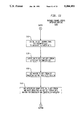
- FIG. 11 depicts a high level flowchart of Portable Channel Coding Interrupt Routine 1100. This routine performs channel coding of 147-bit informational bit streams that are to be transmitted as 164-bit TDMA bursts.
- routine 1100 upon entry into routine 1100, execution first proceeds to block 1110 which, when executed, divides a 147-bit informational bit stream by g(x) to calculate 14 corresponding parity bits. Thereafter, execution proceeds to block 1120 which, when executed, inserts these parity bits into this bit stream after the last one of the 147 information bits thereby forming a 161-bit codeword. Once this occurs, block 1130 is executed to add marker bits, specifically the first set thereof, to this codeword by inverting the values of the first and 161st bits in this bit stream.
- execution proceeds to block 1140 which inserts three appropriate dummy bits into this bit stream prior to the first informational bit and writes the resulting 164-bit bit stream for a new TDMA burst into RAM memory 960 for subsequent DMA transfer to the modulator situated within modulator/demodulator 975 (see FIG. 9).
- block 1140 is fully executed, then, as shown in FIG. 11, execution exits from routine 1100 and appropriately returns to a calling program or routine.
- FIGS. 12A and 12B collectively depict a high level flowchart of Portable Synchronization and Error Detection Interrupt Routine 1200; the correct alignment of the drawing sheets for these figures is shown in FIG. 12. This routine performs synchronization and error detection on received TDM words.
- routine 1200 execution first proceeds to block 1205.
- This block when executed, reads a 161-bits of information and parity from RAM 960 (see FIG. 9) for the word in the currently received TDM packet.
- block 1210 executes to add marker bits, specifically the second set thereof, to this word by inverting the first and 161st bits in this word.
- block 1215 which circularly rotates the 161 bits in the currently received, now marked, word to the left by 7 bit positions. After this rotation is complete, execution proceeds to block 1220 which divides the resulting 161 bits by polynomial g(x) and reads a resulting timing syndrome value.
- decision block 1225 This decision block determines if the timing syndrome value equals zero. If this syndrome value is zero, then no errors, either synchronization or erroneous bit(s), have occurred in the received word. Accordingly, decision block 1230 passes routes execution, via YES path 1229, to block 1230 which, when executed, sets the value of a software Error Flag to "zero". Execution then exits from routine 1200 and appropriately returns to a calling program or routine.
- decision block 1225 routes execution, via NO path 1227, to decision block 1235.
- This latter decision block determines whether this timing syndrome value matches any of the pre-defined values for bit slippages occurring between ⁇ 6 bits inclusive, i.e. those syndrome values shown in table 610 in FIG. 6. In part, this matching can simply be effected by counting the bit spacings that occur between delimiting marker ("1") bits in the timing syndrome. In the event a match was not found, thereby indicating excessive slippage or bit errors have occurred in the currently received word, then decision block routes execution, as shown in FIGS.
- Block 1240 which, when executed, sets the software Error Flag to "one" to signify that this word has errors and should be subsequently ignored. Execution then exits from routine 1200 and appropriately returns to a calling program or routine. By ignoring this erroneous word, the portable essentially “flywheels" using the previous synchronized substantially error-free codeword until the next successive synchronized substantially error-free codeword subsequently occurs. If, however, the non-zero timing syndrome value matches one of the pre-defined patterns, then decision block 1235 routes execution, via YES path 1239, to block 1245. Block 1245 determines the synch estimation (timing offset) value through table 610 shown in FIG. 6 for the current timing syndrome value.
- This block when executed, offsets the timing of the currently received 161-bit word by the value of the synch estimation by appropriately programming multiplexer 1035 located within multiplexed g(x) divider circuit 1000 shown in FIG. 10. Once the offset has been programmed into the multiplexer, execution proceeds, as shown in FIGS. 12A and 12B, to block 1255 which removes the marker bits, specifically the first set thereof, from this word by inverting the first and 161st bits of this word so as to form an unmarked word.
- the resulting error syndrome produced by this divider is then read.
- decision block 1265 routes execution, via NO path 1269, to block 1275.
- Block 1275 when executed, sets the value of the software Error Flag to "one" to signify that this word is erroneous and should be subsequently ignored.
- decision block 1265 routes execution, via YES path 1267, to block 1270 which sets the software Error Flag to "zero" to indicate that the unmarked word is a synchronized and substantially error-free codeword and should be subsequently used.
- the falsing rate using this code on this channel should be on the order of 2 -6 to 2 -7 or approximately 1 out of every 100 blocks.
- the resulting falsing rate will be on the order of approximately 2 -11 (approximately 7 ⁇ 2 -14 ), or approximately 1 out of every 1500 blocks, resulting in a three bit degradation in the falsing rate capability provided by the code if it was used only for error detection.
- our inventive technique jointly provides both synchronization and error detection in a much more implementationally efficient and cost effective manner than would use of separate error detection and synchronization processes such as that taught in the art, though at a cost, which is readily tolerable in speech transmission, of a slightly degraded falsing rate than that which would otherwise result if these separate processes were to be employed.
Abstract
Description
g(x) =x.sup.14 +x.sup.11 +x.sup.4 +x.sup.3 +x.sup.2 +1 (1)
Claims (38)
Priority Applications (1)
| Application Number | Priority Date | Filing Date | Title |
|---|---|---|---|
| US07/404,946 US5084891A (en) | 1989-09-08 | 1989-09-08 | Technique for jointly performing bit synchronization and error detection in a TDM/TDMA system |
Applications Claiming Priority (1)
| Application Number | Priority Date | Filing Date | Title |
|---|---|---|---|
| US07/404,946 US5084891A (en) | 1989-09-08 | 1989-09-08 | Technique for jointly performing bit synchronization and error detection in a TDM/TDMA system |
Publications (1)
| Publication Number | Publication Date |
|---|---|
| US5084891A true US5084891A (en) | 1992-01-28 |
Family
ID=23601675
Family Applications (1)
| Application Number | Title | Priority Date | Filing Date |
|---|---|---|---|
| US07/404,946 Expired - Lifetime US5084891A (en) | 1989-09-08 | 1989-09-08 | Technique for jointly performing bit synchronization and error detection in a TDM/TDMA system |
Country Status (1)
| Country | Link |
|---|---|
| US (1) | US5084891A (en) |
Cited By (105)
| Publication number | Priority date | Publication date | Assignee | Title |
|---|---|---|---|---|
| US5212690A (en) * | 1990-08-29 | 1993-05-18 | Bts Broadcast Television Systems Gmbh | Method of synchronizing digital data by comparing to a reference word to determine bit errors |
| WO1993010642A1 (en) * | 1991-11-19 | 1993-05-27 | Scientific-Atlanta, Inc. | Methods and apparatus for communicating program data signals via a remote control unit |
| US5226045A (en) * | 1992-05-07 | 1993-07-06 | Bell Communications Research, Inc. | Method and apparatus for autonomous selective routing during radio access in TDMA portable radio systems |
| US5323447A (en) * | 1991-11-01 | 1994-06-21 | At&T Bell Laboratories | Apparatus and method for modifying a frequency hopping sequence of a cordless telephone operating in a frequency hopping system |
| US5333175A (en) * | 1993-01-28 | 1994-07-26 | Bell Communications Research, Inc. | Method and apparatus for dynamic power control in TDMA portable radio systems |
| US5361258A (en) * | 1993-10-22 | 1994-11-01 | Bell Communications Research, Inc. | Beacon detection system for sharing spectrum between wireless communications systems and fixed microwave systems |
| US5363375A (en) * | 1993-07-30 | 1994-11-08 | Bell Communications Research, Inc. | Method and apparatus for synchronizing timing among radio ports in wireless communications systems using hierarchical scheme |
| US5363376A (en) * | 1993-07-30 | 1994-11-08 | Bell Communications Research, Inc. | Method and apparatus for synchronizing timing among radio ports in wireless communications systems |
| US5388126A (en) * | 1992-12-21 | 1995-02-07 | Rypinski; Chandos A. | Baseband signal processor for a microwave radio receiver |
| US5410588A (en) * | 1991-04-03 | 1995-04-25 | Kabushiki Kaisha Toshiba | Mobile radio communications system having a supervising radio transmitting station for transmitting a reference synchronizing signal to a first and second base stations via a radio link |
| US5412658A (en) * | 1993-10-22 | 1995-05-02 | Bell Communications Research, Inc. | Beacon detection method and apparatus for sharing spectrum between wireless communications systems and fixed microwave systems |
| US5414830A (en) * | 1990-07-11 | 1995-05-09 | Bull, S.A. | Apparatus for serialization and deserialization of data, and resultant system for digital transmission of serial data |
| US5426641A (en) * | 1994-01-28 | 1995-06-20 | Bell Communications Research, Inc. | Adaptive class AB amplifier for TDMA wireless communications systems |
| US5430789A (en) * | 1992-11-04 | 1995-07-04 | Nec Corporation | Cellular mobile base station apparatus for serving a first and second cell zones |
| US5475677A (en) * | 1994-12-29 | 1995-12-12 | Bell Communications Research Inc. | Compatible licensed and unlicensed band portable handset unit for TDMA wireless communications system |
| US5475696A (en) * | 1990-10-30 | 1995-12-12 | Fujitsu Limited | Remote alarm transfer method and system |
| EP0689295A1 (en) * | 1994-06-14 | 1995-12-27 | Koninklijke KPN N.V. | A system comprising an encoder for coding words in a cyclic manner and comprising a decoder for decoding words which have been coded in a cyclic manner and also an encoder, and also a decoder, and also a method, and also an object |
| US5490148A (en) * | 1993-12-15 | 1996-02-06 | Motorola, Inc. | Bit error rate estimator |
| US5491719A (en) * | 1993-07-02 | 1996-02-13 | Telefonaktiebolaget Lm Ericsson | System for handling data errors on a cellular communications system PCM link |
| US5500620A (en) * | 1993-04-02 | 1996-03-19 | Northern Telecom Limited | Timing recovery for digital demodulation |
| FR2733655A1 (en) * | 1995-04-28 | 1996-10-31 | Ind Tech Res Inst | METHOD AND SYSTEM FOR ACQUIRING ARRAY DRIVING FOR TIME-DIVISION MULTIPLE ACCESS WIRELESS SYSTEMS |
| US5574750A (en) * | 1993-09-14 | 1996-11-12 | Pacific Communication Sciences, Inc. | Methods and apparatus for detecting a cellular digital packet data (CDPD) carrier |
| US5586150A (en) * | 1993-11-24 | 1996-12-17 | Rajupandaram K. Balasubramaniam | Method and apparatus for symbol synchronization in multi-level digital FM radio |
| WO1997021285A1 (en) * | 1995-12-05 | 1997-06-12 | Stanford Telecommunications, Inc. | Network protocol for wireless broadband isdn using atm |
| US5651015A (en) * | 1995-03-02 | 1997-07-22 | Northern Telecom Limited | Apparatus and method for synchronization and error detection of received digital data bursts in a TDM/TDMA system |
| US5689568A (en) * | 1995-06-29 | 1997-11-18 | Hughes Electronics | Medium access control for a mobile satellite system |
| US5699389A (en) * | 1995-09-28 | 1997-12-16 | Motorola, Inc. | Oversampling correlator with virtual clock phase for a telecommunications device |
| US5715278A (en) * | 1993-05-11 | 1998-02-03 | Ericsson Inc. | Standby power saving in mobile phones |
| US5745510A (en) * | 1994-06-29 | 1998-04-28 | Korea Telecommunications Authority | System for detecting frame/burst synchronization and channel error using cyclic code |
| US5757810A (en) * | 1995-11-24 | 1998-05-26 | Telefonaktiebolaget Lm Ericsson | Transmission link supervision in radiocommunication systems |
| US5793957A (en) * | 1993-05-25 | 1998-08-11 | Elonex I.P. Holdings, Ltd. | Satellite digital assistant and host/satellite computer system wherein coupling the host and the satellite by a host interface communication system results in digital communication and synchronization of files |
| US5822339A (en) * | 1996-05-30 | 1998-10-13 | Rockwell International | Data decoder and method to correct inversions or phase ambiguity for M-ary transmitted data |
| US5832002A (en) * | 1991-09-20 | 1998-11-03 | Abb Signal Ab | Method for coding and decoding a digital message |
| US5832031A (en) * | 1995-08-18 | 1998-11-03 | Hughes Electronics Corporation | Method and apparatus for performing cyclic redundancy check synchronization |
| US5854808A (en) * | 1993-09-14 | 1998-12-29 | Pacific Communication Sciences | Methods and apparatus for detecting the presence of a prescribed signal in a channel of a communications system |
| US5878062A (en) * | 1997-01-24 | 1999-03-02 | Nokia Telecommunications Oy | Data transfer method and a cellular radio system |
| US5933468A (en) * | 1997-03-06 | 1999-08-03 | Telefonaktiebolaget L M Ericsson (Publ) | Continuous synchronization adjustment in a telecommunications system |
| US5991632A (en) * | 1997-04-04 | 1999-11-23 | Casio Phonemate, Inc. | Cordless telephone and method of synchronization for secure, high-speed, high-volume data transfer |
| US6101465A (en) * | 1997-06-12 | 2000-08-08 | Advanced Micro Devices, Inc. | System and method for bit interleaving of full-rate speech data |
| US6122525A (en) * | 1995-08-07 | 2000-09-19 | Motorola, Inc. | International mobile station identification method and signaling system for cellular radiotelephones and systems |
| US6124696A (en) * | 1999-07-14 | 2000-09-26 | Lexmark International, Inc. | Programmable stepper motor controller and method therefor |
| US6195783B1 (en) * | 1995-03-27 | 2001-02-27 | Blaupunkt-Werke Gmbh | Process and apparatus for synchronizing the block counter in an RDS radio data receiver |
| US6275966B1 (en) * | 1998-06-03 | 2001-08-14 | Ericsson, Inc. | Error detection for radio transmission including logically combined pseudo-random numbers and related transmitters, receivers, and methods |
| US6298225B1 (en) * | 1996-01-31 | 2001-10-02 | Nokia Mobile Phones Limited | Radio telephones and method of operation |
| US20010033188A1 (en) * | 2000-03-14 | 2001-10-25 | Edward Aung | Clock data recovery circuitry associated with programmable logic device circuitry |
| US20020022463A1 (en) * | 2000-04-06 | 2002-02-21 | Shinichi Mori | Apparatus and method for acquisition of communication quality |
| US20020034297A1 (en) * | 1996-04-25 | 2002-03-21 | Rhoads Geoffrey B. | Wireless methods and devices employing steganography |
| US20020041647A1 (en) * | 2000-10-02 | 2002-04-11 | Shih-Chuan Lin | Device and method for burst synchronization and error detection |
| US6378103B1 (en) * | 1998-05-19 | 2002-04-23 | Samsung Electronics Co., Ltd. | Apparatus and method for error correction in optical disk system |
| US6427219B1 (en) * | 1998-06-24 | 2002-07-30 | Conexant Systems, Inc. | Method and apparatus for detecting and correcting errors using cyclic redundancy check |
| US6618395B1 (en) * | 1999-05-27 | 2003-09-09 | 3Com Corporation | Physical coding sub-layer for transmission of data over multi-channel media |
| US20030212930A1 (en) * | 2000-03-14 | 2003-11-13 | Altera Corporation | Clock data recovery circuitry associated with programmable logic device circuitry |
| US6742154B1 (en) * | 2000-05-25 | 2004-05-25 | Ciena Corporation | Forward error correction codes for digital optical network optimization |
| US20040131085A1 (en) * | 2002-09-25 | 2004-07-08 | Stmicroelectronics S.R.L. | Process and devices for transmitting digital signals over buses and computer program product therefore |
| US20040153927A1 (en) * | 2002-09-25 | 2004-08-05 | Stmicroelectronics S.R.L. | Process and devices for transmitting digital signals over buses and computer program product therefore |
| US20040161086A1 (en) * | 1998-12-11 | 2004-08-19 | Securelogix Corporation | Telephony security system |
| US20040193994A1 (en) * | 2003-03-28 | 2004-09-30 | Pulakesh Roy | Error word generation with multiple element input |
| US20040196838A1 (en) * | 1999-01-15 | 2004-10-07 | Zadikian Haig Michael | Configurable network router |
| US20040199819A1 (en) * | 2001-08-10 | 2004-10-07 | Jorg Dauerer | Method for fast and local error correction in the event of the failure of individual physical corrections in bundled communication connections and communication system device for carrying out the method |
| US6810501B1 (en) * | 2001-01-03 | 2004-10-26 | Juniper Networks, Inc. | Single cycle cyclic redundancy checker/generator |
| US20040218742A1 (en) * | 2001-07-23 | 2004-11-04 | Greg Schmid | Encapsulation, compression, and encryption of PCM data |
| US20040234056A1 (en) * | 2001-07-17 | 2004-11-25 | Securelogix Corporation | Telephony security system |
| US20050025302A1 (en) * | 2002-07-23 | 2005-02-03 | Greg Schmid | Virtual private switched telecommunications network |
| US20050047570A1 (en) * | 2003-08-27 | 2005-03-03 | Greg Schmid | Virtual private switched telecommunications network |
| US6982974B1 (en) | 1999-01-15 | 2006-01-03 | Cisco Technology, Inc. | Method and apparatus for a rearrangeably non-blocking switching matrix |
| US20060018176A1 (en) * | 2004-07-26 | 2006-01-26 | Integrated Device Technology, Inc. | Mark/re-read and mark/re-write operations in a multi-queue first-in first-out memory system |
| US20060018177A1 (en) * | 2004-07-26 | 2006-01-26 | Integrated Device Technology, Inc. | Multiple counters to relieve flag restriction in a multi-queue first-in first-out memory system |
| US20060020761A1 (en) * | 2004-07-26 | 2006-01-26 | Integrated Device Technology, Inc. | Partial packet read/write and data filtering in a multi-queue first-in first-out memory system |
| US20060020742A1 (en) * | 2004-07-26 | 2006-01-26 | Integrated Device Technology, Inc. | Status bus accessing only available quadrants during loop mode operation in a multi-queue first-in first-out memory system |
| US20060017497A1 (en) * | 2004-07-26 | 2006-01-26 | Integrated Device Technology, Inc. | Self-timed multiple blanking for noise suppression during flag generation in a multi-queue first-in first-out memory system |
| US20060020741A1 (en) * | 2004-07-26 | 2006-01-26 | Integrated Device Technology, Inc. | Synchronization of active flag and status bus flags in a multi-queue first-in first-out memory system |
| US20060018170A1 (en) * | 2004-07-26 | 2006-01-26 | Integrated Device Technology, Inc. | Interleaving memory blocks to relieve timing bottleneck in a multi-queue first-in first-out memory system |
| US20060153163A1 (en) * | 2005-01-07 | 2006-07-13 | At&T Corp. | System and method for modifying speech playout to compensate for transmission delay jitter in a Voice over Internet protocol (VoIP) network |
| US20060240854A1 (en) * | 2003-02-11 | 2006-10-26 | Ju-Ho Lee | Sychronization method for terminal-to-terminal direct communication in time division duplex mobile communication system |
| US20070050660A1 (en) * | 2005-08-29 | 2007-03-01 | Searete Llc, A Limited Liability Corporation Of The State Of Delaware | Handling processor computational errors |
| US20070050608A1 (en) * | 2005-08-29 | 2007-03-01 | Searete Llc, A Limited Liability Corporatin Of The State Of Delaware | Hardware-generated and historically-based execution optimization |
| US20070050558A1 (en) * | 2005-08-29 | 2007-03-01 | Bran Ferren | Multiprocessor resource optimization |
| US20070050557A1 (en) * | 2005-08-29 | 2007-03-01 | Searete Llc, A Limited Liability Corporation Of The State Of Delaware | Multiprocessor resource optimization |
| US20070050605A1 (en) * | 2005-08-29 | 2007-03-01 | Bran Ferren | Freeze-dried ghost pages |
| US20070050581A1 (en) * | 2005-08-29 | 2007-03-01 | Searete Llc, A Limited Liability Corporation Of The State Of Delaware | Power sparing synchronous apparatus |
| US20070050672A1 (en) * | 2005-08-29 | 2007-03-01 | Searete Llc, A Limited Liability Corporation Of The State Of Delaware | Power consumption management |
| US20070050775A1 (en) * | 2005-08-29 | 2007-03-01 | Searete Llc, A Limited Liability Corporation Of The State Of Delaware | Processor resource management |
| US20070050556A1 (en) * | 2005-08-29 | 2007-03-01 | Searete Llc, A Limited Liability Corporation Of The State Of Delaware | Multiprocessor resource optimization |
| US20070050609A1 (en) * | 2005-08-29 | 2007-03-01 | Searete Llc | Cross-architecture execution optimization |
| US20070050776A1 (en) * | 2005-08-29 | 2007-03-01 | Searete Llc, A Limited Liability Corporation Of The State Of Delaware | Predictive processor resource management |
| US20070055848A1 (en) * | 2005-08-29 | 2007-03-08 | Searete Llc, A Limited Liability Corporation Of The State Of Delaware | Processor resource management |
| US20070067611A1 (en) * | 2005-08-29 | 2007-03-22 | Bran Ferren | Processor resource management |
| US20070074173A1 (en) * | 2005-08-29 | 2007-03-29 | Bran Ferren | Cross-architecture optimization |
| US20070086327A1 (en) * | 1999-02-08 | 2007-04-19 | Langley John B | Frequency offset differential pulse position modulation |
| US20070127448A1 (en) * | 2000-11-10 | 2007-06-07 | Buntin David L | Telephony security system |
| US20070189533A1 (en) * | 1996-04-25 | 2007-08-16 | Rhoads Geoffrey B | Wireless Methods And Devices Employing Steganography |
| US7293090B1 (en) | 1999-01-15 | 2007-11-06 | Cisco Technology, Inc. | Resource management protocol for a configurable network router |
| US20080082896A1 (en) * | 2006-08-25 | 2008-04-03 | Broadcom Corporation | Burst error correction with offset for correction vector based on fire code |
| US7392354B1 (en) | 2005-01-10 | 2008-06-24 | Integrated Device Technology, Inc. | Multi-queue FIFO memory devices that support a backed-off standard mode of operation and methods of operating same |
| US7447812B1 (en) | 2004-03-23 | 2008-11-04 | Integrated Device Technology, Inc. | Multi-queue FIFO memory devices that support flow-through of write and read counter updates using multi-port flag counter register files |
| US20080310299A1 (en) * | 1999-01-15 | 2008-12-18 | Saleh Ali N | Virtual Path Restoration Scheme Using Fast Dynamic Mesh Restoration in an Optical Network |
| US20090132853A1 (en) * | 2005-08-29 | 2009-05-21 | Searete Llc, A Limited Liability Corporation Of The State Of Delaware | Hardware-error tolerant computing |
| US20090150713A1 (en) * | 2005-08-29 | 2009-06-11 | William Henry Mangione-Smith | Multi-voltage synchronous systems |
| US7577188B1 (en) * | 2001-09-13 | 2009-08-18 | Cisco Technology, Inc. | Physical layer and MAC enhancements using complex sequences on a wireless channel |
| US20090228759A1 (en) * | 2002-01-21 | 2009-09-10 | Koninklijke Philips Electronics, N.V. | Method of encoding and decodoing |
| US20100195835A1 (en) * | 2009-02-05 | 2010-08-05 | D.E. Shaw Research, Llc | Link and physical coding sub-layer protocols |
| WO2010146472A3 (en) * | 2009-06-16 | 2011-04-07 | Alcatel Lucent | Maintaining time-division multiplexing over pseudowire connections during network outages |
| US20160081048A1 (en) * | 2001-02-01 | 2016-03-17 | James A. Proctor, Jr. | Use of correlation combination to achieve channel detection |
| US20180007078A1 (en) * | 2016-07-01 | 2018-01-04 | Texas Instruments Incorporated | Relay-attack resistant communications |
| US11416438B2 (en) * | 2017-05-19 | 2022-08-16 | Seiko Epson Corporation | Circuit device, electronic device, cable harness, and data transfer method |
Citations (2)
| Publication number | Priority date | Publication date | Assignee | Title |
|---|---|---|---|---|
| US3550082A (en) * | 1966-03-17 | 1970-12-22 | Bell Telephone Labor Inc | Automatic synchronization recovery techniques for nonbinary cyclic codes |
| US3571794A (en) * | 1967-09-27 | 1971-03-23 | Bell Telephone Labor Inc | Automatic synchronization recovery for data systems utilizing burst-error-correcting cyclic codes |
-
1989
- 1989-09-08 US US07/404,946 patent/US5084891A/en not_active Expired - Lifetime
Patent Citations (2)
| Publication number | Priority date | Publication date | Assignee | Title |
|---|---|---|---|---|
| US3550082A (en) * | 1966-03-17 | 1970-12-22 | Bell Telephone Labor Inc | Automatic synchronization recovery techniques for nonbinary cyclic codes |
| US3571794A (en) * | 1967-09-27 | 1971-03-23 | Bell Telephone Labor Inc | Automatic synchronization recovery for data systems utilizing burst-error-correcting cyclic codes |
Non-Patent Citations (18)
| Title |
|---|
| Cox, "Portable Digital Radio Communications--An Approach to Tetherless Access", IEEE Communications Magazine, vol. 27, No. 7, Jul. 1989, pp. 30-40. |
| Cox, "Universal Digital Portable Radio Communications", Proceedings of the IEEE, vol. 75, No. 4, Apr. 1987, pp. 436-476. |
| Cox, Portable Digital Radio Communications An Approach to Tetherless Access , IEEE Communications Magazine, vol. 27, No. 7, Jul. 1989, pp. 30 40. * |
| Cox, Universal Digital Portable Radio Communications , Proceedings of the IEEE, vol. 75, No. 4, Apr. 1987, pp. 436 476. * |
| Peterson et al, Error Correcting Codes (Second Edition) 1972, The MIT Press, Cambridge, Mass.) specifically section 7.2 Multiplication and Division of Polynomials on pp. 171 178, section 8.8, Error Detection with Cyclic Codes on pp. 228 230, and chapter 12 Synchronization of Block Codes on pp. 374 391 thereof. * |
| Peterson et al, Error-Correcting Codes (Second Edition) ©1972, The MIT Press, Cambridge, Mass.) specifically section 7.2 "Multiplication and Division of Polynomials" on pp. 171-178, section 8.8, Error Detection with Cyclic Codes on pp. 228-230, and chapter 12 Synchronization of Block Codes on pp. 374-391 thereof. |
| Scholtz, "Frame Synchronization Techniques", IEEE Transactions on Communications, vol. COM-28, No. 8, Aug. 1980, pp. 1204-1213. |
| Scholtz, Frame Synchronization Techniques , IEEE Transactions on Communications, vol. COM 28, No. 8, Aug. 1980, pp. 1204 1213. * |
| Stiffler, Theory of Synchronous Communication ( 1971, Prentice Hall Pub. Co., Englewood Cliffs, N.J.) specifically chapter 14 Synchronizable Error Correcting Codes on pp. 453 511 thereof. * |
| Stiffler, Theory of Synchronous Communication (©1971, Prentice Hall Pub. Co., Englewood Cliffs, N.J.) specifically chapter 14 "Synchronizable Error-Correcting Codes" on pp. 453-511 thereof. |
| Tavares et al, "Further Results on the Synchronization of Binary Cyclic Codes", IEEE Transactions on Information Theory, Mar. 1970, pp. 238-241. |
| Tavares et al, "Synchronization of a Class of Codes Derived from Cyclic Codes", Information and Control, vol. 16, 1970, pp. 153-166. |
| Tavares et al, "Synchronization of Cyclic Codes in the Presence of Burst Errors", Information and Control, vol. 14, 1969, pp. 423-441. |
| Tavares et al, Further Results on the Synchronization of Binary Cyclic Codes , IEEE Transactions on Information Theory, Mar. 1970, pp. 238 241. * |
| Tavares et al, Synchronization of a Class of Codes Derived from Cyclic Codes , Information and Control, vol. 16, 1970, pp. 153 166. * |
| Tavares et al, Synchronization of Cyclic Codes in the Presence of Burst Errors , Information and Control, vol. 14, 1969, pp. 423 441. * |
| Tong, "Synchronization Recovery Techniques for Binary Cyclic Codes", The Bell System Technical Journal, Apr. 1966, pp. 561-596. |
| Tong, Synchronization Recovery Techniques for Binary Cyclic Codes , The Bell System Technical Journal, Apr. 1966, pp. 561 596. * |
Cited By (184)
| Publication number | Priority date | Publication date | Assignee | Title |
|---|---|---|---|---|
| US5414830A (en) * | 1990-07-11 | 1995-05-09 | Bull, S.A. | Apparatus for serialization and deserialization of data, and resultant system for digital transmission of serial data |
| US5212690A (en) * | 1990-08-29 | 1993-05-18 | Bts Broadcast Television Systems Gmbh | Method of synchronizing digital data by comparing to a reference word to determine bit errors |
| US5475696A (en) * | 1990-10-30 | 1995-12-12 | Fujitsu Limited | Remote alarm transfer method and system |
| US5410588A (en) * | 1991-04-03 | 1995-04-25 | Kabushiki Kaisha Toshiba | Mobile radio communications system having a supervising radio transmitting station for transmitting a reference synchronizing signal to a first and second base stations via a radio link |
| US5832002A (en) * | 1991-09-20 | 1998-11-03 | Abb Signal Ab | Method for coding and decoding a digital message |
| US5323447A (en) * | 1991-11-01 | 1994-06-21 | At&T Bell Laboratories | Apparatus and method for modifying a frequency hopping sequence of a cordless telephone operating in a frequency hopping system |
| WO1993010642A1 (en) * | 1991-11-19 | 1993-05-27 | Scientific-Atlanta, Inc. | Methods and apparatus for communicating program data signals via a remote control unit |
| US5226045A (en) * | 1992-05-07 | 1993-07-06 | Bell Communications Research, Inc. | Method and apparatus for autonomous selective routing during radio access in TDMA portable radio systems |
| US5430789A (en) * | 1992-11-04 | 1995-07-04 | Nec Corporation | Cellular mobile base station apparatus for serving a first and second cell zones |
| US5388126A (en) * | 1992-12-21 | 1995-02-07 | Rypinski; Chandos A. | Baseband signal processor for a microwave radio receiver |
| US5333175A (en) * | 1993-01-28 | 1994-07-26 | Bell Communications Research, Inc. | Method and apparatus for dynamic power control in TDMA portable radio systems |
| US5500620A (en) * | 1993-04-02 | 1996-03-19 | Northern Telecom Limited | Timing recovery for digital demodulation |
| US5715278A (en) * | 1993-05-11 | 1998-02-03 | Ericsson Inc. | Standby power saving in mobile phones |
| US5793957A (en) * | 1993-05-25 | 1998-08-11 | Elonex I.P. Holdings, Ltd. | Satellite digital assistant and host/satellite computer system wherein coupling the host and the satellite by a host interface communication system results in digital communication and synchronization of files |
| US5491719A (en) * | 1993-07-02 | 1996-02-13 | Telefonaktiebolaget Lm Ericsson | System for handling data errors on a cellular communications system PCM link |
| US5363375A (en) * | 1993-07-30 | 1994-11-08 | Bell Communications Research, Inc. | Method and apparatus for synchronizing timing among radio ports in wireless communications systems using hierarchical scheme |
| US5363376A (en) * | 1993-07-30 | 1994-11-08 | Bell Communications Research, Inc. | Method and apparatus for synchronizing timing among radio ports in wireless communications systems |
| US5719902A (en) * | 1993-09-14 | 1998-02-17 | Pacific Communication Sciences, Inc. | Methods and apparatus for detecting cellular digital packet data (CDPD) |
| US5854808A (en) * | 1993-09-14 | 1998-12-29 | Pacific Communication Sciences | Methods and apparatus for detecting the presence of a prescribed signal in a channel of a communications system |
| US5574750A (en) * | 1993-09-14 | 1996-11-12 | Pacific Communication Sciences, Inc. | Methods and apparatus for detecting a cellular digital packet data (CDPD) carrier |
| US5412658A (en) * | 1993-10-22 | 1995-05-02 | Bell Communications Research, Inc. | Beacon detection method and apparatus for sharing spectrum between wireless communications systems and fixed microwave systems |
| US5361258A (en) * | 1993-10-22 | 1994-11-01 | Bell Communications Research, Inc. | Beacon detection system for sharing spectrum between wireless communications systems and fixed microwave systems |
| US7522728B1 (en) * | 1993-11-18 | 2009-04-21 | Digimarc Corporation | Wireless methods and devices employing steganography |
| US5586150A (en) * | 1993-11-24 | 1996-12-17 | Rajupandaram K. Balasubramaniam | Method and apparatus for symbol synchronization in multi-level digital FM radio |
| US5490148A (en) * | 1993-12-15 | 1996-02-06 | Motorola, Inc. | Bit error rate estimator |
| US5426641A (en) * | 1994-01-28 | 1995-06-20 | Bell Communications Research, Inc. | Adaptive class AB amplifier for TDMA wireless communications systems |
| NL9400965A (en) * | 1994-06-14 | 1996-01-02 | Nederland Ptt | System comprising an encoder for cyclically encoding words and comprising a decoder for decoding cyclically encoded words, as well as an encoder and decoder, and a method for assigning a word encoded cyclically to an object and for detecting on a receiving side the word assigned to the object in a cyclically encoded word, as well as an object provided with a word encoded in a cyclical manner. |
| EP0689295A1 (en) * | 1994-06-14 | 1995-12-27 | Koninklijke KPN N.V. | A system comprising an encoder for coding words in a cyclic manner and comprising a decoder for decoding words which have been coded in a cyclic manner and also an encoder, and also a decoder, and also a method, and also an object |
| US5745510A (en) * | 1994-06-29 | 1998-04-28 | Korea Telecommunications Authority | System for detecting frame/burst synchronization and channel error using cyclic code |
| US5475677A (en) * | 1994-12-29 | 1995-12-12 | Bell Communications Research Inc. | Compatible licensed and unlicensed band portable handset unit for TDMA wireless communications system |
| US5651015A (en) * | 1995-03-02 | 1997-07-22 | Northern Telecom Limited | Apparatus and method for synchronization and error detection of received digital data bursts in a TDM/TDMA system |
| US6195783B1 (en) * | 1995-03-27 | 2001-02-27 | Blaupunkt-Werke Gmbh | Process and apparatus for synchronizing the block counter in an RDS radio data receiver |
| FR2733655A1 (en) * | 1995-04-28 | 1996-10-31 | Ind Tech Res Inst | METHOD AND SYSTEM FOR ACQUIRING ARRAY DRIVING FOR TIME-DIVISION MULTIPLE ACCESS WIRELESS SYSTEMS |
| US5689568A (en) * | 1995-06-29 | 1997-11-18 | Hughes Electronics | Medium access control for a mobile satellite system |
| US6122525A (en) * | 1995-08-07 | 2000-09-19 | Motorola, Inc. | International mobile station identification method and signaling system for cellular radiotelephones and systems |
| US5832031A (en) * | 1995-08-18 | 1998-11-03 | Hughes Electronics Corporation | Method and apparatus for performing cyclic redundancy check synchronization |
| US5699389A (en) * | 1995-09-28 | 1997-12-16 | Motorola, Inc. | Oversampling correlator with virtual clock phase for a telecommunications device |
| US5757810A (en) * | 1995-11-24 | 1998-05-26 | Telefonaktiebolaget Lm Ericsson | Transmission link supervision in radiocommunication systems |
| AU709237B2 (en) * | 1995-12-05 | 1999-08-26 | Stanford Telecommunications, Inc. | Network protocol for wireless broadband ISDN using ATM |
| WO1997021285A1 (en) * | 1995-12-05 | 1997-06-12 | Stanford Telecommunications, Inc. | Network protocol for wireless broadband isdn using atm |
| US5751702A (en) * | 1995-12-05 | 1998-05-12 | Stanford Telecommunications, Inc. | Network protocol for wireless broadband ISDN using ATM |
| US6298225B1 (en) * | 1996-01-31 | 2001-10-02 | Nokia Mobile Phones Limited | Radio telephones and method of operation |
| US8027663B2 (en) | 1996-04-25 | 2011-09-27 | Digimarc Corporation | Wireless methods and devices employing steganography |
| US20080125083A1 (en) * | 1996-04-25 | 2008-05-29 | Rhoads Geoffrey B | Wireless Methods and Devices Employing Steganography |
| US7362781B2 (en) | 1996-04-25 | 2008-04-22 | Digimarc Corporation | Wireless methods and devices employing steganography |
| US7715446B2 (en) | 1996-04-25 | 2010-05-11 | Digimarc Corporation | Wireless methods and devices employing plural-bit data derived from audio information |
| US20070189533A1 (en) * | 1996-04-25 | 2007-08-16 | Rhoads Geoffrey B | Wireless Methods And Devices Employing Steganography |
| US20100296526A1 (en) * | 1996-04-25 | 2010-11-25 | Rhoads Geoffrey B | Wireless Methods and Devices Employing Plural-Bit Data Derived from Audio Information |
| US8369363B2 (en) | 1996-04-25 | 2013-02-05 | Digimarc Corporation | Wireless methods and devices employing plural-bit data derived from audio information |
| US20020034297A1 (en) * | 1996-04-25 | 2002-03-21 | Rhoads Geoffrey B. | Wireless methods and devices employing steganography |
| US5822339A (en) * | 1996-05-30 | 1998-10-13 | Rockwell International | Data decoder and method to correct inversions or phase ambiguity for M-ary transmitted data |
| US5878062A (en) * | 1997-01-24 | 1999-03-02 | Nokia Telecommunications Oy | Data transfer method and a cellular radio system |
| US5933468A (en) * | 1997-03-06 | 1999-08-03 | Telefonaktiebolaget L M Ericsson (Publ) | Continuous synchronization adjustment in a telecommunications system |
| US5991632A (en) * | 1997-04-04 | 1999-11-23 | Casio Phonemate, Inc. | Cordless telephone and method of synchronization for secure, high-speed, high-volume data transfer |
| US6324504B1 (en) * | 1997-06-12 | 2001-11-27 | Legerity, Inc. | System and method for bit interleaving of full-rate speech data |
| US6101465A (en) * | 1997-06-12 | 2000-08-08 | Advanced Micro Devices, Inc. | System and method for bit interleaving of full-rate speech data |
| US6378103B1 (en) * | 1998-05-19 | 2002-04-23 | Samsung Electronics Co., Ltd. | Apparatus and method for error correction in optical disk system |
| US6275966B1 (en) * | 1998-06-03 | 2001-08-14 | Ericsson, Inc. | Error detection for radio transmission including logically combined pseudo-random numbers and related transmitters, receivers, and methods |
| US6427219B1 (en) * | 1998-06-24 | 2002-07-30 | Conexant Systems, Inc. | Method and apparatus for detecting and correcting errors using cyclic redundancy check |
| US7133511B2 (en) | 1998-12-11 | 2006-11-07 | Securelogix Corporation | Telephony security system |
| US20040161086A1 (en) * | 1998-12-11 | 2004-08-19 | Securelogix Corporation | Telephony security system |
| US7933266B2 (en) | 1999-01-15 | 2011-04-26 | Cisco Technology, Inc. | Configurable network router |
| US20080310299A1 (en) * | 1999-01-15 | 2008-12-18 | Saleh Ali N | Virtual Path Restoration Scheme Using Fast Dynamic Mesh Restoration in an Optical Network |
| US7293090B1 (en) | 1999-01-15 | 2007-11-06 | Cisco Technology, Inc. | Resource management protocol for a configurable network router |
| US20040196838A1 (en) * | 1999-01-15 | 2004-10-07 | Zadikian Haig Michael | Configurable network router |
| US6982974B1 (en) | 1999-01-15 | 2006-01-03 | Cisco Technology, Inc. | Method and apparatus for a rearrangeably non-blocking switching matrix |
| US8537836B2 (en) | 1999-01-15 | 2013-09-17 | Cisco Technology, Inc. | Virtual path restoration scheme using fast dynamic mesh restoration in an optical network |
| US7626918B2 (en) | 1999-02-08 | 2009-12-01 | Langley John B | Frequency offset differential pulse position modulation |
| US7706247B2 (en) | 1999-02-08 | 2010-04-27 | Langley John B | Frequency offset differential pulse position modulation |
| US7609712B2 (en) | 1999-02-08 | 2009-10-27 | Langley John B | Frequency offset differential pulse position modulation |
| US20070110149A1 (en) * | 1999-02-08 | 2007-05-17 | Langley John B | Frequency offset differential pulse position modulation |
| US20070086326A1 (en) * | 1999-02-08 | 2007-04-19 | Langley John B | Frequency offset differential pulse position modulation |
| US20070086327A1 (en) * | 1999-02-08 | 2007-04-19 | Langley John B | Frequency offset differential pulse position modulation |
| US7564863B2 (en) * | 1999-02-08 | 2009-07-21 | Langley John B | Frequency offset differential pulse position modulation |
| US20040022238A1 (en) * | 1999-05-27 | 2004-02-05 | Myles Kimmitt | Physical coding sub-layer for transmission of data over multi-channel media |
| US6618395B1 (en) * | 1999-05-27 | 2003-09-09 | 3Com Corporation | Physical coding sub-layer for transmission of data over multi-channel media |
| US6124696A (en) * | 1999-07-14 | 2000-09-26 | Lexmark International, Inc. | Programmable stepper motor controller and method therefor |
| US20030212930A1 (en) * | 2000-03-14 | 2003-11-13 | Altera Corporation | Clock data recovery circuitry associated with programmable logic device circuitry |
| US20080031385A1 (en) * | 2000-03-14 | 2008-02-07 | Altera Corporation | Clock data recovery circuitry associated with programmable logic device circuitry |
| US20010033188A1 (en) * | 2000-03-14 | 2001-10-25 | Edward Aung | Clock data recovery circuitry associated with programmable logic device circuitry |
| US7684532B2 (en) | 2000-03-14 | 2010-03-23 | Altera Corporation | Clock data recovery circuitry associated with programmable logic device circuitry |
| US7333570B2 (en) | 2000-03-14 | 2008-02-19 | Altera Corporation | Clock data recovery circuitry associated with programmable logic device circuitry |
| US7227918B2 (en) * | 2000-03-14 | 2007-06-05 | Altera Corporation | Clock data recovery circuitry associated with programmable logic device circuitry |
| US6968197B2 (en) * | 2000-04-06 | 2005-11-22 | Ntt Docomo, Inc. | Apparatus and method for acquisition of communication quality |
| US20020022463A1 (en) * | 2000-04-06 | 2002-02-21 | Shinichi Mori | Apparatus and method for acquisition of communication quality |
| US6742154B1 (en) * | 2000-05-25 | 2004-05-25 | Ciena Corporation | Forward error correction codes for digital optical network optimization |
| US20020041647A1 (en) * | 2000-10-02 | 2002-04-11 | Shih-Chuan Lin | Device and method for burst synchronization and error detection |
| US6763078B2 (en) * | 2000-10-02 | 2004-07-13 | Syncomm Technology Corp. | Device and method for burst synchronization and error detection |
| US20070127448A1 (en) * | 2000-11-10 | 2007-06-07 | Buntin David L | Telephony security system |
| US8150013B2 (en) | 2000-11-10 | 2012-04-03 | Securelogix Corporation | Telephony security system |
| US6810501B1 (en) * | 2001-01-03 | 2004-10-26 | Juniper Networks, Inc. | Single cycle cyclic redundancy checker/generator |
| US10064144B2 (en) * | 2001-02-01 | 2018-08-28 | Intel Corporation | Use of correlation combination to achieve channel detection |
| US20160081048A1 (en) * | 2001-02-01 | 2016-03-17 | James A. Proctor, Jr. | Use of correlation combination to achieve channel detection |
| US7440558B2 (en) | 2001-07-17 | 2008-10-21 | Securelogix Corporation | Telephony security system |
| US20040234056A1 (en) * | 2001-07-17 | 2004-11-25 | Securelogix Corporation | Telephony security system |
| US20040218742A1 (en) * | 2001-07-23 | 2004-11-04 | Greg Schmid | Encapsulation, compression, and encryption of PCM data |
| US7231027B2 (en) | 2001-07-23 | 2007-06-12 | Securelogix Corporation | Encapsulation, compression, and encryption of PCM data |
| US20040199819A1 (en) * | 2001-08-10 | 2004-10-07 | Jorg Dauerer | Method for fast and local error correction in the event of the failure of individual physical corrections in bundled communication connections and communication system device for carrying out the method |
| US7577188B1 (en) * | 2001-09-13 | 2009-08-18 | Cisco Technology, Inc. | Physical layer and MAC enhancements using complex sequences on a wireless channel |
| US9183080B2 (en) | 2002-01-21 | 2015-11-10 | Koninklijke Philips N.V. | Device for encoding and decoding using smaller block of symbols |
| US20090228759A1 (en) * | 2002-01-21 | 2009-09-10 | Koninklijke Philips Electronics, N.V. | Method of encoding and decodoing |
| US8683300B2 (en) * | 2002-01-21 | 2014-03-25 | Koninklijke Philips N.V. | Method of encoding and decoding |
| US20050025302A1 (en) * | 2002-07-23 | 2005-02-03 | Greg Schmid | Virtual private switched telecommunications network |
| US20080211701A1 (en) * | 2002-09-25 | 2008-09-04 | Stmicroelectronics S.R.I. | Process and devices for transmitting digital signals over buses and computer program product therefore |
| US20040131085A1 (en) * | 2002-09-25 | 2004-07-08 | Stmicroelectronics S.R.L. | Process and devices for transmitting digital signals over buses and computer program product therefore |
| US7372916B2 (en) | 2002-09-25 | 2008-05-13 | Stmicroelectronics S.R.L | Process and devices for transmitting digital signals over buses and computer program product therefore |
| US6943706B2 (en) * | 2002-09-25 | 2005-09-13 | Stmicroelectronics S.R.L. | Process and devices for transmitting digital signals over buses and computer program product therefore |
| US20040153927A1 (en) * | 2002-09-25 | 2004-08-05 | Stmicroelectronics S.R.L. | Process and devices for transmitting digital signals over buses and computer program product therefore |
| US7991081B2 (en) | 2002-09-25 | 2011-08-02 | Stmicroelectronics S.R.L. | Process and devices for transmitting digital signals over buses and computer program product therefore |
| US7466989B2 (en) * | 2003-02-11 | 2008-12-16 | Samsung Electronics Co., Ltd. | Synchronization method for terminal-to-terminal direct communication in time division duplex mobile communication system |
| US20060240854A1 (en) * | 2003-02-11 | 2006-10-26 | Ju-Ho Lee | Sychronization method for terminal-to-terminal direct communication in time division duplex mobile communication system |
| US20040193994A1 (en) * | 2003-03-28 | 2004-09-30 | Pulakesh Roy | Error word generation with multiple element input |
| US7111223B2 (en) * | 2003-03-28 | 2006-09-19 | Arraycomm, Llc | Error word generation with multiple element input |
| US20050047570A1 (en) * | 2003-08-27 | 2005-03-03 | Greg Schmid | Virtual private switched telecommunications network |
| US6879671B2 (en) | 2003-08-27 | 2005-04-12 | Securelogix Corporation | Virtual private switched telecommunications network |
| US7447812B1 (en) | 2004-03-23 | 2008-11-04 | Integrated Device Technology, Inc. | Multi-queue FIFO memory devices that support flow-through of write and read counter updates using multi-port flag counter register files |
| US20060020741A1 (en) * | 2004-07-26 | 2006-01-26 | Integrated Device Technology, Inc. | Synchronization of active flag and status bus flags in a multi-queue first-in first-out memory system |
| US20060020742A1 (en) * | 2004-07-26 | 2006-01-26 | Integrated Device Technology, Inc. | Status bus accessing only available quadrants during loop mode operation in a multi-queue first-in first-out memory system |
| US7870310B2 (en) | 2004-07-26 | 2011-01-11 | Integrated Device Technology, Inc. | Multiple counters to relieve flag restriction in a multi-queue first-in first-out memory system |
| US7099231B2 (en) | 2004-07-26 | 2006-08-29 | Integrated Device Technology, Inc. | Interleaving memory blocks to relieve timing bottleneck in a multi-queue first-in first-out memory system |
| US7257687B2 (en) | 2004-07-26 | 2007-08-14 | Integrated Device Technology, Inc. | Synchronization of active flag and status bus flags in a multi-queue first-in first-out memory system |
| US20060018170A1 (en) * | 2004-07-26 | 2006-01-26 | Integrated Device Technology, Inc. | Interleaving memory blocks to relieve timing bottleneck in a multi-queue first-in first-out memory system |
| US7805552B2 (en) | 2004-07-26 | 2010-09-28 | Integrated Device Technology, Inc. | Partial packet write and write data filtering in a multi-queue first-in first-out memory system |
| US7523232B2 (en) | 2004-07-26 | 2009-04-21 | Integrated Device Technology, Inc. | Mark/re-read and mark/re-write operations in a multi-queue first-in first-out memory system |
| US20060017497A1 (en) * | 2004-07-26 | 2006-01-26 | Integrated Device Technology, Inc. | Self-timed multiple blanking for noise suppression during flag generation in a multi-queue first-in first-out memory system |
| US7154327B2 (en) * | 2004-07-26 | 2006-12-26 | Integrated Device Technology, Inc. | Self-timed multiple blanking for noise suppression during flag generation in a multi-queue first-in first-out memory system |
| US7269700B2 (en) | 2004-07-26 | 2007-09-11 | Integrated Device Technology, Inc. | Status bus accessing only available quadrants during loop mode operation in a multi-queue first-in first-out memory system |
| US20060020761A1 (en) * | 2004-07-26 | 2006-01-26 | Integrated Device Technology, Inc. | Partial packet read/write and data filtering in a multi-queue first-in first-out memory system |
| US20060018177A1 (en) * | 2004-07-26 | 2006-01-26 | Integrated Device Technology, Inc. | Multiple counters to relieve flag restriction in a multi-queue first-in first-out memory system |
| US20060018176A1 (en) * | 2004-07-26 | 2006-01-26 | Integrated Device Technology, Inc. | Mark/re-read and mark/re-write operations in a multi-queue first-in first-out memory system |
| US7830862B2 (en) * | 2005-01-07 | 2010-11-09 | At&T Intellectual Property Ii, L.P. | System and method for modifying speech playout to compensate for transmission delay jitter in a voice over internet protocol (VoIP) network |
| US20060153163A1 (en) * | 2005-01-07 | 2006-07-13 | At&T Corp. | System and method for modifying speech playout to compensate for transmission delay jitter in a Voice over Internet protocol (VoIP) network |
| US7392354B1 (en) | 2005-01-10 | 2008-06-24 | Integrated Device Technology, Inc. | Multi-queue FIFO memory devices that support a backed-off standard mode of operation and methods of operating same |
| US20070050775A1 (en) * | 2005-08-29 | 2007-03-01 | Searete Llc, A Limited Liability Corporation Of The State Of Delaware | Processor resource management |
| US20070050672A1 (en) * | 2005-08-29 | 2007-03-01 | Searete Llc, A Limited Liability Corporation Of The State Of Delaware | Power consumption management |
| US7539852B2 (en) | 2005-08-29 | 2009-05-26 | Searete, Llc | Processor resource management |
| US20090132853A1 (en) * | 2005-08-29 | 2009-05-21 | Searete Llc, A Limited Liability Corporation Of The State Of Delaware | Hardware-error tolerant computing |
| US7607042B2 (en) | 2005-08-29 | 2009-10-20 | Searete, Llc | Adjusting a processor operating parameter based on a performance criterion |
| US20070050660A1 (en) * | 2005-08-29 | 2007-03-01 | Searete Llc, A Limited Liability Corporation Of The State Of Delaware | Handling processor computational errors |
| US20070074173A1 (en) * | 2005-08-29 | 2007-03-29 | Bran Ferren | Cross-architecture optimization |
| US7627739B2 (en) | 2005-08-29 | 2009-12-01 | Searete, Llc | Optimization of a hardware resource shared by a multiprocessor |
| US7647487B2 (en) | 2005-08-29 | 2010-01-12 | Searete, Llc | Instruction-associated processor resource optimization |
| US7653834B2 (en) * | 2005-08-29 | 2010-01-26 | Searete, Llc | Power sparing synchronous apparatus |
| US20070067611A1 (en) * | 2005-08-29 | 2007-03-22 | Bran Ferren | Processor resource management |
| US20070055848A1 (en) * | 2005-08-29 | 2007-03-08 | Searete Llc, A Limited Liability Corporation Of The State Of Delaware | Processor resource management |
| US20070050607A1 (en) * | 2005-08-29 | 2007-03-01 | Bran Ferren | Alteration of execution of a program in response to an execution-optimization information |
| US7725693B2 (en) | 2005-08-29 | 2010-05-25 | Searete, Llc | Execution optimization using a processor resource management policy saved in an association with an instruction group |
| US7739524B2 (en) | 2005-08-29 | 2010-06-15 | The Invention Science Fund I, Inc | Power consumption management |
| US20070050608A1 (en) * | 2005-08-29 | 2007-03-01 | Searete Llc, A Limited Liability Corporatin Of The State Of Delaware | Hardware-generated and historically-based execution optimization |
| US7774558B2 (en) | 2005-08-29 | 2010-08-10 | The Invention Science Fund I, Inc | Multiprocessor resource optimization |
| US7779213B2 (en) | 2005-08-29 | 2010-08-17 | The Invention Science Fund I, Inc | Optimization of instruction group execution through hardware resource management policies |
| US20070050776A1 (en) * | 2005-08-29 | 2007-03-01 | Searete Llc, A Limited Liability Corporation Of The State Of Delaware | Predictive processor resource management |
| US20070050555A1 (en) * | 2005-08-29 | 2007-03-01 | Searete Llc, A Limited Liability Corporation Of The State Of Delaware | Multiprocessor resource optimization |
| US20070050604A1 (en) * | 2005-08-29 | 2007-03-01 | Searete Llc, A Limited Liability Corporation Of The State Of Delaware | Fetch rerouting in response to an execution-based optimization profile |
| US20100318818A1 (en) * | 2005-08-29 | 2010-12-16 | William Henry Mangione-Smith | Power consumption management |
| US20070050609A1 (en) * | 2005-08-29 | 2007-03-01 | Searete Llc | Cross-architecture execution optimization |
| US7877584B2 (en) | 2005-08-29 | 2011-01-25 | The Invention Science Fund I, Llc | Predictive processor resource management |
| US9274582B2 (en) | 2005-08-29 | 2016-03-01 | Invention Science Fund I, Llc | Power consumption management |
| US20070050556A1 (en) * | 2005-08-29 | 2007-03-01 | Searete Llc, A Limited Liability Corporation Of The State Of Delaware | Multiprocessor resource optimization |
| US20090150713A1 (en) * | 2005-08-29 | 2009-06-11 | William Henry Mangione-Smith | Multi-voltage synchronous systems |
| US20070050581A1 (en) * | 2005-08-29 | 2007-03-01 | Searete Llc, A Limited Liability Corporation Of The State Of Delaware | Power sparing synchronous apparatus |
| US8051255B2 (en) | 2005-08-29 | 2011-11-01 | The Invention Science Fund I, Llc | Multiprocessor resource optimization |
| US20070050605A1 (en) * | 2005-08-29 | 2007-03-01 | Bran Ferren | Freeze-dried ghost pages |
| US8181004B2 (en) | 2005-08-29 | 2012-05-15 | The Invention Science Fund I, Llc | Selecting a resource management policy for a resource available to a processor |
| US8209524B2 (en) | 2005-08-29 | 2012-06-26 | The Invention Science Fund I, Llc | Cross-architecture optimization |
| US8214191B2 (en) | 2005-08-29 | 2012-07-03 | The Invention Science Fund I, Llc | Cross-architecture execution optimization |
| US8255745B2 (en) | 2005-08-29 | 2012-08-28 | The Invention Science Fund I, Llc | Hardware-error tolerant computing |
| US20070050606A1 (en) * | 2005-08-29 | 2007-03-01 | Searete Llc, A Limited Liability Corporation Of The State Of Delaware | Runtime-based optimization profile |
| US20070050661A1 (en) * | 2005-08-29 | 2007-03-01 | Bran Ferren | Adjusting a processor operating parameter based on a performance criterion |
| US8375247B2 (en) | 2005-08-29 | 2013-02-12 | The Invention Science Fund I, Llc | Handling processor computational errors |
| US8402257B2 (en) | 2005-08-29 | 2013-03-19 | The Invention Science Fund I, PLLC | Alteration of execution of a program in response to an execution-optimization information |
| US8516300B2 (en) | 2005-08-29 | 2013-08-20 | The Invention Science Fund I, Llc | Multi-votage synchronous systems |
| US20070050557A1 (en) * | 2005-08-29 | 2007-03-01 | Searete Llc, A Limited Liability Corporation Of The State Of Delaware | Multiprocessor resource optimization |
| US20070050558A1 (en) * | 2005-08-29 | 2007-03-01 | Bran Ferren | Multiprocessor resource optimization |
| US20080082896A1 (en) * | 2006-08-25 | 2008-04-03 | Broadcom Corporation | Burst error correction with offset for correction vector based on fire code |
| US9031241B2 (en) * | 2009-02-05 | 2015-05-12 | D.E. Shaw Research, Llc | Link and physical coding sub-layer protocols |
| US20100195835A1 (en) * | 2009-02-05 | 2010-08-05 | D.E. Shaw Research, Llc | Link and physical coding sub-layer protocols |
| CN102804651A (en) * | 2009-06-16 | 2012-11-28 | 阿尔卡特朗讯公司 | Maintaining time-division multiplexing over pseudowire connections during network outages |
| WO2010146472A3 (en) * | 2009-06-16 | 2011-04-07 | Alcatel Lucent | Maintaining time-division multiplexing over pseudowire connections during network outages |
| CN102804651B (en) * | 2009-06-16 | 2016-04-20 | 阿尔卡特朗讯公司 | Connected by pseudo-line during network interruption and keep time division multiplexing |
| US20180007078A1 (en) * | 2016-07-01 | 2018-01-04 | Texas Instruments Incorporated | Relay-attack resistant communications |
| US10897477B2 (en) * | 2016-07-01 | 2021-01-19 | Texas Instruments Incorporated | Relay-attack resistant communications |
| US11743283B2 (en) | 2016-07-01 | 2023-08-29 | Texas Instruments Incorporated | Relay-attack resistant communications |
| US11416438B2 (en) * | 2017-05-19 | 2022-08-16 | Seiko Epson Corporation | Circuit device, electronic device, cable harness, and data transfer method |
Similar Documents
| Publication | Publication Date | Title |
|---|---|---|
| US5084891A (en) | Technique for jointly performing bit synchronization and error detection in a TDM/TDMA system | |
| CA2247534C (en) | An improved technique for jointly performing bit synchronization and error detection in a tdm/tdma system | |
| US4649543A (en) | Synchronization sequence decoder for a digital radiotelephone system | |
| US4941155A (en) | Method and circuitry for symbol timing and frequency offset estimation in time division multiple access radio systems | |
| AU636241B2 (en) | Periodic system ordered rescan in a cellular communications system | |
| US5822313A (en) | Seamless handover in a cordless TDMA system | |
| US5363375A (en) | Method and apparatus for synchronizing timing among radio ports in wireless communications systems using hierarchical scheme | |
| US4876740A (en) | Radiotelephone system employing digitized speech/data signalling | |
| US5363376A (en) | Method and apparatus for synchronizing timing among radio ports in wireless communications systems | |
| US5479448A (en) | Method and apparatus for providing antenna diversity | |
| EP0937349B1 (en) | Synchronization in tdma systems in a non-real-time fashion | |
| US6061340A (en) | Transmission of digital data messages in digital telephony | |
| EP1848229A2 (en) | Reduction of power consumption in a mobile station | |
| JPH0575526A (en) | Adaptive calling device | |
| CN1304595A (en) | Communicating signalling information in cellular system that has tight frequency reuse pattern | |
| US6044086A (en) | Control signal transmission in digital radio telephony | |
| CA1259659A (en) | Radiotelephone system employing digitized speech data signalling | |
| MXPA97002008A (en) | Control signal transmission in radiotelefonia digi | |
| EP0787386A2 (en) | Sectorized communication system and methods useful therefor | |
| US7277405B2 (en) | Timing recovery and cross talk prevention in the presence of co-channel interference | |
| US5832031A (en) | Method and apparatus for performing cyclic redundancy check synchronization | |
| US6198784B1 (en) | Methods of synchronizing a personal handy-phone system station and phase lock loops | |
| WO1998021851A1 (en) | Methods and apparatus for vocoder synchronization in a mobile communication network | |
| WO1996035277A1 (en) | A method and apparatus for transmitting a digital data message according to a second frame format | |
| Faruque | Cellular control-channel capacity |
Legal Events
| Date | Code | Title | Description |
|---|---|---|---|
| AS | Assignment |
Owner name: BELL COMMUNICATIONS RESEARCH, INC., 290 WEST MOUNT Free format text: ASSIGNMENT OF ASSIGNORS INTEREST.;ASSIGNORS:ARIYAVISITAKUL, SIRIKIAT;CHANG, LI F.;SOLLENBERGER, NELSON R.;REEL/FRAME:005141/0254 Effective date: 19890908 |
|
| STCF | Information on status: patent grant |
Free format text: PATENTED CASE |
|
| FEPP | Fee payment procedure |
Free format text: PAYOR NUMBER ASSIGNED (ORIGINAL EVENT CODE: ASPN); ENTITY STATUS OF PATENT OWNER: LARGE ENTITY |
|
| FPAY | Fee payment |
Year of fee payment: 4 |
|
| FPAY | Fee payment |
Year of fee payment: 8 |
|
| AS | Assignment |
Owner name: TELCORDIA TECHNOLOGIES, INC., NEW JERSEY Free format text: CHANGE OF NAME;ASSIGNOR:BELL COMMUNICATIONS RESEARCH, INC.;REEL/FRAME:010263/0311 Effective date: 19990316 |
|
| REMI | Maintenance fee reminder mailed | ||
| FPAY | Fee payment |
Year of fee payment: 12 |
|
| SULP | Surcharge for late payment |
Year of fee payment: 11 |
|
| AS | Assignment |
Owner name: JPMORGAN CHASE BANK, N.A., AS ADMINISTRATIVE AGENT Free format text: SECURITY AGREEMENT;ASSIGNOR:TELCORDIA TECHNOLOGIES, INC.;REEL/FRAME:015886/0001 Effective date: 20050315 |
|
| AS | Assignment |
Owner name: TELCORDIA TECHNOLOGIES, INC., NEW JERSEY Free format text: TERMINATION AND RELEASE OF SECURITY INTEREST IN PATENT RIGHTS;ASSIGNOR:JPMORGAN CHASE BANK, N.A., AS ADMINISTRATIVE AGENT;REEL/FRAME:019520/0174 Effective date: 20070629 Owner name: TELCORDIA TECHNOLOGIES, INC.,NEW JERSEY Free format text: TERMINATION AND RELEASE OF SECURITY INTEREST IN PATENT RIGHTS;ASSIGNOR:JPMORGAN CHASE BANK, N.A., AS ADMINISTRATIVE AGENT;REEL/FRAME:019520/0174 Effective date: 20070629 |
|
| AS | Assignment |
Owner name: WILMINGTON TRUST COMPANY, AS COLLATERAL AGENT, DEL Free format text: SECURITY AGREEMENT;ASSIGNOR:TELCORDIA TECHNOLOGIES, INC.;REEL/FRAME:019562/0309 Effective date: 20070629 Owner name: WILMINGTON TRUST COMPANY, AS COLLATERAL AGENT,DELA Free format text: SECURITY AGREEMENT;ASSIGNOR:TELCORDIA TECHNOLOGIES, INC.;REEL/FRAME:019562/0309 Effective date: 20070629 |
|
| AS | Assignment |
Owner name: TELCORDIA TECHNOLOGIES, INC., NEW JERSEY Free format text: RELEASE OF SECURITY INTEREST;ASSIGNOR:WILMINGTON TRUST COMPANY;REEL/FRAME:022408/0410 Effective date: 20090220 Owner name: TELCORDIA TECHNOLOGIES, INC.,NEW JERSEY Free format text: RELEASE OF SECURITY INTEREST;ASSIGNOR:WILMINGTON TRUST COMPANY;REEL/FRAME:022408/0410 Effective date: 20090220 |
|
| AS | Assignment |
Owner name: TELCORDIA LICENSING COMPANY LLC, NEW JERSEY Free format text: ASSIGNMENT OF ASSIGNORS INTEREST;ASSIGNOR:TELCORDIA TECHNOLOGIES, INC.;REEL/FRAME:022878/0821 Effective date: 20090616 |
|
| AS | Assignment |
Owner name: TELCORDIA TECHNOLOGIES, INC.,NEW JERSEY Free format text: RELEASE;ASSIGNOR:WILMINGTON TRUST COMPANY, AS COLLATERAL AGENT;REEL/FRAME:024515/0622 Effective date: 20100430 Owner name: TELCORDIA TECHNOLOGIES, INC., NEW JERSEY Free format text: RELEASE;ASSIGNOR:WILMINGTON TRUST COMPANY, AS COLLATERAL AGENT;REEL/FRAME:024515/0622 Effective date: 20100430 |
|
| AS | Assignment |
Owner name: TTI INVENTIONS B LLC, DELAWARE Free format text: ASSIGNMENT OF ASSIGNORS INTEREST;ASSIGNOR:TELCORDIA LICENSING COMPANY, LLC;REEL/FRAME:027532/0110 Effective date: 20111102 |