US5113236A - Integrated circuit device particularly adapted for high voltage applications - Google Patents
Integrated circuit device particularly adapted for high voltage applications Download PDFInfo
- Publication number
- US5113236A US5113236A US07/628,307 US62830790A US5113236A US 5113236 A US5113236 A US 5113236A US 62830790 A US62830790 A US 62830790A US 5113236 A US5113236 A US 5113236A
- Authority
- US
- United States
- Prior art keywords
- substrate
- type
- diffusion area
- layer
- integrated circuit
- Prior art date
- Legal status (The legal status is an assumption and is not a legal conclusion. Google has not performed a legal analysis and makes no representation as to the accuracy of the status listed.)
- Expired - Lifetime
Links
- 239000000758 substrate Substances 0.000 claims abstract description 64
- 238000009792 diffusion process Methods 0.000 claims abstract description 57
- 239000004065 semiconductor Substances 0.000 claims abstract description 28
- 229910052710 silicon Inorganic materials 0.000 claims abstract description 27
- 239000010703 silicon Substances 0.000 claims abstract description 27
- 239000012212 insulator Substances 0.000 claims abstract description 10
- VYPSYNLAJGMNEJ-UHFFFAOYSA-N Silicium dioxide Chemical group O=[Si]=O VYPSYNLAJGMNEJ-UHFFFAOYSA-N 0.000 claims description 45
- XUIMIQQOPSSXEZ-UHFFFAOYSA-N Silicon Chemical compound [Si] XUIMIQQOPSSXEZ-UHFFFAOYSA-N 0.000 claims description 26
- 230000015556 catabolic process Effects 0.000 claims description 22
- 235000012239 silicon dioxide Nutrition 0.000 claims description 20
- 239000000377 silicon dioxide Substances 0.000 claims description 20
- 229910021421 monocrystalline silicon Inorganic materials 0.000 claims description 5
- 230000001747 exhibiting effect Effects 0.000 claims 3
- 229920002120 photoresistant polymer Polymers 0.000 description 18
- 238000000034 method Methods 0.000 description 15
- 229910021420 polycrystalline silicon Inorganic materials 0.000 description 12
- 229910052782 aluminium Inorganic materials 0.000 description 9
- XAGFODPZIPBFFR-UHFFFAOYSA-N aluminium Chemical compound [Al] XAGFODPZIPBFFR-UHFFFAOYSA-N 0.000 description 9
- 229910052751 metal Inorganic materials 0.000 description 9
- 239000002184 metal Substances 0.000 description 9
- 229920005591 polysilicon Polymers 0.000 description 9
- 235000012431 wafers Nutrition 0.000 description 9
- 238000002955 isolation Methods 0.000 description 8
- 229910052581 Si3N4 Inorganic materials 0.000 description 7
- HQVNEWCFYHHQES-UHFFFAOYSA-N silicon nitride Chemical compound N12[Si]34N5[Si]62N3[Si]51N64 HQVNEWCFYHHQES-UHFFFAOYSA-N 0.000 description 7
- 238000001020 plasma etching Methods 0.000 description 6
- 229910052814 silicon oxide Inorganic materials 0.000 description 5
- -1 oxygen ions Chemical class 0.000 description 4
- 229910052698 phosphorus Inorganic materials 0.000 description 4
- 239000011574 phosphorus Substances 0.000 description 4
- OAICVXFJPJFONN-UHFFFAOYSA-N Phosphorus Chemical compound [P] OAICVXFJPJFONN-UHFFFAOYSA-N 0.000 description 3
- 210000000746 body region Anatomy 0.000 description 3
- 238000005229 chemical vapour deposition Methods 0.000 description 3
- 238000005094 computer simulation Methods 0.000 description 3
- 238000000151 deposition Methods 0.000 description 3
- 238000004519 manufacturing process Methods 0.000 description 3
- 229910052796 boron Inorganic materials 0.000 description 2
- 230000008021 deposition Effects 0.000 description 2
- 238000009826 distribution Methods 0.000 description 2
- 238000005421 electrostatic potential Methods 0.000 description 2
- 238000002513 implantation Methods 0.000 description 2
- 239000000463 material Substances 0.000 description 2
- 238000003892 spreading Methods 0.000 description 2
- 238000006677 Appel reaction Methods 0.000 description 1
- ZOXJGFHDIHLPTG-UHFFFAOYSA-N Boron Chemical compound [B] ZOXJGFHDIHLPTG-UHFFFAOYSA-N 0.000 description 1
- 229910052785 arsenic Inorganic materials 0.000 description 1
- 230000003247 decreasing effect Effects 0.000 description 1
- 230000005684 electric field Effects 0.000 description 1
- 239000012777 electrically insulating material Substances 0.000 description 1
- 238000005530 etching Methods 0.000 description 1
- 238000011065 in-situ storage Methods 0.000 description 1
- 238000005468 ion implantation Methods 0.000 description 1
- 150000002500 ions Chemical class 0.000 description 1
- 230000001678 irradiating effect Effects 0.000 description 1
- 238000005304 joining Methods 0.000 description 1
- RJCRUVXAWQRZKQ-UHFFFAOYSA-N oxosilicon;silicon Chemical compound [Si].[Si]=O RJCRUVXAWQRZKQ-UHFFFAOYSA-N 0.000 description 1
- 229910052760 oxygen Inorganic materials 0.000 description 1
- 239000001301 oxygen Substances 0.000 description 1
- 230000002093 peripheral effect Effects 0.000 description 1
- 238000001953 recrystallisation Methods 0.000 description 1
- 238000001228 spectrum Methods 0.000 description 1
- 238000010561 standard procedure Methods 0.000 description 1
- 239000007858 starting material Substances 0.000 description 1
- 238000003631 wet chemical etching Methods 0.000 description 1
- 238000004857 zone melting Methods 0.000 description 1
Images

Classifications
-
- H—ELECTRICITY
- H01—ELECTRIC ELEMENTS
- H01L—SEMICONDUCTOR DEVICES NOT COVERED BY CLASS H10
- H01L29/00—Semiconductor devices adapted for rectifying, amplifying, oscillating or switching, or capacitors or resistors with at least one potential-jump barrier or surface barrier, e.g. PN junction depletion layer or carrier concentration layer; Details of semiconductor bodies or of electrodes thereof ; Multistep manufacturing processes therefor
- H01L29/66—Types of semiconductor device ; Multistep manufacturing processes therefor
- H01L29/68—Types of semiconductor device ; Multistep manufacturing processes therefor controllable by only the electric current supplied, or only the electric potential applied, to an electrode which does not carry the current to be rectified, amplified or switched
- H01L29/76—Unipolar devices, e.g. field effect transistors
- H01L29/772—Field effect transistors
- H01L29/78—Field effect transistors with field effect produced by an insulated gate
- H01L29/7801—DMOS transistors, i.e. MISFETs with a channel accommodating body or base region adjoining a drain drift region
- H01L29/7816—Lateral DMOS transistors, i.e. LDMOS transistors
- H01L29/7824—Lateral DMOS transistors, i.e. LDMOS transistors with a substrate comprising an insulating layer, e.g. SOI-LDMOS transistors
-
- H—ELECTRICITY
- H01—ELECTRIC ELEMENTS
- H01L—SEMICONDUCTOR DEVICES NOT COVERED BY CLASS H10
- H01L29/00—Semiconductor devices adapted for rectifying, amplifying, oscillating or switching, or capacitors or resistors with at least one potential-jump barrier or surface barrier, e.g. PN junction depletion layer or carrier concentration layer; Details of semiconductor bodies or of electrodes thereof ; Multistep manufacturing processes therefor
- H01L29/66—Types of semiconductor device ; Multistep manufacturing processes therefor
- H01L29/86—Types of semiconductor device ; Multistep manufacturing processes therefor controllable only by variation of the electric current supplied, or only the electric potential applied, to one or more of the electrodes carrying the current to be rectified, amplified, oscillated or switched
- H01L29/92—Capacitors with potential-jump barrier or surface barrier
- H01L29/94—Metal-insulator-semiconductors, e.g. MOS
-
- H—ELECTRICITY
- H01—ELECTRIC ELEMENTS
- H01L—SEMICONDUCTOR DEVICES NOT COVERED BY CLASS H10
- H01L21/00—Processes or apparatus adapted for the manufacture or treatment of semiconductor or solid state devices or of parts thereof
- H01L21/70—Manufacture or treatment of devices consisting of a plurality of solid state components formed in or on a common substrate or of parts thereof; Manufacture of integrated circuit devices or of parts thereof
- H01L21/71—Manufacture of specific parts of devices defined in group H01L21/70
- H01L21/76—Making of isolation regions between components
- H01L21/762—Dielectric regions, e.g. EPIC dielectric isolation, LOCOS; Trench refilling techniques, SOI technology, use of channel stoppers
- H01L21/7624—Dielectric regions, e.g. EPIC dielectric isolation, LOCOS; Trench refilling techniques, SOI technology, use of channel stoppers using semiconductor on insulator [SOI] technology
- H01L21/76264—SOI together with lateral isolation, e.g. using local oxidation of silicon, or dielectric or polycristalline material refilled trench or air gap isolation regions, e.g. completely isolated semiconductor islands
-
- H—ELECTRICITY
- H01—ELECTRIC ELEMENTS
- H01L—SEMICONDUCTOR DEVICES NOT COVERED BY CLASS H10
- H01L21/00—Processes or apparatus adapted for the manufacture or treatment of semiconductor or solid state devices or of parts thereof
- H01L21/70—Manufacture or treatment of devices consisting of a plurality of solid state components formed in or on a common substrate or of parts thereof; Manufacture of integrated circuit devices or of parts thereof
- H01L21/71—Manufacture of specific parts of devices defined in group H01L21/70
- H01L21/76—Making of isolation regions between components
- H01L21/765—Making of isolation regions between components by field effect
-
- H—ELECTRICITY
- H01—ELECTRIC ELEMENTS
- H01L—SEMICONDUCTOR DEVICES NOT COVERED BY CLASS H10
- H01L27/00—Devices consisting of a plurality of semiconductor or other solid-state components formed in or on a common substrate
- H01L27/02—Devices consisting of a plurality of semiconductor or other solid-state components formed in or on a common substrate including semiconductor components specially adapted for rectifying, oscillating, amplifying or switching and having at least one potential-jump barrier or surface barrier; including integrated passive circuit elements with at least one potential-jump barrier or surface barrier
- H01L27/04—Devices consisting of a plurality of semiconductor or other solid-state components formed in or on a common substrate including semiconductor components specially adapted for rectifying, oscillating, amplifying or switching and having at least one potential-jump barrier or surface barrier; including integrated passive circuit elements with at least one potential-jump barrier or surface barrier the substrate being a semiconductor body
- H01L27/06—Devices consisting of a plurality of semiconductor or other solid-state components formed in or on a common substrate including semiconductor components specially adapted for rectifying, oscillating, amplifying or switching and having at least one potential-jump barrier or surface barrier; including integrated passive circuit elements with at least one potential-jump barrier or surface barrier the substrate being a semiconductor body including a plurality of individual components in a non-repetitive configuration
- H01L27/0688—Integrated circuits having a three-dimensional layout
-
- H—ELECTRICITY
- H01—ELECTRIC ELEMENTS
- H01L—SEMICONDUCTOR DEVICES NOT COVERED BY CLASS H10
- H01L29/00—Semiconductor devices adapted for rectifying, amplifying, oscillating or switching, or capacitors or resistors with at least one potential-jump barrier or surface barrier, e.g. PN junction depletion layer or carrier concentration layer; Details of semiconductor bodies or of electrodes thereof ; Multistep manufacturing processes therefor
- H01L29/66—Types of semiconductor device ; Multistep manufacturing processes therefor
- H01L29/68—Types of semiconductor device ; Multistep manufacturing processes therefor controllable by only the electric current supplied, or only the electric potential applied, to an electrode which does not carry the current to be rectified, amplified or switched
- H01L29/76—Unipolar devices, e.g. field effect transistors
- H01L29/772—Field effect transistors
- H01L29/78—Field effect transistors with field effect produced by an insulated gate
- H01L29/786—Thin film transistors, i.e. transistors with a channel being at least partly a thin film
- H01L29/78606—Thin film transistors, i.e. transistors with a channel being at least partly a thin film with supplementary region or layer in the thin film or in the insulated bulk substrate supporting it for controlling or increasing the safety of the device
- H01L29/78618—Thin film transistors, i.e. transistors with a channel being at least partly a thin film with supplementary region or layer in the thin film or in the insulated bulk substrate supporting it for controlling or increasing the safety of the device characterised by the drain or the source properties, e.g. the doping structure, the composition, the sectional shape or the contact structure
- H01L29/78621—Thin film transistors, i.e. transistors with a channel being at least partly a thin film with supplementary region or layer in the thin film or in the insulated bulk substrate supporting it for controlling or increasing the safety of the device characterised by the drain or the source properties, e.g. the doping structure, the composition, the sectional shape or the contact structure with LDD structure or an extension or an offset region or characterised by the doping profile
- H01L29/78624—Thin film transistors, i.e. transistors with a channel being at least partly a thin film with supplementary region or layer in the thin film or in the insulated bulk substrate supporting it for controlling or increasing the safety of the device characterised by the drain or the source properties, e.g. the doping structure, the composition, the sectional shape or the contact structure with LDD structure or an extension or an offset region or characterised by the doping profile the source and the drain regions being asymmetrical
-
- H—ELECTRICITY
- H01—ELECTRIC ELEMENTS
- H01L—SEMICONDUCTOR DEVICES NOT COVERED BY CLASS H10
- H01L21/00—Processes or apparatus adapted for the manufacture or treatment of semiconductor or solid state devices or of parts thereof
- H01L21/70—Manufacture or treatment of devices consisting of a plurality of solid state components formed in or on a common substrate or of parts thereof; Manufacture of integrated circuit devices or of parts thereof
- H01L21/71—Manufacture of specific parts of devices defined in group H01L21/70
- H01L21/76—Making of isolation regions between components
- H01L21/762—Dielectric regions, e.g. EPIC dielectric isolation, LOCOS; Trench refilling techniques, SOI technology, use of channel stoppers
- H01L21/7624—Dielectric regions, e.g. EPIC dielectric isolation, LOCOS; Trench refilling techniques, SOI technology, use of channel stoppers using semiconductor on insulator [SOI] technology
- H01L21/76264—SOI together with lateral isolation, e.g. using local oxidation of silicon, or dielectric or polycristalline material refilled trench or air gap isolation regions, e.g. completely isolated semiconductor islands
- H01L21/76267—Vertical isolation by silicon implanted buried insulating layers, e.g. oxide layers, i.e. SIMOX techniques
-
- H—ELECTRICITY
- H01—ELECTRIC ELEMENTS
- H01L—SEMICONDUCTOR DEVICES NOT COVERED BY CLASS H10
- H01L21/00—Processes or apparatus adapted for the manufacture or treatment of semiconductor or solid state devices or of parts thereof
- H01L21/70—Manufacture or treatment of devices consisting of a plurality of solid state components formed in or on a common substrate or of parts thereof; Manufacture of integrated circuit devices or of parts thereof
- H01L21/71—Manufacture of specific parts of devices defined in group H01L21/70
- H01L21/76—Making of isolation regions between components
- H01L21/762—Dielectric regions, e.g. EPIC dielectric isolation, LOCOS; Trench refilling techniques, SOI technology, use of channel stoppers
- H01L21/7624—Dielectric regions, e.g. EPIC dielectric isolation, LOCOS; Trench refilling techniques, SOI technology, use of channel stoppers using semiconductor on insulator [SOI] technology
- H01L21/76264—SOI together with lateral isolation, e.g. using local oxidation of silicon, or dielectric or polycristalline material refilled trench or air gap isolation regions, e.g. completely isolated semiconductor islands
- H01L21/76283—Lateral isolation by refilling of trenches with dielectric material
Definitions
- the instant invention relates to integrated circuit devices which are particularly adapted for high voltage applications.
- the invention particularly relates to integrated circuit devices which are manufactured by the use of semiconductor-on-insulator (SOI) technology and which devices exhibit improved voltage breakdown properties.
- SOI semiconductor-on-insulator
- a major problem in high voltage integrated circuit technology is to find a satisfactory solution for the problem of isolation of components and subcircuit sections.
- junction isolation The usual method of electrically isolating components within an integrated circuit and, more particularly, within a power integrated circuit (PIC) or a high voltage integrated circuit (HVIC) is by what is called "junction isolation".
- PIC power integrated circuit
- HVIC high voltage integrated circuit
- dielectric isolation Another method of electrical isolation of such components is the so-called “dielectric isolation”.
- an electrically-insulating material such as silicon dioxide is used to isolate the individual components such as devices operating at very different electrical potentials.
- SOI technology when the semiconductor is silicon and the insulator is silicon dioxide (hereinafter referred to as "oxide") is an example of a dielectric isolation method.
- oxide silicon dioxide
- the devices are built in a layer of silicon, approximately 0.1-10 ⁇ m thick which is separated from the silicon substrate by a dielectric layer such as silicon oxide typically 0.1-5 ⁇ m thick.
- silicon oxide is formed by ion implantation of oxygen ions into a silicon wafer.
- zone-melt-recrystallized (ZMR) material is prepared by depositing a polycrystalline silicon layer over an oxide-coated silicon wafer and converting the polycrystalline silicon into a monocrystalline silicon film by irradiating the polycrystalline silicon with a power source such as a laser or a graphite-strip heater.
- a power source such as a laser or a graphite-strip heater.
- Another method is the bonding and etchback or direct bonding method in which two oxide-coated silicon wafers are joined together to form a strong bond and one of these wafers is thinned to the desired thickness.
- Kawai Japanese Application, 63-63640 shows a structure containing a buried n-type diffusion region in a silicon substrate under a drain of an offset-gate SOI-MOS transistor. Kawai shows that the buried diffusion region extends under the drain and that a contact window is provided through the insulating layer so as to enable positive potential to be conducted directly to the diffusion region.
- the Kawai application teaches that by providing a positive potential to the n-type diffusion region, the potential difference between the drain region and the silicon substrate can be decreased thereby allowing the drain breakdown voltage to be increased.
- a somewhat similar structure to that shown in the Kawai application is that shown by Ratnam, Electronics Letters, Vol. 25, p. 538, 1989.
- a diffusion region is provided in the silicon substrate directly under the drain of a MOS transistor where, however, a single voltage is applied to the drain and to the diffusion region.
- An additional problem in having a diffusion region for each component present in an integrated circuit is that the bias contacts of the diffusion regions are close to the components and each diffusion region is at about the potential of an element of the neighboring component. If the substrate is of sufficiently high resistivity the depletion regions produced will readily punch through uniting the depletion regions and thereby joining together all of the components.
- the Applicants have determined that when the resistivity of the semiconductor substrate is sufficiently high (greater that approximately 100 ohm-cm), and the potential applied to a diffusion area of a second conductivity type in the substrate is at least as high as that applied to any component in the integrated circuit, the resultant depletion region extends along the substrate in a lateral direction to a distance exceeding 100 micrometers. As a result the Applicants have found that a single diffusion region will act to provide protection against voltage breakdown for more than one circuit component over a lateral distance exceeding 100 micrometers.
- the invention comprises a SOI integrated circuit device comprising a semiconductor substrate of a first conductivity type and having a resistivity of greater than about 100 ohm-cm, an insulating layer of a second conductivity type opposite to said first conductivity type provided on the substrate, a semiconductor layer provided on the insulating layer, a plurality of circuit elements forming parts of a plurality of subcircuits provided in the semiconductor layer, a diffusion area of a second conductivity type, opposite to the insulating layer of a first conductivity type, provided in the substrate and positioned so as to be laterally separated from other circuit components and a means for holding the diffusion area at a voltage at least equal to that of the highest potential of any subcircuit in the integrated circuit device.
- the invention also comprises novel semiconductor-on-insulator circuit structures which exhibit improved voltage breakdown characteristics and are particularly adapted for high voltage applications.
- improved structures comprise a semiconductor substrate of a first conductivity type of a resistivity greater than about 100 ohms-cm, an insulating layer provided on the substrate, a semiconducting layer of second conductivity type provided on the insulating substrate, a diffusion area provided in the substrate which diffusion area is laterally separated from other components of the circuit and is held at a voltage at least equal to the highest potential of the source or drain portions, metal bus lines constituting high-voltage interconnections, and isolated devices or subcircuit regions capable of operating in a source-follower mode.
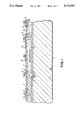
- FIG. 1 is a cross-sectional view of a portion of a high-voltage silicon-on-insulator integrated circuit including a diffused contact region in the substrate, a high voltage interconnect bus and a source-follower device.
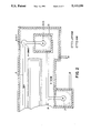
- FIG. 2 is a plan view of a portion of silicon-on-insulator circuit including a high-voltage diode, a diode operating in a source-follower mode, and a high-voltage interconnect bus
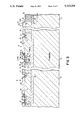
- FIG. 3 is a cross-sectional view illustrating the structure of a bridge circuit comprising two lateral-double-diffused metal-oxide-semiconductor-silicon-on insulator (LDMOS-SOI) transistors in a source-follower circuit.
- LDMOS-SOI metal-oxide-semiconductor-silicon-on insulator
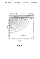
- FIG. 4 is an equipotential contour map, produced by computer simulation, of the electrostatic potential distribution in the LDMOS transistor operating in a grounded source configuration, in the bridge circuit shown in FIG. 3.
- FIG. 5 is an equipotential contour map produced by computer simulation, of the electrostatic potential distribution in the LDMOS transistor operating in a source-follower configuration, in the bridge circuit shown in FIG. 3.
- diffusion regions For a large integrated circuit, several such diffusion regions may be provided. These are placed in the parts of the chip where there are high voltage components and spaced within a few hundred micrometers away from the high voltage components. Alternatively, metal interconnections may be provided, as described below which help the lateral spreading of the depletion region, in the substrate to encompass the entire extent of the integrated circuit.
- the substrate is a silicon substrate, usually of a high resistivity p-type silicon 100 ohm-cm resistivity or greater.
- the insulating layer is a silicon oxide layer.
- the positive interfacial charge usually present at the silicon-silicon oxide interface aids in the spreading of the depletion region over large distances that sometimes exceed 1 cm.
- the diffused area is an n-type diffusion area.
- the invention is also applicable to an n-type silicon substrate provided with a p-type diffusion area.
- the semiconductor layer is preferably a substantially n-type monocrystalline silicon layer.
- the invention is particularly useful for integrated circuits adapted for high voltage applications.
- the invention has been found to be useful for circuit structures which contain devices or subcircuit regions capable of operating in a source-follower mode.
- these improved structures comprise a semiconductor substrate of a first conductivity type and an insulating layer provided on the substrate, a semiconducting layer of a second conductivity type provided on the insulating layer, a diffusion layer of a second conductivity type opposite to the first conductivity type provided in the substrate which diffusion area is laterally separated from other components of the circuit and is held at a voltage at least equal to the highest potential of source and drain portions.
- These source and drain portions are parts of isolated devices or subcircuit regions capable of operating in a source-follower mode and high voltage interconnections preferably provided by metal bus lines.
- this diffusion area is positioned so that it has no overlying non contacting circuit elements. Additionally it is preferred that the diffusion area be held at a voltage that is higher than the highest potential of any subcircuit in the device.
- FIG. 1 The basic function of the present invention is illustrated in FIG. 1. Although a high-voltage diode is shown in this illustration, the same principle can be applied to other high-voltage devices.
- a substrate 1 is made of high-resistivity p-type silicon (100 ohm-cm resistivity or greater ).
- An n-type diffusion region 2 is formed in the substrate 1, as described in detail below.
- the portion of the integrated circuit in SOI layer 3, provided between oxide layers 5 and 7 in contact with the n-type diffusion region 2, is isolated from the remainder of the integrated circuit by oxide trenches 9 to form an n-type island 11 which is biased to the most positive potential in the entire circuit (700V) through N+contact 13 and metal bus 15, while the substrate 1 is at ground potential.
- the depletion region spreads out from the n-type diffusion region 2 through the p-type substrate 1 and under the oxide layer 5 beneath other portions of the integrated circuit.
- the ability to achieve interconnects between high-voltage components in the circuit is illustrated by the regions 11 and 16 in FIG. 1.
- a p-type region 17 which is held at a ground potential (0V). Since the n-type diffusion region 2 is held at 700V, the entire n-type island 11 becomes depleted, as is the p-type substrate 1 under the island. Thus it is possible to route a metal bus 16 at high voltage (700V) from one part of the circuit to another.
- the so-called source-follower operation of a device wherein the device or a sub-section of the circuit may exist at any potential below that of the diffused n-type region is illustrated by the region 19 in FIG. 1.
- the n-type contact 21 and metal bus 22 represent the portion of this region that exists at a high (700-V) potential
- the p-type contact 23 represents the portion that can exist at either high or low potential (0-700V)
- a metal "field plate" 25 extending from region 19 over a portion of the adjacent island 3 helps the depletion region to spread through island 11 and region 19 thus preventing breakdown when region 19 is at a high potential.
- FIG. 2 shows a plan view of a portion of a circuit to illustrate how the high voltage interconnect is routed.
- a 700 V bus line 15 makes a contact (as shown in cross-section in FIG. 1) through the n+region 13 to the diffused n-type region 2 in the substrate and connects through the metal pad 22 to the n-type contact 21 in the first diode which is operated in a "source-follower" mode.
- the peripheral p-type region 23 is provided on the periphery of the source-follower diode, but is omitted on the side where the high-voltage bus 15 enters.
- the p-type region 23 is connected by another metal bus 26 to an n-type contact 27 on the second diode, which can exist at either low or high potential.
- FIG. 3 shows an embodiment of the invention having a so-called "bridge structure", wherein one component operates at a high potential and the other at either high or low potential.
- FIG. 3 there is shown part of an integrated circuit having a source-follower bridge circuit comprising two lateral-double-diffused-metal-oxide-semiconductor silicon-on-insulator (LDMOS-SOI) transistors.
- LDMOS-SOI lateral-double-diffused-metal-oxide-semiconductor silicon-on-insulator
- region 31 represents a transistor operating in source-follower mode
- region 32 represents a transistor operating in grounded-source configuration
- region 33 contains the diffusion area in the substrate which is connected to the highest voltage in the circuit (700 V in the present example).
- the fabrication sequence of the structure in FIG. 3 is as follows.
- the starting SOI layer 34 obtained by any of the standard techniques described above, such as, for example, zone-melting recrystallization or direct bonding is formed on substrate 35.
- the substrate is preferably p-type silicon of 100 ohm-cm or greater resistivity
- the thickness of the buried oxide insulator 36 is preferably 0.5-5 micrometers
- the top SOI layer 34 is preferably 0.5-10 micrometers thick n-type silicon of 10 ohm-cm or greater resistivity.
- the SOI layer 34 is implanted with phosphorus ions (through a standard 600 angstrom screen oxide) to obtain the proper resistivity required for optimum breakdown voltage, as set out in the teaching of Appels and Vaes (IEDM Proc. 1979, p. 238).
- a implantation dose of 0.5-2 ⁇ 10 12 /cm 2 at 50 KeV, followed by diffusion at 1150° C. for approximately 6 hours is employed.
- Trench isolation regions 37 are formed as follows. A 3000 angstrom silicon nitride layer (not shown) is deposited, by standard chemical vapor deposition, over a standard 600 angstrom pad oxide (not shown) on the surface of the SOI layer 34. Then a 7000 angstrom silicon dioxide layer (not shown) is deposited, by standard chemical vapor deposition, on the layer of silicon nitride. A photoresist mask layer (not shown) is used to selectively expose those regions where trenches are desired. The silicon dioxide, silicon nitride, and pad oxide layers are, respectively, removed (in the unmasked areas) by reactive ion etching.
- the full thickness of the SOI layer 34 is etched (also by reactive ion etching), employing the deposited silicon dioxide layer as a mask. This leaves 1-2 ⁇ m-wide trenches throughout the SOI layer. 1-2 ⁇ m of silicon dioxide is then deposited at a temperature of approximately 1000° C., to fill the trenches. A planarization etch of the silicon dioxide and silicon nitride layers completes this step.
- the buried diffusion region 41 is formed as follows. Layers (not shown) of silicon nitride (1400 angstroms), polysilicon (3500 angstroms), and silicon dioxide (7000 angstroms), respectively, are deposited by standard chemical vapor deposition. Areas for trenches through which the buried diffusion will be formed are defined in a photoresist mask layer (not shown). Layers of silicon dioxide, polysilicon, and silicon nitride, respectively, are removed by reactive ion etching. The photoresist layer is then stripped and the SO layer 34 and buried silicon dioxide layer 36 are removed by reactive ion etching, employing the top silicon dioxide layer g as a mask, thereby forming trenches.
- a 600 angstrom screen oxide is grown at the trench bottoms and walls. Phosphorus is then implanted in a dose of 4 ⁇ 10 15 /cm 2 at 100 KeV. This forms a separate buried N layer for each trench. A continuous buried N layer 41 will form later when the P body region 49 is diffused.
- the screen oxide at the bottom and sides of the trenches is removed, followed by the deposition of 2 ⁇ m of polysilicon, in-situ doped to a sheet resistance of 30 ⁇ /sq., to form a N+ contact 43 to the buried N layer 41.
- a planarization etch of the polysilicon and silicon nitride layers completes this step.
- the polysilicon gate 45 is formed as follows. The pad oxide used in the previous step is stripped and a 600 angstrom gate oxide 47 is grown. 5000 angstroms of polysilicon is deposited and the gate region is masked with a photoresist (not shown). The unmasked polysilicon regions are then removed by reactive ion etching. The photoresist is then removed.
- the P body region 49 is formed as follows. Boron ions are implanted (dose 4.4 ⁇ 10 13 /cm 2 and energy 80 KeV) in region 49, using a photoresist mask (not shown). The photoresist mask is such that the implantation is self-aligned to the polysilicon gate 45. After stripping the photoresist, the wafer is annealed at 1100° C. for approximately 20 hours. This drives the P body region 49 to a depth of approximately 5 ⁇ m (i.e. the SOI layer 34 thickness). The diffusion also spreads about 3.5 ⁇ m laterally, forming the channel region 51. In addition the multiple buried N layers diffuse to form a single continuous N buried layer 41.
- An N+ source 53 and drain 55 are formed as follows. Arsenic ions are implanted (dose 7.5 ⁇ 10 15 /cm 2 and energy 190 KeV) in the source 53, drain 55 regions, and atop the N buried layer 38 using a photoresist mask (not shown). After stripping the photoresist, the wafer is annealed at 950° C. for approximately 1 hour. This is done in such a way that 300 angstroms of silicon dioxide (not shown) grows on the polysilicon gate 45 to insulate it.
- the P+ region 57 is formed by implanting Boron (dose 4.0 ⁇ 10 15 /cm 2 and energy 40 KeV) in region 57, using a photoresist mask (not shown), and subsequently stripping the photoresist.
- Aluminum contact 59 to source 53, aluminum contact 61 to gate 45, aluminum contact 63 to drain 55 and aluminum contact 63 to N+ contact 43 to the buried diffusion layer 41 are formed as follows. 1.3 ⁇ m of silicon dioxide (8% phosphorus) is deposited onto the wafer. This layer is then masked with photoresist, exposing only those regions where aluminum contacts are desired. The silicon dioxide is removed by reactive ion etching, and the photoresist is then stripped. The wafer is annealed at approximately 1000° C. for 30 minutes to smooth the etched silicon dioxide layer thus allowing better aluminum coverage. After etching any residual silicon dioxide from the contact areas, a 1.2 ⁇ m layer of aluminum (1% silicon, 25 ⁇ sq.) is deposited.
- silicon dioxide 8% phosphorus
- a photoresist mask is used to selectively expose regions in which the aluminum will be removed.
- the aluminum is then reactive ion etched to form separate contacts to source, gate, drain, etc., as shown. After stripping the photoresist, the wafer is alloyed at 407° C. for 30 minutes.
- the final step involves the deposition of a 1.2 ⁇ m layer (not shown) of silicon dioxide (6% phosphorus) to protect the devices.
- Pad areas (not shown), used for making external electrical connections, are patterned with a photoresist mask and then opened by wet chemical etching.
- FIG. 4 and FIG. 5 are equi-potential contour maps formed by computer simulation of the devices constituting the bridge circuit represented in FIG. 3 in which the applied voltage to the drain of the source-follower transistor diffused area is 700 volts.
- FIG. 4 shows the map for the device operating in the common-source configuration
- FIG. 5 shows the map for the device operating in the source follower configuration.
- the calculated breakdown voltage exceeds 700 volts and the potential contours are uniformly spaced indicating the electric field to be uniform as is required for the realization of maximum possible breakdown voltage.
- the method of the invention may readily be applied to high-voltage integrated circuits containing other dielectrically isolated devices such as diodes and insulated gate bipolar transistors.
- the isolation of the devices may be readily achieved by use of the isolation trenches a shown.
- the presence of only a single buried diffusion area is sufficient to provide an improvement in the voltage breakdown characteristics of the integrated circuit.
Abstract
Description
Claims (14)
Priority Applications (5)
| Application Number | Priority Date | Filing Date | Title |
|---|---|---|---|
| US07/628,307 US5113236A (en) | 1990-12-14 | 1990-12-14 | Integrated circuit device particularly adapted for high voltage applications |
| DE69129617T DE69129617T2 (en) | 1990-12-14 | 1991-12-06 | Integrated circuit arrangement, particularly suitable for high-voltage applications |
| EP91203189A EP0490437B1 (en) | 1990-12-14 | 1991-12-06 | Integrated circuit device particularly adapted for high voltage applications |
| KR1019910022656A KR100257412B1 (en) | 1990-12-14 | 1991-12-11 | Integrated circuit device |
| JP33071191A JP3423006B2 (en) | 1990-12-14 | 1991-12-13 | Integrated circuit device |
Applications Claiming Priority (1)
| Application Number | Priority Date | Filing Date | Title |
|---|---|---|---|
| US07/628,307 US5113236A (en) | 1990-12-14 | 1990-12-14 | Integrated circuit device particularly adapted for high voltage applications |
Publications (1)
| Publication Number | Publication Date |
|---|---|
| US5113236A true US5113236A (en) | 1992-05-12 |
Family
ID=24518339
Family Applications (1)
| Application Number | Title | Priority Date | Filing Date |
|---|---|---|---|
| US07/628,307 Expired - Lifetime US5113236A (en) | 1990-12-14 | 1990-12-14 | Integrated circuit device particularly adapted for high voltage applications |
Country Status (5)
| Country | Link |
|---|---|
| US (1) | US5113236A (en) |
| EP (1) | EP0490437B1 (en) |
| JP (1) | JP3423006B2 (en) |
| KR (1) | KR100257412B1 (en) |
| DE (1) | DE69129617T2 (en) |
Cited By (32)
| Publication number | Priority date | Publication date | Assignee | Title |
|---|---|---|---|---|
| US5338965A (en) * | 1992-03-26 | 1994-08-16 | Texas Instruments Incorporated | High voltage structures with oxide isolated source and RESURF drift region in bulk silicon |
| US5373183A (en) * | 1993-04-28 | 1994-12-13 | Harris Corporation | Integrated circuit with improved reverse bias breakdown |
| US5378912A (en) * | 1993-11-10 | 1995-01-03 | Philips Electronics North America Corporation | Lateral semiconductor-on-insulator (SOI) semiconductor device having a lateral drift region |
| US5382818A (en) * | 1993-12-08 | 1995-01-17 | Philips Electronics North America Corporation | Lateral semiconductor-on-insulator (SOI) semiconductor device having a buried diode |
| US5412241A (en) * | 1991-02-01 | 1995-05-02 | Philips Electronics North America Corp. | Method for making an improved high voltage thin film transistor having a linear doping profile |
| US5548150A (en) * | 1993-03-10 | 1996-08-20 | Kabushiki Kaisha Toshiba | Field effect transistor |
| US5554872A (en) * | 1991-05-13 | 1996-09-10 | Kabushiki Kaisha Toshiba | Semiconductor device and method of increasing device breakdown voltage of semiconductor device |
| US5554546A (en) * | 1993-01-04 | 1996-09-10 | Texas Instruments Inc. | Method of fabricating a high voltage transistor |
| US5621239A (en) * | 1990-11-05 | 1997-04-15 | Fujitsu Limited | SOI device having a buried layer of reduced resistivity |
| US5648671A (en) * | 1995-12-13 | 1997-07-15 | U S Philips Corporation | Lateral thin-film SOI devices with linearly-graded field oxide and linear doping profile |
| US5723895A (en) * | 1995-12-14 | 1998-03-03 | Nec Corporation | Field effect transistor formed in semiconductor region surrounded by insulating film |
| US5767547A (en) * | 1991-02-01 | 1998-06-16 | U.S. Philips Corporation | High voltage thin film transistor having a linear doping profile |
| US5780311A (en) * | 1992-06-17 | 1998-07-14 | Harris Corporation | bonded wafer processing |
| US5841172A (en) * | 1995-07-06 | 1998-11-24 | Mitsubishi Denki Kabushiki Kaisha | SOI input protection circuit |
| US5877048A (en) * | 1998-03-23 | 1999-03-02 | Texas Instruments--Acer Incorporated | 3-D CMOS transistors with high ESD reliability |
| US6034399A (en) * | 1997-03-06 | 2000-03-07 | Lockheed Martin Corporation | Electrostatic discharge protection for silicon-on-insulator |
| US6121661A (en) * | 1996-12-11 | 2000-09-19 | International Business Machines Corporation | Silicon-on-insulator structure for electrostatic discharge protection and improved heat dissipation |
| US6130458A (en) * | 1996-03-28 | 2000-10-10 | Kabushiki Kaisha Toshiba | Power IC having SOI structure |
| US6133625A (en) * | 1998-03-13 | 2000-10-17 | Mitsubishi Denki Kabushiki Kaisha | Semiconductor device and method for manufacturing the same |
| KR20010023873A (en) * | 1997-09-10 | 2001-03-26 | 인피니언 테크놀로지스 아게 | Semiconductor component with a drift zone |
| SG85156A1 (en) * | 1999-01-28 | 2001-12-19 | Ibm | Method of integrating substrate contact on soi wafers with sti process |
| US20020177277A1 (en) * | 2001-04-11 | 2002-11-28 | Baliga Bantval Jayant | Power semiconductor devices having laterally extending base shielding regions that inhibit base reach through and methods of forming same |
| US20020185679A1 (en) * | 2000-06-23 | 2002-12-12 | Baliga Bantval Jayant | Power semiconductor devices having linear transfer characteristics and methods of forming and operating same |
| US6512269B1 (en) | 2000-09-07 | 2003-01-28 | International Business Machines Corporation | High-voltage high-speed SOI MOSFET |
| US6545316B1 (en) | 2000-06-23 | 2003-04-08 | Silicon Wireless Corporation | MOSFET devices having linear transfer characteristics when operating in velocity saturation mode and methods of forming and operating same |
| US20040099905A1 (en) * | 2001-04-11 | 2004-05-27 | Baliga Bantval Jayant | Power semiconductor devices having laterally extending base shielding regions that inhibit base reach-through and schottky rectifying flyback diodes |
| US6764889B2 (en) | 1998-10-26 | 2004-07-20 | Silicon Semiconductor Corporation | Methods of forming vertical mosfets having trench-based gate electrodes within deeper trench-based source electrodes |
| US20070096174A1 (en) * | 2005-11-01 | 2007-05-03 | Denso Corporation | Semiconductor device having PN junction diode and method for manufacturing the same |
| US7405982B1 (en) * | 1997-04-23 | 2008-07-29 | International Business Machines Corporation | Methods to improve the operation of SOI devices |
| US20100025763A1 (en) * | 2008-07-30 | 2010-02-04 | Maxpower Semiconductor Inc. | Semiconductor on Insulator Devices Containing Permanent Charge |
| US20100237416A1 (en) * | 2009-03-17 | 2010-09-23 | Alpha & Omega Semiconductor Incorporated | Bottom-drain ldmos power mosfet structure having a top drain strap |
| US20130320485A1 (en) * | 2012-05-30 | 2013-12-05 | X-Fab Semiconductor Foundries Ag | Semiconductor device |
Families Citing this family (6)
| Publication number | Priority date | Publication date | Assignee | Title |
|---|---|---|---|---|
| DE4233773C2 (en) * | 1992-10-07 | 1996-09-19 | Daimler Benz Ag | Semiconductor structure for semiconductor devices with high breakdown voltage |
| DE69417944T2 (en) * | 1993-04-30 | 1999-12-09 | Ibm | Process for producing a protective diode against electrostatic discharge in silicon-on-insulator technology |
| JP3061020B2 (en) | 1997-11-12 | 2000-07-10 | 日本電気株式会社 | Dielectric separated type semiconductor device |
| JPH11354631A (en) | 1998-06-11 | 1999-12-24 | Nec Kansai Ltd | Semiconductor device |
| JP2009060064A (en) * | 2007-09-04 | 2009-03-19 | New Japan Radio Co Ltd | Semiconductor device and manufacturing method therefor |
| JP5132481B2 (en) * | 2008-08-27 | 2013-01-30 | 株式会社日立製作所 | Semiconductor integrated circuit device |
Citations (5)
| Publication number | Priority date | Publication date | Assignee | Title |
|---|---|---|---|---|
| JPH01238066A (en) * | 1988-03-18 | 1989-09-22 | Fujitsu Ltd | High withstand voltage transistor |
| US4884116A (en) * | 1986-12-20 | 1989-11-28 | Kabushiki Kaisha Toshiba | Double diffused mosfet with potential biases |
| US4883543A (en) * | 1980-06-05 | 1989-11-28 | Texas Instruments Incroporated | Shielding for implant in manufacture of dynamic memory |
| US4893159A (en) * | 1985-09-25 | 1990-01-09 | Kabushiki Kaisha Toshiba | Protected MOS transistor circuit |
| US4962413A (en) * | 1987-08-14 | 1990-10-09 | Oki Electric Industry Co, Ltd. | Analog switch with minimized noise ascribable to gate capacitance |
Family Cites Families (1)
| Publication number | Priority date | Publication date | Assignee | Title |
|---|---|---|---|---|
| US3701198A (en) * | 1970-08-14 | 1972-10-31 | Bell Telephone Labor Inc | Monolithic integrated circuit structures and methods of making same |
-
1990
- 1990-12-14 US US07/628,307 patent/US5113236A/en not_active Expired - Lifetime
-
1991
- 1991-12-06 DE DE69129617T patent/DE69129617T2/en not_active Expired - Fee Related
- 1991-12-06 EP EP91203189A patent/EP0490437B1/en not_active Expired - Lifetime
- 1991-12-11 KR KR1019910022656A patent/KR100257412B1/en not_active IP Right Cessation
- 1991-12-13 JP JP33071191A patent/JP3423006B2/en not_active Expired - Fee Related
Patent Citations (5)
| Publication number | Priority date | Publication date | Assignee | Title |
|---|---|---|---|---|
| US4883543A (en) * | 1980-06-05 | 1989-11-28 | Texas Instruments Incroporated | Shielding for implant in manufacture of dynamic memory |
| US4893159A (en) * | 1985-09-25 | 1990-01-09 | Kabushiki Kaisha Toshiba | Protected MOS transistor circuit |
| US4884116A (en) * | 1986-12-20 | 1989-11-28 | Kabushiki Kaisha Toshiba | Double diffused mosfet with potential biases |
| US4962413A (en) * | 1987-08-14 | 1990-10-09 | Oki Electric Industry Co, Ltd. | Analog switch with minimized noise ascribable to gate capacitance |
| JPH01238066A (en) * | 1988-03-18 | 1989-09-22 | Fujitsu Ltd | High withstand voltage transistor |
Non-Patent Citations (6)
| Title |
|---|
| Nakashima et al "High-Voltage CMOS SIMOX Technology and its Application to a BSH-LSI" IEEE Transactions on Electron Devices vol ED 33 No. 1 Jan. 1986 pp. 126-132. |
| Nakashima et al High Voltage CMOS SIMOX Technology and its Application to a BSH LSI IEEE Transactions on Electron Devices vol ED 33 No. 1 Jan. 1986 pp. 126 132. * |
| Ratnam "Novel Silicon-on-Insulator Mosfet for High-Voltage Integrated Circuits" Electronics Letters vol. 25 No. 8, Apr. 13, 1989 pp. 536-537. |
| Ratnam Novel Silicon on Insulator Mosfet for High Voltage Integrated Circuits Electronics Letters vol. 25 No. 8, Apr. 13, 1989 pp. 536 537. * |
| Rumennik "Power Devices are in the Chips" IEEE Spectrum, vol. 22, Jul. 1985 pp. 27, 29, 31, and 33. |
| Rumennik Power Devices are in the Chips IEEE Spectrum, vol. 22, Jul. 1985 pp. 27, 29, 31, and 33. * |
Cited By (53)
| Publication number | Priority date | Publication date | Assignee | Title |
|---|---|---|---|---|
| US5621239A (en) * | 1990-11-05 | 1997-04-15 | Fujitsu Limited | SOI device having a buried layer of reduced resistivity |
| US5412241A (en) * | 1991-02-01 | 1995-05-02 | Philips Electronics North America Corp. | Method for making an improved high voltage thin film transistor having a linear doping profile |
| US5767547A (en) * | 1991-02-01 | 1998-06-16 | U.S. Philips Corporation | High voltage thin film transistor having a linear doping profile |
| US5554872A (en) * | 1991-05-13 | 1996-09-10 | Kabushiki Kaisha Toshiba | Semiconductor device and method of increasing device breakdown voltage of semiconductor device |
| US5338965A (en) * | 1992-03-26 | 1994-08-16 | Texas Instruments Incorporated | High voltage structures with oxide isolated source and RESURF drift region in bulk silicon |
| US5780311A (en) * | 1992-06-17 | 1998-07-14 | Harris Corporation | bonded wafer processing |
| US5801084A (en) * | 1992-06-17 | 1998-09-01 | Harris Corporation | Bonded wafer processing |
| US5554546A (en) * | 1993-01-04 | 1996-09-10 | Texas Instruments Inc. | Method of fabricating a high voltage transistor |
| US5686755A (en) * | 1993-01-04 | 1997-11-11 | Texas Instruments Incorporated | LDMOS resurf high voltage transistor |
| US5548150A (en) * | 1993-03-10 | 1996-08-20 | Kabushiki Kaisha Toshiba | Field effect transistor |
| US5373183A (en) * | 1993-04-28 | 1994-12-13 | Harris Corporation | Integrated circuit with improved reverse bias breakdown |
| US5378912A (en) * | 1993-11-10 | 1995-01-03 | Philips Electronics North America Corporation | Lateral semiconductor-on-insulator (SOI) semiconductor device having a lateral drift region |
| US5382818A (en) * | 1993-12-08 | 1995-01-17 | Philips Electronics North America Corporation | Lateral semiconductor-on-insulator (SOI) semiconductor device having a buried diode |
| US5841172A (en) * | 1995-07-06 | 1998-11-24 | Mitsubishi Denki Kabushiki Kaisha | SOI input protection circuit |
| US6046476A (en) * | 1995-07-06 | 2000-04-04 | Mitsubishi Denki Kabushiki Kaisha | SOI input protection circuit |
| US5648671A (en) * | 1995-12-13 | 1997-07-15 | U S Philips Corporation | Lateral thin-film SOI devices with linearly-graded field oxide and linear doping profile |
| US5723895A (en) * | 1995-12-14 | 1998-03-03 | Nec Corporation | Field effect transistor formed in semiconductor region surrounded by insulating film |
| US6130458A (en) * | 1996-03-28 | 2000-10-10 | Kabushiki Kaisha Toshiba | Power IC having SOI structure |
| US6121661A (en) * | 1996-12-11 | 2000-09-19 | International Business Machines Corporation | Silicon-on-insulator structure for electrostatic discharge protection and improved heat dissipation |
| US6352882B1 (en) * | 1996-12-11 | 2002-03-05 | International Business Machines Corporation | Silicon-on-insulator structure for electrostatic discharge protection and improved heat dissipation |
| US6034399A (en) * | 1997-03-06 | 2000-03-07 | Lockheed Martin Corporation | Electrostatic discharge protection for silicon-on-insulator |
| US7405982B1 (en) * | 1997-04-23 | 2008-07-29 | International Business Machines Corporation | Methods to improve the operation of SOI devices |
| KR20010023873A (en) * | 1997-09-10 | 2001-03-26 | 인피니언 테크놀로지스 아게 | Semiconductor component with a drift zone |
| US6133625A (en) * | 1998-03-13 | 2000-10-17 | Mitsubishi Denki Kabushiki Kaisha | Semiconductor device and method for manufacturing the same |
| US6248657B1 (en) | 1998-03-13 | 2001-06-19 | Mitsubishi Denki Kabushiki Kaisha | Semiconductor device and method for manufacturing the same |
| US5877048A (en) * | 1998-03-23 | 1999-03-02 | Texas Instruments--Acer Incorporated | 3-D CMOS transistors with high ESD reliability |
| US6764889B2 (en) | 1998-10-26 | 2004-07-20 | Silicon Semiconductor Corporation | Methods of forming vertical mosfets having trench-based gate electrodes within deeper trench-based source electrodes |
| SG85156A1 (en) * | 1999-01-28 | 2001-12-19 | Ibm | Method of integrating substrate contact on soi wafers with sti process |
| US6521947B1 (en) | 1999-01-28 | 2003-02-18 | International Business Machines Corporation | Method of integrating substrate contact on SOI wafers with STI process |
| US6784486B2 (en) | 2000-06-23 | 2004-08-31 | Silicon Semiconductor Corporation | Vertical power devices having retrograded-doped transition regions therein |
| US20020185679A1 (en) * | 2000-06-23 | 2002-12-12 | Baliga Bantval Jayant | Power semiconductor devices having linear transfer characteristics and methods of forming and operating same |
| US6545316B1 (en) | 2000-06-23 | 2003-04-08 | Silicon Wireless Corporation | MOSFET devices having linear transfer characteristics when operating in velocity saturation mode and methods of forming and operating same |
| US20050001268A1 (en) * | 2000-06-23 | 2005-01-06 | Baliga Bantval Jayant | Power semiconductor devices having linear transfer characteristics when regions therein are in velocity saturation modes and methods of forming and operating same |
| US6512269B1 (en) | 2000-09-07 | 2003-01-28 | International Business Machines Corporation | High-voltage high-speed SOI MOSFET |
| US20020177277A1 (en) * | 2001-04-11 | 2002-11-28 | Baliga Bantval Jayant | Power semiconductor devices having laterally extending base shielding regions that inhibit base reach through and methods of forming same |
| US20020175351A1 (en) * | 2001-04-11 | 2002-11-28 | Baliga Bantval Jayant | Power semiconductor devices having retrograded-doped transition regions that enhance breakdown voltage characteristics and methods of forming same |
| US6791143B2 (en) | 2001-04-11 | 2004-09-14 | Silicon Semiconductor Corporation | Power semiconductor devices having laterally extending base shielding regions that inhibit base reach-through |
| US6800897B2 (en) | 2001-04-11 | 2004-10-05 | Silicon Semiconductor Corporation | Integrated circuit power devices having junction barrier controlled schottky diodes therein |
| US20040232479A1 (en) * | 2001-04-11 | 2004-11-25 | Baliga Bantval Jayant | Methods of forming vertical power devices having trench-based source electrodes with sidewall source contacts |
| US20040099905A1 (en) * | 2001-04-11 | 2004-05-27 | Baliga Bantval Jayant | Power semiconductor devices having laterally extending base shielding regions that inhibit base reach-through and schottky rectifying flyback diodes |
| US20050032291A1 (en) * | 2001-04-11 | 2005-02-10 | Baliga Bantval Jayant | Methods of forming power semiconductor devices having laterally extending base shielding regions |
| US7041559B2 (en) | 2001-04-11 | 2006-05-09 | Silicon Semiconductor Corporation | Methods of forming power semiconductor devices having laterally extending base shielding regions |
| US6781194B2 (en) | 2001-04-11 | 2004-08-24 | Silicon Semiconductor Corporation | Vertical power devices having retrograded-doped transition regions and insulated trench-based electrodes therein |
| US20070096174A1 (en) * | 2005-11-01 | 2007-05-03 | Denso Corporation | Semiconductor device having PN junction diode and method for manufacturing the same |
| US20100025763A1 (en) * | 2008-07-30 | 2010-02-04 | Maxpower Semiconductor Inc. | Semiconductor on Insulator Devices Containing Permanent Charge |
| US10062788B2 (en) * | 2008-07-30 | 2018-08-28 | Maxpower Semiconductor Inc. | Semiconductor on insulator devices containing permanent charge |
| US20190123210A1 (en) * | 2008-07-30 | 2019-04-25 | Maxpower Semiconductor Inc. | Semiconductor on Insulator Devices Containing Permanent Charge |
| US20100237416A1 (en) * | 2009-03-17 | 2010-09-23 | Alpha & Omega Semiconductor Incorporated | Bottom-drain ldmos power mosfet structure having a top drain strap |
| US7829947B2 (en) | 2009-03-17 | 2010-11-09 | Alpha & Omega Semiconductor Incorporated | Bottom-drain LDMOS power MOSFET structure having a top drain strap |
| US20110014766A1 (en) * | 2009-03-17 | 2011-01-20 | Alpha And Omega Semiconductor Incorporated | Bottom-drain ldmos power mosfet structure having a top drain strap |
| US8198154B2 (en) | 2009-03-17 | 2012-06-12 | Alpha And Omega Semiconductor Incorporated | Method of forming bottom-drain LDMOS power MOSFET structure having a top drain strap |
| US20130320485A1 (en) * | 2012-05-30 | 2013-12-05 | X-Fab Semiconductor Foundries Ag | Semiconductor device |
| US10529866B2 (en) * | 2012-05-30 | 2020-01-07 | X-Fab Semiconductor Foundries Gmbh | Semiconductor device |
Also Published As
| Publication number | Publication date |
|---|---|
| EP0490437A1 (en) | 1992-06-17 |
| DE69129617T2 (en) | 1999-01-28 |
| KR920013780A (en) | 1992-07-29 |
| EP0490437B1 (en) | 1998-06-17 |
| DE69129617D1 (en) | 1998-07-23 |
| KR100257412B1 (en) | 2000-05-15 |
| JP3423006B2 (en) | 2003-07-07 |
| JPH04275450A (en) | 1992-10-01 |
Similar Documents
| Publication | Publication Date | Title |
|---|---|---|
| US5113236A (en) | Integrated circuit device particularly adapted for high voltage applications | |
| JP3746302B2 (en) | SOI type high voltage thin film transistor and method of manufacturing the same | |
| US5246870A (en) | Method for making an improved high voltage thin film transistor having a linear doping profile | |
| KR0163402B1 (en) | Merged bipolar/cmos technology using electrically active trench | |
| JP3431734B2 (en) | SOI field effect transistor and method of manufacturing the same | |
| US6204138B1 (en) | Method for fabricating a MOSFET device structure which facilitates mitigation of junction capacitance and floating body effects | |
| US5434444A (en) | High breakdown voltage semiconductor device | |
| US5340759A (en) | Method of making a vertical gate transistor with low temperature epitaxial channel | |
| US5130770A (en) | Integrated circuit in silicon on insulator technology comprising a field effect transistor | |
| EP0217288A2 (en) | Substrate structure for a composite semiconductor device | |
| US5874768A (en) | Semiconductor device having a high breakdown voltage | |
| US20020098656A1 (en) | Method of fabricating semiconductor device | |
| JP2002324905A (en) | Method of forming integrated circuit having body contact | |
| KR20030005385A (en) | Field effect transistor structure and method of manufacture | |
| US6294817B1 (en) | Source/drain-on insulator (S/DOI) field effect transistor using oxidized amorphous silicon and method of fabrication | |
| US6281593B1 (en) | SOI MOSFET body contact and method of fabrication | |
| US5481126A (en) | Semiconductor-on-insulator electronic devices having trench isolated monocrystalline active regions | |
| US5191397A (en) | SOI semiconductor device with a wiring electrode contacts a buried conductor and an impurity region | |
| US6232155B1 (en) | Methods of fabricating semiconductor-on-insulator devices including alternating thin and thick film semiconductor regions on an insulating layer | |
| JP3354127B2 (en) | High voltage element and method of manufacturing the same | |
| US5925916A (en) | Semiconductor processing method of providing electrical isolation between adjacent semiconductor diffusion regions of different field effect transistors and integrated circuitry having adjacent electrically isolated field effect transistors | |
| US4660278A (en) | Process of making IC isolation structure | |
| US6420767B1 (en) | Capacitively coupled DTMOS on SOI | |
| US6359298B1 (en) | Capacitively coupled DTMOS on SOI for multiple devices | |
| US20070099372A1 (en) | Device having active regions of different depths |
Legal Events
| Date | Code | Title | Description |
|---|---|---|---|
| AS | Assignment |
Owner name: NORTH AMERICAN PHILIPS CORPORATION, 100 EAST 42ND Free format text: ASSIGNMENT OF ASSIGNORS INTEREST.;ASSIGNORS:ARNOLD, EMIL;MERCHANT, STEVEN L.;SHACKLE, PETER W.;REEL/FRAME:005545/0446 Effective date: 19901211 |
|
| STCF | Information on status: patent grant |
Free format text: PATENTED CASE |
|
| FPAY | Fee payment |
Year of fee payment: 4 |
|
| FPAY | Fee payment |
Year of fee payment: 8 |
|
| FPAY | Fee payment |
Year of fee payment: 12 |
|
| AS | Assignment |
Owner name: PHILIPS ELECTRONICS NORTH AMERICA CORPORATION, NEW Free format text: CHANGE OF NAME;ASSIGNOR:NORTH AMERICAN PHILIPS CORPORATION;REEL/FRAME:022980/0424 Effective date: 19930525 Owner name: NXP B.V., NETHERLANDS Free format text: ASSIGNMENT OF ASSIGNORS INTEREST;ASSIGNOR:PHILIPS ELECTRONICS NORTH AMERICA CORPORATION;REEL/FRAME:022980/0441 Effective date: 20090715 Owner name: FGP CORP., NEW YORK Free format text: MERGER;ASSIGNOR:PHILIPS ELECTRONICS NORTH AMERICA CORPORATION;REEL/FRAME:022980/0428 Effective date: 19951201 Owner name: PHILIPS ELECTRONICS NORTH AMERICA CORPORATION, NEW Free format text: CHANGE OF NAME;ASSIGNOR:FGP CORP.;REEL/FRAME:022980/0433 Effective date: 19951201 |