US5126759A - Non-impact printer with token bit control of data and current regulation signals - Google Patents
Non-impact printer with token bit control of data and current regulation signals Download PDFInfo
- Publication number
- US5126759A US5126759A US07/543,930 US54393090A US5126759A US 5126759 A US5126759 A US 5126759A US 54393090 A US54393090 A US 54393090A US 5126759 A US5126759 A US 5126759A
- Authority
- US
- United States
- Prior art keywords
- current
- image data
- signals
- register
- driving
- Prior art date
- Legal status (The legal status is an assumption and is not a legal conclusion. Google has not performed a legal analysis and makes no representation as to the accuracy of the status listed.)
- Expired - Lifetime
Links
Images


Classifications
-
- B—PERFORMING OPERATIONS; TRANSPORTING
- B41—PRINTING; LINING MACHINES; TYPEWRITERS; STAMPS
- B41J—TYPEWRITERS; SELECTIVE PRINTING MECHANISMS, i.e. MECHANISMS PRINTING OTHERWISE THAN FROM A FORME; CORRECTION OF TYPOGRAPHICAL ERRORS
- B41J2/00—Typewriters or selective printing mechanisms characterised by the printing or marking process for which they are designed
- B41J2/435—Typewriters or selective printing mechanisms characterised by the printing or marking process for which they are designed characterised by selective application of radiation to a printing material or impression-transfer material
- B41J2/447—Typewriters or selective printing mechanisms characterised by the printing or marking process for which they are designed characterised by selective application of radiation to a printing material or impression-transfer material using arrays of radiation sources
- B41J2/45—Typewriters or selective printing mechanisms characterised by the printing or marking process for which they are designed characterised by selective application of radiation to a printing material or impression-transfer material using arrays of radiation sources using light-emitting diode [LED] or laser arrays
Definitions
- the present invention relates to non-impact printer apparatus for recording, and more specifically, to circuitry thereon for controlling data and other signals flowing to a printhead forming part of the printer apparatus.
- a grey level LED (light emitting diode) printhead is described.
- signals comprising plural digital data bits representing a time for recording a pixel (picture element) are simultaneously fed to the printhead over a data bus.
- a token bit is also provided simultaneously with the data to activate certain latch registers associated with a respective LED so that the data is distributed appropriately.
- the use of the token bit simplifies circuitry and connection pads on the printhead and thereby facilitates construction of the printhead.
- a non-impact printer apparatus that includes a recording head having a plurality of recording elements for recording on a recording medium; driving means for selectively driving said plurality of recording elements in accordance with respective image data signals; image data bus means for carrying image data signals related to an exposure duration; said driving means including respective data register means associated with each recording element for storing said image data signals; means connecting said data bus means to said data register means; said driving means further including current regulating means for regulating the level of electrical current to each recording element, the current regulating means including means for adjusting the level of current in response to a multibit digital signal; and wherein the multibit digital signal used for regulating current is carried on the image data bus means.
- a non-impact printer apparatus that includes a recording head having a plurality of recording elements for recording on a recording medium; driving means for selectively driving said plurality of recording elements in accordance with respective image data signals; said driving means including respective data register means associated with each recording element for storing said image data signals; data bus means for carrying image data signals; means commonly connecting said data bus means to said data register means; means for generating a token bit signal; a multistage shift register means for outputting sequentially at respective stages the token bit signal for sequentially selecting a respective data register means for accepting image data signals; said driving means further including current regulating means for regulating the level of electrical current to each recording element, the current regulating means including means for adjusting the level of current in response to a multibit digital signal; wherein the current regulating means includes first register means including a plurality of registers for storing digital signals related to a level of current control; second register means for storing and shifting a token bit signal; and means responsive to the token bit signal for latching in an appropriate register
- FIG. 1 is a perspective view illustrating the general arrangement of a prior art non-impact printer
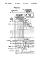
- FIG. 2 is a block diagram of a circuit for providing signals to a non-impact head made in accordance with the invention
- FIG. 3 is a block diagram of a printhead according to the invention, the printhead including a plurality of driver chips for driving the LED's formed on chip arrays;
- FIGS. 4, 4a and 4b are a block diagram of a driver chip made according to the invention.
- FIGS. 5, 5a and 5b are a circuit diagram of one circuit incorporated on the driver chip in accordance with the invention.
- FIGS. 6A, B, C and D are a schematic of a current driving circuit incorporated on the driver chip of FIG. 4.
- the apparatus for the herein disclosed invention is typified by the diagram of FIG. 1; a linear array 10 of say 3584 triggerable recording elements; e.g. LED's, is disposed to expose selectively a photosensitive image-receiver medium 12 that is movable relative to the array by suitable conventional means (not shown). Optical means for focusing the LED's onto the medium may also be provided. In this regard, gradient index optical fiber devices such as Selfoc (trademark of Nippon Sheet Glass Co., Ltd.) arrays are highly suited.
- the LED's of the array are triggered into operation by means of image processing electronics 14 that are responsive to image signal information. Depending on the duration for which any given LED is turned on, the exposure effected by such LED is more or less made.
- the latent image formed line by line by selective exposure of said LED's may be subsequently developed by conventional means to form a visible image.
- the medium 12 is an electrophotographic receptor
- the LED's may be used to form an electrostatic image on a uniformly electrostatically charged photoconductor and this image developed using opaque toner particles and perhaps transferred to a copy sheet, see U.S. Pat. Nos. 3,850,517 and 4,831,395, the contents of which are incorporated herein by this reference.
- a data source 15 such as a computer, word processor, image scanner or other source of digitized image data, provides image data signals to a data processor 16 which may comprise a raster image processor.
- the data processor under control of clock pulses from a logic and control device (LCU) 13 provides a plurality of outputs including rasterized data outputs and control signals which are fed to the print head.
- the LCU provides clock pulses via line 17 to an down/up counter 18 (FIG. 4) which, when enabled by a signal from the LCU, counts such clock pulses and provides at an output having a plurality of lines a digital signal representation of the state of the counter.
- such a counter has one line representing a least significant bit of such count and other lines representing other more significant bits.
- the output of counter 18 is provided to a first set of input terminals to a comparator 19 (see FIG. 4) associated with each recording element 30, i.e., LED in this embodiment.
- a plurality of data lines from each of a plurality of corresponding data registers 24 is provided to a second set of input terminals associated with each comparator 19.
- the comparators 19 all compare the output of the counter 18 with the value of the respective data.
- the image data signals provided to each comparator relates to a desired ON time or period of enablement for a respective LED 30 for the recording of a particular pixel.
- the LED's are alternately divided into odd and even-numbered LED's so that respective integrated circuit driver chips 40 therefor are located on opposite sides of the line of LED's.
- the discussion herein will be made as to one of these driver chips.
- the image data signals provided to each comparator 19 during the printing of a single line of dots by the row of LED's is related to the desired pixel or dot size to be exposed onto the image receiver medium by that LED for that particular line of dots. As shown in FIGS.
- six independent lines of data DI0 through DI5 provide a six bit digital image data signal that allows for grey-scale variation of the output of each LED during each cycle of operation.
- the data to each comparator may comprise six binary bits representing an amount from decimal 0 to decimal 63.
- the data lines DI0 through DI5 are shown passing through the data registers 24 in FIG. 4, it will be appreciated that this is for the convenience of this illustration and that actually such lines comprise a bus or plurality of data lines that are simultaneously available to all data registers as will be described below.
- an LED, LED 1 is to be enabled for a time period equal to 20 clock periods plus T MIN .
- T MIN represents a pre-established minimum LED on time.
- the counter 18 is enabled and commences to count exposure clock pulses from line 17 from decimal 63 to 0. Note that the clock pulses may be generated to have a variable programmable period.
- the six bit output of counter 18 is coupled to one set of inputs at terminal X of each of the comparators. This counter is now compared with the data input at another set of inputs at terminal Y of this comparator which represents in binary form decimal ten.
- a programmable read only memory device or PROM or other programmable device may store the characteristics of each LED and data for that LED can be modified to provide an input count at terminal Y that represents data modified by the exposure characteristics of the LED. For example, for an LED that is a relatively strong light emitter the PROM would modify data bits for that LED to reduce the count that otherwise would be provided at terminal Y based solely on the data.
- circuitry forming a part of the driving circuitry for distributing the image data signals to the appropriate comparator and to current driving circuits to which the present invention is particularly directed will now be described. It being understood, of course, that the invention in its broader aspects contemplates circuits that do not employ a comparator to control enablement of "ON" time.
- the driving circuitry for the LED's are provided on opposite sides of the line of LED's 20. This is a known desirable arrangement for permitting LED's to be packed closer together to provide greater image resolution capabilities for the printer.
- the circuit arrangement is an alternating one such that what may be called the even-numbered LED's have their respective driving circuitry located to one side of the line of LED's and what may be called the odd-numbered LED's have their respective driving circuitry located to the other side of the line of LED's.
- groups of, say, 64 of the odd numbered LED's will have their respective driving circuitry formed in a single integrated circuit chip and thus, for a print head having 3584 LED's on the print head, there may be 28 driving chips located on each side of the line of LED's.
- the driving chips to be identical, although locatable on either side of the line of LED's, it is desirable for design simplicity that signals traversing the length of the print head be programmably movable in either direction.
- the image data signals are output by the data processor 16 in accordance with image data signals for the odd-numbered LED's and image data signals for the even-numbered LED's. Discussion will now be made with regard to the image data signals for the even-numbered LED's, since operation and circuitry for the odd-numbered LED's is identical.
- Data lines DI0-DI5 are independent lines each carrying a signal representing a digital bit (0 or 1) so that together their respective signals define a digital six bit number from decimal 0 to decimal 63.
- This image data signal is passed along lines DI0-DI5 on the printhead which comprise an image data signal bus.
- a data register means 24 for latching data from this bus during each cycle of operation for printing a single line of dots or pixels.
- a token bit is used to enable a data register means associated with a particular LED to accept the data while other data register means associated with other LED's await their respective data.
- the pair of latches are connected in a master-slave relationship wherein in response to a token bit signal at the enable input terminal of the master latch 25, an image data signal at the data input terminal of the master latch 25 will cause the output of the master latch to either change or remain the same depending upon the image data signal.
- the six master latches 25 in the data register means of each LED are commonly connected to a line 27 to simultaneously receive the token bit signal from the token bit shift register 28.
- the token bit shift register 28 comprises a series of flip-flops 29 which have clock pulses (SHFTCLK) applied to the clock terminals thereof and the signal representing the token bit input to the data input terminal of each. Note that the same token bit signal will be provided to both the even and odd token bit shift registers for the even and odd numbered LED's.
- the output of each of these flip-flops 29 is connected to the data input terminal of the next flip-flop 29 in the series.
- Buffers 31 with enable inputs and direction controls are coupled to the token bit shift register 28 so that programmable control may be made of the direction for shifting the token bit along the token bit shift register 28. In the example where the token bit is to be shifted from left to right in FIG.
- the signal line TDIR (token direction) is made at an appropriate logic level to allow the token bit on line LTOKEN to pass from left to right.
- the token bit is passed from stage to stage (left to right in FIG. 4) of the token bit shift register 28 and accordingly outputted sequentially over respective lines 21 through OR gates 11 to lines 27 for enablement of all the master latches 25 of a respective data register 24.
- the data bits occurring on lines DI0-DI5 are accepted by the data registers 24 in turn from left to right until all the 1792 data registers on this side of the print head have acquired their respective six bits of data.
- a latch enable signal is then pulsed high on line LLATCHN to cause the respective slave latches 26 to latch the data at their respective outputs and to reset the toggle flip-flops 22.
- the respective outputs of the slave latches 26 are now communicated to the data input terminals Y of the respective comparators 19 for determining the duration of exposure for each LED in accordance with the techniques described above.
- the comparators 19 each have at an output an AND gate 19' and a D type flip-flop 19" in order to prevent the propagation of extraneous logic glitches from the comparator outputs to the toggle flip-flop inputs.
- the master latches 25 are now free to receive the image data signals for the next line of dots to be recorded.
- each driver chip 40 The respective outputs of the toggle flip-flops 22 are fed over respective lines 45 1 , 45 3 , and the following lines not shown 45 5 , --- 45 125 and 45 127 . As may be seen each of these lines is actually a double line one of which carries an enable signal to turn the respective LED on the other carries a complement of this signal.
- the lines 45 1 are input to respective control electrodes of transistors Q 426 , Q 427 . These transistors act as swithces and form a part of a current mirror driving circuit that includes a master circuit formed by transistors Q 424 , Q 425 and a series of digitally controlled transistors.
- these digitally controlled transistors may be selectively turned on to establish a signal I (CHIP BIAS) to thereby regulate a desired current level for the LED's driven by this driver chip.
- I CHIP BIAS
- FIG. 6C circuitry for driving two LED's, i.e., LED 1 and LED 3 are illustrated; it being understood that the driver chip would have appropriate circuits typified by those described below for driving say 64 of the odd-numbered LED's in an LED chip array having, for example, 128 LED's. Another driver chip on the other side of the LED chip array would be used to drive the 64 even-numbered LED's.
- the current through the master circuit establishes a potential V G1 on line 117.
- two transistors Q 428 , Q 429 Directly in series with LED 1 are two transistors Q 428 , Q 429 .
- Transistor Q 428 is biased to be always conductive while transistor Q 429 is switched on and off and thus is the transistor controlling whether or not current is driven to LED 1 .
- the gate or control electrode of transistor Q 429 is coupled to the drain-source connection of transistors Q 426 , Q 427 .
- transistor Q 427 When LED 1 is to be turned on, transistor Q 427 is made conductive and when LED 1 is to be turned off, transistor Q 426 is made conductive.
- the gate of transistor Q 426 receives a logic signal that is the inverse of that to gate Q 427 from a data driven enabling means 22 that is the circuitry of FIG. 4 which controls whether or not an LED is to be turned on and for how long.
- the LED is to be turned on for a duration determined by the grey level data signals input
- an additional current mirror that includes two slave circuits.
- One slave circuit comprises transistors Q 420 , Q 421 and Q 430 .
- the other slave circuit comprises transistors Q 422 , Q 423 and Q 431 .
- Transistors Q 430 , Q 431 are N-channel MOSFETS while the other transistors noted above are P-channel MOSFETS.
- the currents through these slave circuits establishes a voltage level V G2 on line 114, which is the potential of the drain electrode of transistor Q 427 .
- transistor Q 426 In operation with transistor Q 429 turned off, transistor Q 426 is on and impresses approximately the voltage V cc at the gate of transistor Q 429 .
- LED 1 When LED 1 is to be turned on to record a pixel (picture element), a signal is provided by the data enabling means 22 (see FIG. 4) to the gate of transistor Q 427 to turn same on, while on inverse signal turns transistor Q 426 off.
- the capacitive load or charge existing between its gate and substrate must be removed.
- transistor Q 427 turns on, the charge on the gate terminal of transistor Q 429 discharges through transistors Q 427 and Q 430 .
- This path for discharge of the gate capacitive load at transistor Q 429 thereby provides a turn-on time not affected by the number of LED's that are sought to be simultaneously energized.
- the reason for this is that each control transistor corresponding to transistor Q 429 has its own respective path for discharge of its respective capacitive load. While the illustrated embodiment shows use of the additional current mirror circuit containing transistor Q 430 for use in discharging the control electrode of the driving transistor, it will be understood that in some circuit arrangements, charging, rather than discharging, of the control electrode may be facilitated.
- the potential difference between the gate and source terminals of transistor Q 420 remains fixed as does that of transistor Q 421 thereby establishing a voltage level V G2 on line 114 which varies with V cc although the potential difference V cc -V G2 remains constant.
- the voltage level V G2 is established at the gate of transistor Q 429 via now conducting transistor Q 427 .
- the voltage level at the source terminal of transistor Q 429 is now at a fixed threshold value above that of V G2 .
- Transistor Q 429 acting as a cascode transistor and having its source terminal connected to the drain terminal of transistor Q 428 , thereby establishes the drain potential of the transistor Q 428 as varying with changes in V cc .
- the potential difference V GS1 is constant even though V cc itself varies.
- the voltage relationships between the various terminals of transistor Q 428 are not affected by variations in V cc and the current to LED 1 during a period for recording a pixel stays constant.
- transistor Q 429 conducts current to LED 1 for a time period controlled by the data bits for recording an appropriate pixel.
- the level of current for recording this pixel is controlled by the current mirror which is responsive to the current level I(CHIP BIAS).
- this current, I(CHIP BIAS) is controlled by three factors comprising a temperature compensated current source 172, a first group of eight digitally controlled NMOSFET transistors Q 25 , Q 26 . . . , Q 31 , Q 32 and a second group of eight digitally controlled NMOSFET transistors Q 5 , Q 6 . . . , Q 11 , Q 12 .
- Non-digitally controlled NMOSFET transistor Q 33 Associated with the first group is a non-digitally controlled NMOSFET transistor Q 33 .
- non-digitally controlled NMOSFET transistor Q 13 Associated with the second group is non-digitally controlled NMOSFET transistor Q 13 .
- Transistors Q 25 , . . . , Q 32 are parallel connected transistors whose respective gate width to gate length ratios are scaled so that their respective currents are scaled or weighted in powers of two.
- respective gate width to gate length ratios may be 256/5:128/5:64/5:32/5:16/5:8/5:4/5:2/5 and 321.5/5 for non-digitally controlled transistor Q 33 .
- Each digitally controlled transistor is controlled by a logic signal applied to a respective two-transistor switch circuit associated with the transistor.
- the circuit defined by NMOSFET transistors Q 250 and Q 251 cause current to flow through transistor Q 25 when a high level logic signal is applied to the gate of transistor Q 250 and a complementary low logic signal is applied to the gate of transistor Q 251 .
- the logic signals for controlling which of the current-carrying transistors are to be turned on are controlled by a register R 2 which stores an 8-bit digital word and its 8-bit complement representing a desired current control signal to turn on respective ones of the eight current conducting transistors Q 25 , . . . Q 32 .
- this group of transistors is used for "localized" control of LED current.
- the digital word stored in register R 2 is specific for this driver chip and will be determined by adjustment of driver current to the LED's driven by this driver chip until the LED's each provide a desired light output level.
- This digital word may be input to the register R2 from memory in the LCU or from a separate memory such as a ROM provided on the printhead.
- This digital word may also be changed in response to the temperature of the driver chip as will be described below. Briefly, the level of current from an extra current mirror channel (#65) on each driver chip is used as a measure of temperature.
- a voltage generated by this current is digitized and compared by the LCU with a value based on the digital words in register R1 and R2.
- the LCU "writes" a new digital word into register R2, if a change in current level is required according to an algorithm stored in memory.
- the LCU is programmed to provide or default to a particular set of digital words for placement into registers R 1 or R 2 .
- the LCU may be programmed to maintain a count of prior activations of each LED and adjust a control voltage according to a program based on the aging characteristics of the printhead.
- This digital word controls 8 current-carrying NMOSFET transistors Q 5 , . . . , Q 12 .
- Associated with this group of transistors is a continuously conducting NMOSFET transistor Q 13 .
- Exemplary gate width to length ratios for weighted digitally controlled transistors Q 5 -Q 12 are 896/5:448/5:224/5:112/5:56/5:28/5:14/5:7/5 and 4027/5 for non-digitally controlled transistor Q 13 .
- the 8-bit word and its 8-bit complement stored in register R 1 is the same as that stored in identical registers R 1 on the other driver chips. As the printhead ages, a new 8-bit digital word and its 8-bit complement is calculated by the LCU and input into the registers R 1 .
- the calculation of this 8-bit word for aging may be based on empirical determinations made using similar printheads or based upon a calibration of this printhead using an optical sensor that senses the output from each or selected LED's or by sensing patches recorded on the photoconductor.
- a third factor for adjustment to maintain LED uniformity of light output from chip-to-chip is a temperature compensated current source 172.
- This current source includes a temperature sensor and circuitry which will assist in boosting current to the LED's in response to increases in temperature.
- Various circuits for accomplishing this are well known for example, see Gray and Meyer, Analysis and Design of Analog Integrated Circuits, 2nd edition, pages 733-735 and figure 12.28, the contents of which are incorporated by this reference.
- V T thermo voltage
- the operation of the circuit of FIGS. 6A, B and C and D will now be described.
- the temperature compensated current I o is conducted to ground via NMOSFET transistor Q 33 and some, all or none of the transistors Q 32 , Q 31 , . . . and Q 25 depending upon the digital 8-bit signal and its 8-bit complement stored in register R 2 .
- the voltage level at the source terminal of Q 33 is determined.
- switching transistors are associated with each of these digitally controlled transistors.
- transistor Q 25 is controlled by switching transistors Q 250 and Q 251 in response to a signal causing Q 250 to conduct and Q 251 to turn off. The others are controlled similarly.
- This voltage level, V TC is also applied to the gate of transistor Q 13 and thereby controls the current conducted by transistor Q 13 .
- transistor Q 13 is the non-digitally controlled transistor associated with the digitally controlled transistor group Q 5 , . . . , Q 11 , Q 12 . In accordance with the digital word stored in register R 1 selected ones of these transistors are caused to conduct thereby affecting the bias current level I (CHIP BIAS) through PMOSFET transistor Q 425 .
- I bias current level
- the current through PMOSFET transistor Q 425 is equal to the current conducted by the master circuit comprised of transistor Q 424 , which current is replicated or scaled by current mirrors of PMOSFET slave transistors Q 429 , Q 429' , . . . etc., i.e., the current controlling transistors to LED 1 , LED 3 --- LED 127 , respectively, as well as the extra temperature sensing circuit using channel 65.
- Transistor Q 429 is caused to conduct when its respective logic transistors Q 426 , Q 427 are appropriately signaled by data signals indicating a pixel to be printed.
- transistor Q 427 turns on and biases the gate of transistor Q 429 to the level V G2 . Since transistors Q 424 and Q 428 have identical biasing, the current through transistor Q 429 will mirror or be scaled to that of transistor Q 424 for the time period for exposing a pixel as controlled by the duration of the logic low signal on line 45 1 (AN). As is noted in FIG. 6C, the current through Q 429 is fed to LED 1 , for the recording of a pixel. Identical current levels will be developed in the other channels directly providing current to respective other LED's. Thus, all LED's driven by this driver chip receive the same current for periods determined by their respective enablement signals and the currents thereto are appropriately adjusted to maintain constant the intensity of the LED's.
- lines SEL 1 and SEL 2 establish a two-bit selection of four possible operating modes of the token system.
- the options for these modes include a normal mode; i.e., one where the token is used for controlling image data to the appropriate registers 24 for latching image data, a load V REF mode wherein the digital current regulation word for loading register R 1 , the global bias, is established; a load R REF mode wherein the digital current regulation word for loading register R 2 , the local bias, is established.
- the fourth mode is referred to as a bias monitor mode and is used to check on the level of current sent to the LED's by sequentially operating channel 65 of each driver chip.
- the use of the token bit for image data has been described above is made when the "00" two-bit signal is established by the LCU at the inputs (SEL 2, SEL 1) of the 3:1 multiplexirs 60 and the logic set 62 which forms a part of the circuitry of FIG. 5 referred to as the "serial interface for V REF /R REF loading and bias monitoring.”
- the logic set may be in the form of interconnected logic AND gates. With a "00" signal, this serial interface is disabled. Data over lines DI0-DI5 is then appropriately latched by the master data flip-flops 25 in registers 24 as described above during shifting of the token bit over the token line LTOKEN and token registers 29. Data is then transferred in accordance with the techniques described above to control the duration of on-time for recording respective pixels.
- a global bias adjustment is called for by the LCU in response to a determination by the LCU that the criterion for the need for such adjustment is met.
- a criterion may be a count of printing activations or time.
- the LCU provides a signal "01" to lines SEL 2, SEL 1 during a non-production interval, as well as calculates, in accordance with an updating formula based on empirical data determined from aging this or similar printheads, an updated 8-bit word to be transmitted to all the driver chips.
- This updated current regulating data is transmitted serially over a single line DI5 of the image data bus (DI0-DI5) to the data input of a series of cascaded flip-flop registers 70-77, which form the register R 1 for storing signals V REF (0-7).
- the data over DI5 is shifted through these registers 70-77 in response to the token clock (TCLK) operating through and AND gate 80. Since DI5 is a line forming a part of the data bus the signal on line DI5 is available to all the driver chips and is latched simultaneously by the other driver chips. Thus, the R 1 registers of all driver chips are loaded simultaneously with the current control data signals V REF (0-7) in the above manner.
- the LCU In order to load the "localized” current regulation signals R REF (0-7) into registers R 2 , the LCU provides a "10" signal to SEL 2 and SEL 1. This enables latches to be responsive to the token clock through AND gate 82.
- the token bit carried on line LTOKEN is input via direction control gate 87 to latch register 90 and is then shifted through associated latches 91-97 in response to the token clock signal TCLK.
- the respective outputs of latches 90-97 are input to the clock inputs of registers R 2 storing the R REF (0-7) signals.
- the data on line DI5 is latched by the token bit in latches 90-97, into the respective flip-flops 98a-h that comprise registers R 2 .
- the token bit is shifted out of this driver chip and into an adjacent driver chip for latching DI5 into the R 2 register flip-flops for the current drivers in the next driver chip and so on.
- the current control data from the LCU for registers R 2 is specific or local to each driver chip even though this data is carried on a data line of an image data bus that is commonly connected to all the R 2 registers of the driver chips located on one side of the row of LED's.
- bias monitor In this mode, currenty from an extra or 65th current driver channel on each driver chip is monitored by the LCU. In this mode, monitoring is done to determine whether or not an acceptable current level is being provided by the current drivers and therefore whether or not the power to the printhead should be effectively shut down or adjusted to avoid damage or to better control output of the LED's. Additionally or alternatively, the monitoring of current serves to provide an indication of LED temperature and is useful to provide for a determination of when data should be modified to correct for loss of intensity of light output by the LED's as they heat up during use. Although the use of V RDF and R REF adjustments are used to control the level of current to the LED's driven by a particular driver chip, finer control can also be provided by control also of the pulsewidth duration of the LED's through correction of image data.
- a problem situation that is monitorable is where a cooling fan for the printhead fails and the temperature of the printhead rises during printing.
- the current level detected serves as a measure of temperature and when compared with the digital words stored in registers R 1 and R 2 indicates that a problem exists; i.e., the current level being generated is not within an expected range based on the control signals stored in registers R 1 and R 2 .
- the LCU In the bias monitor mode, the LCU provides a signal "11" to lines, SEL1 and SEL2. This causes the token clock to be clocked through AND gate 99 to enable a bias monitor register 100 which receives at its "D” input an output from a logic AND gate 101 which has as its inputs the token bit and a single bit "data" signal on data line DI5, representing whether or not the LCU is calling for monitoring of the current on this driver chip.
- line DI5 is available to all driver chips (of the odd-numbered driver chips) but it is the token bit that is shifted from driver chip to driver chip that determines which driver chip is to latch this data into its respective register.
- the outputs (regular and inverse) of the register 100 are switched and enables transistor Q T1 (FIG. 6D) which controls current through a calibrated fixed resistor R, 88, (FIG. 3) that is commonly connected to the respective transistors Q T1 , Q T3 , Q T55 of all driver chips located on one side of the row of LED's.
- the voltage level across the resistor 88 is related to the current on line 217 provided by transistor Q T1 , and this voltage level is sensed and converted by an analog to digital converter 89. A digital representation of this voltage signal is fed back to the LCU.
- the LCU determines if the current is acceptable in that chip and if power to the printhead should be shut down to the whole printhead by a suitable switch to the power supply supplying the printhead such as removing voltages V cc and V DD to the current source 172 via switch S (FIG. 6A). Note that because of the similar circuitry in channel 65 to that for the other driver channels on that chip, the current in channel 65 is similar to that of such other channels and thus is a measure of current that will flow to each LED for which the corresponding driver channel is enabled.
- the entering of the bias monitor mode is advantageously done after V REF and/or R REF changes have been made to allow the LCU to determine that a safe and/or appropriate level of current to the LED's will be provided.
- the LCU is programmed to enter this calibration mode after such changes and on any power-up operation.
- the LCU may be programmed to provide current regulation data to the printhead to lower the current level until a safe and/or otherwise appropriate level of current is detected. If a safe level is not detected, then a shutdown signal may be generated to remove power to the printhead. The LCU in this mode may count the token clock pulses and is thus able to determine which of the driver chips has the unsafe level of current.
- the voltage related signal sensed by the A/D converter is also related to the temperature of the printhead such signal may also be used by the LCU to adjust current to the LED's by changing the 8-bit (and 8-bit complements) local current regulating signals R REF stored in registers R 2 in response to an algorithm relating temperature measured and signals to be fed to a respective driver chip's registers R 2 .
- the signal relative to temperature may also be used to adjust the data signals to regulate the on-time of the LED's.
- the 65th channels on the even driver chips are also commonly connected to the input of the A/D converter 89 (FIG. 3).
- a reading of the voltage generated by a respective 65th driver channel on an even-numbered driver chip is determined by having a logic high level on the DI5 line on the even side with a corresponding low level signal on the DI5 line on the odd side since logic AND gate 101 (FIG. 5) on each driver chip passes the token bit only when the respective (odd or even) DI5 line is logic high.
- additional control circuitry may be associated with A/D converter 89 to add flexibility to the A/D converter.
- a printhead for recording has been described which provides efficient use of the electrical lines provided thereon.
- Multibit image data is effectively latched into appropriate registers in accordance with a token bit.
- Current regulation is effectively controlled using digitally addressed current regulation. Data for the image signals and current regulations are carried over the same lines, thereby reducing the need for additional lines. This reduces the number of bonding pads and connections required to be made in fabricating the printhead.
Abstract
Description
Claims (20)
Priority Applications (5)
| Application Number | Priority Date | Filing Date | Title |
|---|---|---|---|
| US07/543,930 US5126759A (en) | 1990-06-26 | 1990-06-26 | Non-impact printer with token bit control of data and current regulation signals |
| JP51210391A JP3256225B2 (en) | 1990-06-26 | 1991-06-25 | LED array printer |
| EP91912735A EP0487715B1 (en) | 1990-06-26 | 1991-06-25 | L.e.d. array printer |
| DE69122718T DE69122718T2 (en) | 1990-06-26 | 1991-06-25 | PRINTER WITH LIGHTING DIODE ARRANGEMENT |
| PCT/US1991/004488 WO1992000196A1 (en) | 1990-06-26 | 1991-06-25 | L.e.d. array printer |
Applications Claiming Priority (1)
| Application Number | Priority Date | Filing Date | Title |
|---|---|---|---|
| US07/543,930 US5126759A (en) | 1990-06-26 | 1990-06-26 | Non-impact printer with token bit control of data and current regulation signals |
Publications (1)
| Publication Number | Publication Date |
|---|---|
| US5126759A true US5126759A (en) | 1992-06-30 |
Family
ID=24170104
Family Applications (1)
| Application Number | Title | Priority Date | Filing Date |
|---|---|---|---|
| US07/543,930 Expired - Lifetime US5126759A (en) | 1990-06-26 | 1990-06-26 | Non-impact printer with token bit control of data and current regulation signals |
Country Status (1)
| Country | Link |
|---|---|
| US (1) | US5126759A (en) |
Cited By (59)
| Publication number | Priority date | Publication date | Assignee | Title |
|---|---|---|---|---|
| US5327524A (en) * | 1992-12-28 | 1994-07-05 | Eastman Kodak Company | Electrophotographic recording with multiple-bit grey level LED printhead with enhanced addressability |
| US5367383A (en) * | 1992-11-27 | 1994-11-22 | Eastman Kodak Company | Method and apparatus for maximizing data storage in a processor of image data |
| US5367362A (en) * | 1993-07-28 | 1994-11-22 | Eastman Kodak Company | Electronic reproduction apparatus and method with check for improper document feed |
| US5384646A (en) * | 1992-11-27 | 1995-01-24 | Eastman Kodak Company | Marking engine for grey level printing having a high productivity image data processing mode |
| US5393987A (en) * | 1993-05-28 | 1995-02-28 | Etec Systems, Inc. | Dose modulation and pixel deflection for raster scan lithography |
| US5396078A (en) * | 1993-09-22 | 1995-03-07 | Hewlett-Packard Company | Printer with optical data link to carriage |
| US5455681A (en) * | 1992-11-16 | 1995-10-03 | Eastman Kodak Company | Low resolution grey level printing method from high resolution binary input file |
| US5493322A (en) * | 1993-04-01 | 1996-02-20 | Eastman Kodak Company | Electrophotographic image forming apparatus with non-uniformity correction of recording elements |
| US5581295A (en) * | 1992-11-27 | 1996-12-03 | Eastman Kodak Company | Method and apparatus for resequencing image data for a printhead |
| US5585836A (en) * | 1993-12-27 | 1996-12-17 | Eastman Kodak Company | Electrophotographic image recording apparatus and method with correction for bow in placement of recording elements |
| US5668587A (en) * | 1994-03-04 | 1997-09-16 | Xerox Corporation | Automatic LED printbar uniformity and adjustment |
| US5805197A (en) * | 1995-12-28 | 1998-09-08 | Eastman Kodak Company | Driver IC with automatic token direction self-sensing circuitry |
| US5812174A (en) * | 1992-08-03 | 1998-09-22 | Canon Kabushiki Kaisha | Device for driving a laser diode and an electrophotography type image forming apparatus using the same |
| US5859657A (en) * | 1995-12-28 | 1999-01-12 | Eastman Kodak Company | Led printhead and driver chip for use therewith having boundary scan test architecture |
| US5917535A (en) * | 1994-01-14 | 1999-06-29 | Xerox Corporation | Digital LED printer with improved data flow and control |
| US5926201A (en) * | 1995-12-28 | 1999-07-20 | Eastman Kodak Company | Driver IC configurable for recording in multiple resolutions printhead including the driver IC and method of operating the printhead |
| US6061078A (en) * | 1997-12-23 | 2000-05-09 | Eastman Kodak Company | Non-impact printer apparatus and method of printing with improved control of emitter pulsewidth modulation duration |
| US6476845B2 (en) | 2000-12-13 | 2002-11-05 | Hewlett-Packard Co. | Electrophotographic printer, and method of controlling light emitting elements in an electrophotographic print head |
| US6606330B2 (en) | 2001-05-07 | 2003-08-12 | Lexmark International, Inc. | Laser drive compensation by duty cycle and power |
| US20050140773A1 (en) * | 2003-12-23 | 2005-06-30 | O'hara Shawn E. | Flexible printhead width |
| US20050200661A1 (en) * | 2003-12-23 | 2005-09-15 | O'hara Shawn E. | Dual input bi-directional printhead driver integrated circuit |
| US20070091131A1 (en) * | 2004-06-02 | 2007-04-26 | Canon Kabushiki Kaisha | Head substrate, printhead, head cartridge, printing apparatus, and method for inputting/outputting information |
| US20070127932A1 (en) * | 2005-12-01 | 2007-06-07 | Bing Qi | Method, system and apparatus for optical phase modulation based on frequency shift |
| US20070285459A1 (en) * | 2004-06-02 | 2007-12-13 | Canon Kabushiki Kaisha | Head substrate, printhead, head cartridge, and printing apparatus |
| US20080166149A1 (en) * | 2006-12-05 | 2008-07-10 | Oki Data Corporation | Drive device, LED array, LED head, and image forming apparatus provided therewith |
| US20090079364A1 (en) * | 2007-09-20 | 2009-03-26 | Oki Data Corporation | Driving device, driving circuit, LED head, and image forming apparatus |
| US20120182073A1 (en) * | 2000-10-26 | 2012-07-19 | Cypress Semiconductor Corporation | Apparatus and Method for Programmable Power Management in a Programmable Analog Circuit Block |
| US8358150B1 (en) | 2000-10-26 | 2013-01-22 | Cypress Semiconductor Corporation | Programmable microcontroller architecture(mixed analog/digital) |
| US8555032B2 (en) | 2000-10-26 | 2013-10-08 | Cypress Semiconductor Corporation | Microcontroller programmable system on a chip with programmable interconnect |
| US8912005B1 (en) * | 2010-09-24 | 2014-12-16 | Life Technologies Corporation | Method and system for delta double sampling |
| US9164070B2 (en) | 2010-06-30 | 2015-10-20 | Life Technologies Corporation | Column adc |
| US9239313B2 (en) | 2010-06-30 | 2016-01-19 | Life Technologies Corporation | Ion-sensing charge-accumulation circuits and methods |
| US9269708B2 (en) | 2006-12-14 | 2016-02-23 | Life Technologies Corporation | Methods and apparatus for measuring analytes using large scale FET arrays |
| US9270264B2 (en) | 2012-05-29 | 2016-02-23 | Life Technologies Corporation | System for reducing noise in a chemical sensor array |
| US9317138B1 (en) | 2003-06-27 | 2016-04-19 | Cypress Semiconductor Corporation | Method and apparatus for sensing movement of a human interface device |
| US9404920B2 (en) | 2006-12-14 | 2016-08-02 | Life Technologies Corporation | Methods and apparatus for detecting molecular interactions using FET arrays |
| US9618475B2 (en) | 2010-09-15 | 2017-04-11 | Life Technologies Corporation | Methods and apparatus for measuring analytes |
| US9671363B2 (en) | 2013-03-15 | 2017-06-06 | Life Technologies Corporation | Chemical sensor with consistent sensor surface areas |
| US9823217B2 (en) | 2013-03-15 | 2017-11-21 | Life Technologies Corporation | Chemical device with thin conductive element |
| US9835585B2 (en) | 2013-03-15 | 2017-12-05 | Life Technologies Corporation | Chemical sensor with protruded sensor surface |
| US9841398B2 (en) | 2013-01-08 | 2017-12-12 | Life Technologies Corporation | Methods for manufacturing well structures for low-noise chemical sensors |
| US9852919B2 (en) | 2013-01-04 | 2017-12-26 | Life Technologies Corporation | Methods and systems for point of use removal of sacrificial material |
| US9927393B2 (en) | 2009-05-29 | 2018-03-27 | Life Technologies Corporation | Methods and apparatus for measuring analytes |
| US9951382B2 (en) | 2006-12-14 | 2018-04-24 | Life Technologies Corporation | Methods and apparatus for measuring analytes using large scale FET arrays |
| US9960253B2 (en) | 2010-07-03 | 2018-05-01 | Life Technologies Corporation | Chemically sensitive sensor with lightly doped drains |
| US9964515B2 (en) | 2008-10-22 | 2018-05-08 | Life Technologies Corporation | Integrated sensor arrays for biological and chemical analysis |
| US9970984B2 (en) | 2011-12-01 | 2018-05-15 | Life Technologies Corporation | Method and apparatus for identifying defects in a chemical sensor array |
| US9995708B2 (en) | 2013-03-13 | 2018-06-12 | Life Technologies Corporation | Chemical sensor with sidewall spacer sensor surface |
| US10077472B2 (en) | 2014-12-18 | 2018-09-18 | Life Technologies Corporation | High data rate integrated circuit with power management |
| US10100357B2 (en) | 2013-05-09 | 2018-10-16 | Life Technologies Corporation | Windowed sequencing |
| US10379079B2 (en) | 2014-12-18 | 2019-08-13 | Life Technologies Corporation | Methods and apparatus for measuring analytes using large scale FET arrays |
| US10451585B2 (en) | 2009-05-29 | 2019-10-22 | Life Technologies Corporation | Methods and apparatus for measuring analytes |
| US10458942B2 (en) | 2013-06-10 | 2019-10-29 | Life Technologies Corporation | Chemical sensor array having multiple sensors per well |
| US10605767B2 (en) | 2014-12-18 | 2020-03-31 | Life Technologies Corporation | High data rate integrated circuit with transmitter configuration |
| US10718733B2 (en) | 2009-05-29 | 2020-07-21 | Life Technologies Corporation | Methods and apparatus for measuring analytes |
| US11231451B2 (en) | 2010-06-30 | 2022-01-25 | Life Technologies Corporation | Methods and apparatus for testing ISFET arrays |
| US11307166B2 (en) | 2010-07-01 | 2022-04-19 | Life Technologies Corporation | Column ADC |
| US11339430B2 (en) | 2007-07-10 | 2022-05-24 | Life Technologies Corporation | Methods and apparatus for measuring analytes using large scale FET arrays |
| CN114895612A (en) * | 2022-07-11 | 2022-08-12 | 深圳市杰美康机电有限公司 | Simulation system and simulation control method for DSP chip |
Citations (8)
| Publication number | Priority date | Publication date | Assignee | Title |
|---|---|---|---|---|
| US3850517A (en) * | 1972-09-25 | 1974-11-26 | Xerox Corp | High speed printout system |
| US4168531A (en) * | 1978-01-24 | 1979-09-18 | General Electric Company | Real-time clock having programmable time initialization and read-out |
| US4598358A (en) * | 1980-02-11 | 1986-07-01 | At&T Bell Laboratories | Pipelined digital signal processor using a common data and control bus |
| US4746941A (en) * | 1987-10-13 | 1988-05-24 | Eastman Kodak Company | Dot printer with token bit selection of data latching |
| US4750010A (en) * | 1987-01-02 | 1988-06-07 | Eastman Kodak Company | Circuit for generating center pulse width modulated waveforms and non-impact printer using same |
| US4831395A (en) * | 1987-04-01 | 1989-05-16 | Eastman Kodak Company | Printer apparatus |
| US4885597A (en) * | 1988-12-27 | 1989-12-05 | Eastman Kodak Company | Non-impact printer apparatus with improved current mirror driver and method of printing |
| US5025322A (en) * | 1989-12-18 | 1991-06-18 | Eastman Kodak Company | Method and apparatus for grey level recording using multiple addressability |
-
1990
- 1990-06-26 US US07/543,930 patent/US5126759A/en not_active Expired - Lifetime
Patent Citations (8)
| Publication number | Priority date | Publication date | Assignee | Title |
|---|---|---|---|---|
| US3850517A (en) * | 1972-09-25 | 1974-11-26 | Xerox Corp | High speed printout system |
| US4168531A (en) * | 1978-01-24 | 1979-09-18 | General Electric Company | Real-time clock having programmable time initialization and read-out |
| US4598358A (en) * | 1980-02-11 | 1986-07-01 | At&T Bell Laboratories | Pipelined digital signal processor using a common data and control bus |
| US4750010A (en) * | 1987-01-02 | 1988-06-07 | Eastman Kodak Company | Circuit for generating center pulse width modulated waveforms and non-impact printer using same |
| US4831395A (en) * | 1987-04-01 | 1989-05-16 | Eastman Kodak Company | Printer apparatus |
| US4746941A (en) * | 1987-10-13 | 1988-05-24 | Eastman Kodak Company | Dot printer with token bit selection of data latching |
| US4885597A (en) * | 1988-12-27 | 1989-12-05 | Eastman Kodak Company | Non-impact printer apparatus with improved current mirror driver and method of printing |
| US5025322A (en) * | 1989-12-18 | 1991-06-18 | Eastman Kodak Company | Method and apparatus for grey level recording using multiple addressability |
Cited By (107)
| Publication number | Priority date | Publication date | Assignee | Title |
|---|---|---|---|---|
| US5812174A (en) * | 1992-08-03 | 1998-09-22 | Canon Kabushiki Kaisha | Device for driving a laser diode and an electrophotography type image forming apparatus using the same |
| US5455681A (en) * | 1992-11-16 | 1995-10-03 | Eastman Kodak Company | Low resolution grey level printing method from high resolution binary input file |
| US5367383A (en) * | 1992-11-27 | 1994-11-22 | Eastman Kodak Company | Method and apparatus for maximizing data storage in a processor of image data |
| US5384646A (en) * | 1992-11-27 | 1995-01-24 | Eastman Kodak Company | Marking engine for grey level printing having a high productivity image data processing mode |
| US5581295A (en) * | 1992-11-27 | 1996-12-03 | Eastman Kodak Company | Method and apparatus for resequencing image data for a printhead |
| US5327524A (en) * | 1992-12-28 | 1994-07-05 | Eastman Kodak Company | Electrophotographic recording with multiple-bit grey level LED printhead with enhanced addressability |
| US5493322A (en) * | 1993-04-01 | 1996-02-20 | Eastman Kodak Company | Electrophotographic image forming apparatus with non-uniformity correction of recording elements |
| US5393987A (en) * | 1993-05-28 | 1995-02-28 | Etec Systems, Inc. | Dose modulation and pixel deflection for raster scan lithography |
| US5367362A (en) * | 1993-07-28 | 1994-11-22 | Eastman Kodak Company | Electronic reproduction apparatus and method with check for improper document feed |
| US5396078A (en) * | 1993-09-22 | 1995-03-07 | Hewlett-Packard Company | Printer with optical data link to carriage |
| US5585836A (en) * | 1993-12-27 | 1996-12-17 | Eastman Kodak Company | Electrophotographic image recording apparatus and method with correction for bow in placement of recording elements |
| US5917535A (en) * | 1994-01-14 | 1999-06-29 | Xerox Corporation | Digital LED printer with improved data flow and control |
| US5668587A (en) * | 1994-03-04 | 1997-09-16 | Xerox Corporation | Automatic LED printbar uniformity and adjustment |
| US5805197A (en) * | 1995-12-28 | 1998-09-08 | Eastman Kodak Company | Driver IC with automatic token direction self-sensing circuitry |
| US5859657A (en) * | 1995-12-28 | 1999-01-12 | Eastman Kodak Company | Led printhead and driver chip for use therewith having boundary scan test architecture |
| US5926201A (en) * | 1995-12-28 | 1999-07-20 | Eastman Kodak Company | Driver IC configurable for recording in multiple resolutions printhead including the driver IC and method of operating the printhead |
| US6061078A (en) * | 1997-12-23 | 2000-05-09 | Eastman Kodak Company | Non-impact printer apparatus and method of printing with improved control of emitter pulsewidth modulation duration |
| US9843327B1 (en) | 2000-10-26 | 2017-12-12 | Cypress Semiconductor Corporation | PSOC architecture |
| US9766650B2 (en) | 2000-10-26 | 2017-09-19 | Cypress Semiconductor Corporation | Microcontroller programmable system on a chip with programmable interconnect |
| US10261932B2 (en) | 2000-10-26 | 2019-04-16 | Cypress Semiconductor Corporation | Microcontroller programmable system on a chip |
| US10020810B2 (en) | 2000-10-26 | 2018-07-10 | Cypress Semiconductor Corporation | PSoC architecture |
| US10248604B2 (en) | 2000-10-26 | 2019-04-02 | Cypress Semiconductor Corporation | Microcontroller programmable system on a chip |
| US8736303B2 (en) | 2000-10-26 | 2014-05-27 | Cypress Semiconductor Corporation | PSOC architecture |
| US8555032B2 (en) | 2000-10-26 | 2013-10-08 | Cypress Semiconductor Corporation | Microcontroller programmable system on a chip with programmable interconnect |
| US8358150B1 (en) | 2000-10-26 | 2013-01-22 | Cypress Semiconductor Corporation | Programmable microcontroller architecture(mixed analog/digital) |
| US20120182073A1 (en) * | 2000-10-26 | 2012-07-19 | Cypress Semiconductor Corporation | Apparatus and Method for Programmable Power Management in a Programmable Analog Circuit Block |
| US10725954B2 (en) | 2000-10-26 | 2020-07-28 | Monterey Research, Llc | Microcontroller programmable system on a chip |
| US6476845B2 (en) | 2000-12-13 | 2002-11-05 | Hewlett-Packard Co. | Electrophotographic printer, and method of controlling light emitting elements in an electrophotographic print head |
| US6606330B2 (en) | 2001-05-07 | 2003-08-12 | Lexmark International, Inc. | Laser drive compensation by duty cycle and power |
| US9317138B1 (en) | 2003-06-27 | 2016-04-19 | Cypress Semiconductor Corporation | Method and apparatus for sensing movement of a human interface device |
| US20050200661A1 (en) * | 2003-12-23 | 2005-09-15 | O'hara Shawn E. | Dual input bi-directional printhead driver integrated circuit |
| US7246887B2 (en) | 2003-12-23 | 2007-07-24 | Eastman Kodak Company | Dual input bi-directional printhead driver integrated circuit |
| US7236183B2 (en) | 2003-12-23 | 2007-06-26 | Eastman Kodak Company | Printhead with variable exposure width |
| US20050140773A1 (en) * | 2003-12-23 | 2005-06-30 | O'hara Shawn E. | Flexible printhead width |
| US7581821B2 (en) | 2004-06-02 | 2009-09-01 | Canon Kabushiki Kaisha | Head substrate, printhead, head cartridge, and printing apparatus |
| US7364284B2 (en) | 2004-06-02 | 2008-04-29 | Canon Kabushiki Kaisha | Head substrate, printhead, head cartridge, and printing apparatus |
| US7309120B2 (en) | 2004-06-02 | 2007-12-18 | Canon Kabushiki Kaisha | Head substrate, printhead, head cartridge, printing apparatus, and method for inputting/outputting information |
| US20070285459A1 (en) * | 2004-06-02 | 2007-12-13 | Canon Kabushiki Kaisha | Head substrate, printhead, head cartridge, and printing apparatus |
| US20070091131A1 (en) * | 2004-06-02 | 2007-04-26 | Canon Kabushiki Kaisha | Head substrate, printhead, head cartridge, printing apparatus, and method for inputting/outputting information |
| US20070127932A1 (en) * | 2005-12-01 | 2007-06-07 | Bing Qi | Method, system and apparatus for optical phase modulation based on frequency shift |
| US8149259B2 (en) * | 2006-12-05 | 2012-04-03 | Oki Data Corporation | Drive device, LED array, LED head, and image forming apparatus provided therewith |
| US20080166149A1 (en) * | 2006-12-05 | 2008-07-10 | Oki Data Corporation | Drive device, LED array, LED head, and image forming apparatus provided therewith |
| US8723903B2 (en) | 2006-12-05 | 2014-05-13 | Oki Data Corporation | Drive device, LED array, LED head, and image forming apparatus provided therewith |
| US9989489B2 (en) | 2006-12-14 | 2018-06-05 | Life Technnologies Corporation | Methods for calibrating an array of chemically-sensitive sensors |
| US10203300B2 (en) | 2006-12-14 | 2019-02-12 | Life Technologies Corporation | Methods and apparatus for measuring analytes using large scale FET arrays |
| US9269708B2 (en) | 2006-12-14 | 2016-02-23 | Life Technologies Corporation | Methods and apparatus for measuring analytes using large scale FET arrays |
| US9404920B2 (en) | 2006-12-14 | 2016-08-02 | Life Technologies Corporation | Methods and apparatus for detecting molecular interactions using FET arrays |
| US10415079B2 (en) | 2006-12-14 | 2019-09-17 | Life Technologies Corporation | Methods and apparatus for detecting molecular interactions using FET arrays |
| US10816506B2 (en) | 2006-12-14 | 2020-10-27 | Life Technologies Corporation | Method for measuring analytes using large scale chemfet arrays |
| US10502708B2 (en) | 2006-12-14 | 2019-12-10 | Life Technologies Corporation | Chemically-sensitive sensor array calibration circuitry |
| US11732297B2 (en) * | 2006-12-14 | 2023-08-22 | Life Technologies Corporation | Methods and apparatus for measuring analytes using large scale FET arrays |
| US20220340965A1 (en) * | 2006-12-14 | 2022-10-27 | Life Technologies Corporation | Methods and Apparatus for Measuring Analytes Using Large Scale FET Arrays |
| US9951382B2 (en) | 2006-12-14 | 2018-04-24 | Life Technologies Corporation | Methods and apparatus for measuring analytes using large scale FET arrays |
| US11435314B2 (en) | 2006-12-14 | 2022-09-06 | Life Technologies Corporation | Chemically-sensitive sensor array device |
| US10633699B2 (en) | 2006-12-14 | 2020-04-28 | Life Technologies Corporation | Methods and apparatus for measuring analytes using large scale FET arrays |
| US11339430B2 (en) | 2007-07-10 | 2022-05-24 | Life Technologies Corporation | Methods and apparatus for measuring analytes using large scale FET arrays |
| US20090079364A1 (en) * | 2007-09-20 | 2009-03-26 | Oki Data Corporation | Driving device, driving circuit, LED head, and image forming apparatus |
| US8184139B2 (en) * | 2007-09-20 | 2012-05-22 | Oki Data Corporation | Redundance control of temperature compensation for a LED printhead |
| US11137369B2 (en) | 2008-10-22 | 2021-10-05 | Life Technologies Corporation | Integrated sensor arrays for biological and chemical analysis |
| US9964515B2 (en) | 2008-10-22 | 2018-05-08 | Life Technologies Corporation | Integrated sensor arrays for biological and chemical analysis |
| US11692964B2 (en) | 2009-05-29 | 2023-07-04 | Life Technologies Corporation | Methods and apparatus for measuring analytes |
| US11768171B2 (en) | 2009-05-29 | 2023-09-26 | Life Technologies Corporation | Methods and apparatus for measuring analytes |
| US10718733B2 (en) | 2009-05-29 | 2020-07-21 | Life Technologies Corporation | Methods and apparatus for measuring analytes |
| US10451585B2 (en) | 2009-05-29 | 2019-10-22 | Life Technologies Corporation | Methods and apparatus for measuring analytes |
| US10809226B2 (en) | 2009-05-29 | 2020-10-20 | Life Technologies Corporation | Methods and apparatus for measuring analytes |
| US9927393B2 (en) | 2009-05-29 | 2018-03-27 | Life Technologies Corporation | Methods and apparatus for measuring analytes |
| US10641729B2 (en) | 2010-06-30 | 2020-05-05 | Life Technologies Corporation | Column ADC |
| US9164070B2 (en) | 2010-06-30 | 2015-10-20 | Life Technologies Corporation | Column adc |
| US10481123B2 (en) | 2010-06-30 | 2019-11-19 | Life Technologies Corporation | Ion-sensing charge-accumulation circuits and methods |
| US9239313B2 (en) | 2010-06-30 | 2016-01-19 | Life Technologies Corporation | Ion-sensing charge-accumulation circuits and methods |
| US11231451B2 (en) | 2010-06-30 | 2022-01-25 | Life Technologies Corporation | Methods and apparatus for testing ISFET arrays |
| US11307166B2 (en) | 2010-07-01 | 2022-04-19 | Life Technologies Corporation | Column ADC |
| US9960253B2 (en) | 2010-07-03 | 2018-05-01 | Life Technologies Corporation | Chemically sensitive sensor with lightly doped drains |
| US9958414B2 (en) | 2010-09-15 | 2018-05-01 | Life Technologies Corporation | Apparatus for measuring analytes including chemical sensor array |
| US9618475B2 (en) | 2010-09-15 | 2017-04-11 | Life Technologies Corporation | Methods and apparatus for measuring analytes |
| US20140368250A1 (en) * | 2010-09-24 | 2014-12-18 | Life Technologies Corporation | Method and system for delta double sampling |
| US8912005B1 (en) * | 2010-09-24 | 2014-12-16 | Life Technologies Corporation | Method and system for delta double sampling |
| US9110015B2 (en) | 2010-09-24 | 2015-08-18 | Life Technologies Corporation | Method and system for delta double sampling |
| US10365321B2 (en) | 2011-12-01 | 2019-07-30 | Life Technologies Corporation | Method and apparatus for identifying defects in a chemical sensor array |
| US10598723B2 (en) | 2011-12-01 | 2020-03-24 | Life Technologies Corporation | Method and apparatus for identifying defects in a chemical sensor array |
| US9970984B2 (en) | 2011-12-01 | 2018-05-15 | Life Technologies Corporation | Method and apparatus for identifying defects in a chemical sensor array |
| US10404249B2 (en) | 2012-05-29 | 2019-09-03 | Life Technologies Corporation | System for reducing noise in a chemical sensor array |
| US9270264B2 (en) | 2012-05-29 | 2016-02-23 | Life Technologies Corporation | System for reducing noise in a chemical sensor array |
| US9985624B2 (en) | 2012-05-29 | 2018-05-29 | Life Technologies Corporation | System for reducing noise in a chemical sensor array |
| US9852919B2 (en) | 2013-01-04 | 2017-12-26 | Life Technologies Corporation | Methods and systems for point of use removal of sacrificial material |
| US9841398B2 (en) | 2013-01-08 | 2017-12-12 | Life Technologies Corporation | Methods for manufacturing well structures for low-noise chemical sensors |
| US10436742B2 (en) | 2013-01-08 | 2019-10-08 | Life Technologies Corporation | Methods for manufacturing well structures for low-noise chemical sensors |
| US9995708B2 (en) | 2013-03-13 | 2018-06-12 | Life Technologies Corporation | Chemical sensor with sidewall spacer sensor surface |
| US9671363B2 (en) | 2013-03-15 | 2017-06-06 | Life Technologies Corporation | Chemical sensor with consistent sensor surface areas |
| US9823217B2 (en) | 2013-03-15 | 2017-11-21 | Life Technologies Corporation | Chemical device with thin conductive element |
| US10481124B2 (en) | 2013-03-15 | 2019-11-19 | Life Technologies Corporation | Chemical device with thin conductive element |
| US9835585B2 (en) | 2013-03-15 | 2017-12-05 | Life Technologies Corporation | Chemical sensor with protruded sensor surface |
| US10422767B2 (en) | 2013-03-15 | 2019-09-24 | Life Technologies Corporation | Chemical sensor with consistent sensor surface areas |
| US10100357B2 (en) | 2013-05-09 | 2018-10-16 | Life Technologies Corporation | Windowed sequencing |
| US10655175B2 (en) | 2013-05-09 | 2020-05-19 | Life Technologies Corporation | Windowed sequencing |
| US11028438B2 (en) | 2013-05-09 | 2021-06-08 | Life Technologies Corporation | Windowed sequencing |
| US10816504B2 (en) | 2013-06-10 | 2020-10-27 | Life Technologies Corporation | Chemical sensor array having multiple sensors per well |
| US11499938B2 (en) | 2013-06-10 | 2022-11-15 | Life Technologies Corporation | Chemical sensor array having multiple sensors per well |
| US10458942B2 (en) | 2013-06-10 | 2019-10-29 | Life Technologies Corporation | Chemical sensor array having multiple sensors per well |
| US11774401B2 (en) | 2013-06-10 | 2023-10-03 | Life Technologies Corporation | Chemical sensor array having multiple sensors per well |
| US10077472B2 (en) | 2014-12-18 | 2018-09-18 | Life Technologies Corporation | High data rate integrated circuit with power management |
| US10379079B2 (en) | 2014-12-18 | 2019-08-13 | Life Technologies Corporation | Methods and apparatus for measuring analytes using large scale FET arrays |
| US11536688B2 (en) | 2014-12-18 | 2022-12-27 | Life Technologies Corporation | High data rate integrated circuit with transmitter configuration |
| US10767224B2 (en) | 2014-12-18 | 2020-09-08 | Life Technologies Corporation | High data rate integrated circuit with power management |
| US10605767B2 (en) | 2014-12-18 | 2020-03-31 | Life Technologies Corporation | High data rate integrated circuit with transmitter configuration |
| CN114895612A (en) * | 2022-07-11 | 2022-08-12 | 深圳市杰美康机电有限公司 | Simulation system and simulation control method for DSP chip |
| CN114895612B (en) * | 2022-07-11 | 2022-09-27 | 深圳市杰美康机电有限公司 | Simulation system for DSP chip |
Similar Documents
| Publication | Publication Date | Title |
|---|---|---|
| US5126759A (en) | Non-impact printer with token bit control of data and current regulation signals | |
| US5253934A (en) | L.E.D. array printer with extra driver channel | |
| EP0936509B1 (en) | Driving circuit and led head with constant turn-on time | |
| US5389953A (en) | Non-impact printer module with improved burn-in testing capability and method using same | |
| US5990920A (en) | Driving apparatus with circuits for efficiently transferring and storing compensation data | |
| JPH03503033A (en) | Non-impact printer device and printing method with improved current mirror driver | |
| US6388695B1 (en) | Driving circuit with switching element on static current path, and printer using same | |
| EP0419255A2 (en) | Method and apparatus for controlling apparent uniformity of led printheads | |
| EP0487715B1 (en) | L.e.d. array printer | |
| WO1992000196A9 (en) | L.e.d. array printer | |
| US6683638B2 (en) | Print head and image forming apparatus using multiplexed compensation data | |
| US5264868A (en) | Non-impact printer apparatus with improved current mirror driver | |
| JP2009066921A (en) | Driving circuit, led head, and image forming device | |
| JP5008312B2 (en) | Driving device, LED head, and image forming apparatus | |
| EP0487720B1 (en) | Non-impact printer for recording in color | |
| US5166702A (en) | LED printhead with improved current mirror driver and driver chip therefor | |
| US6535235B1 (en) | Drive circuit and LED head incorporating the drive circuit | |
| US6717604B2 (en) | Array driving circuit with control voltage adjusted at both ends, and array head using same | |
| US6710794B1 (en) | Light print head | |
| JPH08169139A (en) | Led head driving circuit | |
| US5034757A (en) | LED printing array current control | |
| US20110001520A1 (en) | Driver circuit and image forming apparatus | |
| EP0308492B1 (en) | Printer apparatus | |
| JP3142450B2 (en) | Drive circuit | |
| JP2001253108A (en) | Led array printer |
Legal Events
| Date | Code | Title | Description |
|---|---|---|---|
| AS | Assignment |
Owner name: EASTMAN KODAK COMPANY, NEW YORK Free format text: ASSIGNMENT OF ASSIGNORS INTEREST.;ASSIGNORS:SMALL, JEFFREY A.;HADLEY, MARY A.;POTUCEK, MARTIN;AND OTHERS;REEL/FRAME:005459/0371;SIGNING DATES FROM 19900719 TO 19900723 |
|
| STCF | Information on status: patent grant |
Free format text: PATENTED CASE |
|
| FEPP | Fee payment procedure |
Free format text: PAYOR NUMBER ASSIGNED (ORIGINAL EVENT CODE: ASPN); ENTITY STATUS OF PATENT OWNER: LARGE ENTITY |
|
| FPAY | Fee payment |
Year of fee payment: 4 |
|
| FEPP | Fee payment procedure |
Free format text: PAYER NUMBER DE-ASSIGNED (ORIGINAL EVENT CODE: RMPN); ENTITY STATUS OF PATENT OWNER: LARGE ENTITY Free format text: PAYOR NUMBER ASSIGNED (ORIGINAL EVENT CODE: ASPN); ENTITY STATUS OF PATENT OWNER: LARGE ENTITY |
|
| FEPP | Fee payment procedure |
Free format text: PAYOR NUMBER ASSIGNED (ORIGINAL EVENT CODE: ASPN); ENTITY STATUS OF PATENT OWNER: LARGE ENTITY Free format text: PAYER NUMBER DE-ASSIGNED (ORIGINAL EVENT CODE: RMPN); ENTITY STATUS OF PATENT OWNER: LARGE ENTITY |
|
| FPAY | Fee payment |
Year of fee payment: 8 |
|
| AS | Assignment |
Owner name: NEXPRESS SOLUTIONS LLC, NEW YORK Free format text: ASSIGNMENT OF ASSIGNORS INTEREST;ASSIGNOR:EASTMAN KODAK COMPANY;REEL/FRAME:012036/0959 Effective date: 20000717 |
|
| FPAY | Fee payment |
Year of fee payment: 12 |
|
| AS | Assignment |
Owner name: EASTMAN KODAK COMPANY, NEW YORK Free format text: ASSIGNMENT OF ASSIGNORS INTEREST;ASSIGNOR:NEXPRESS SOLUTIONS, INC. (FORMERLY NEXPRESS SOLUTIONS LLC);REEL/FRAME:015928/0176 Effective date: 20040909 |
|
| FEPP | Fee payment procedure |
Free format text: PAYOR NUMBER ASSIGNED (ORIGINAL EVENT CODE: ASPN); ENTITY STATUS OF PATENT OWNER: LARGE ENTITY Free format text: PAYER NUMBER DE-ASSIGNED (ORIGINAL EVENT CODE: RMPN); ENTITY STATUS OF PATENT OWNER: LARGE ENTITY |