US5134686A - Compact vector-matrix multiplier system employing electron trapping materials - Google Patents
Compact vector-matrix multiplier system employing electron trapping materials Download PDFInfo
- Publication number
- US5134686A US5134686A US07/721,345 US72134591A US5134686A US 5134686 A US5134686 A US 5134686A US 72134591 A US72134591 A US 72134591A US 5134686 A US5134686 A US 5134686A
- Authority
- US
- United States
- Prior art keywords
- electron trapping
- trapping material
- matrix
- vector
- visible light
- Prior art date
- Legal status (The legal status is an assumption and is not a legal conclusion. Google has not performed a legal analysis and makes no representation as to the accuracy of the status listed.)
- Expired - Lifetime
Links
Images


Classifications
-
- G—PHYSICS
- G02—OPTICS
- G02F—OPTICAL DEVICES OR ARRANGEMENTS FOR THE CONTROL OF LIGHT BY MODIFICATION OF THE OPTICAL PROPERTIES OF THE MEDIA OF THE ELEMENTS INVOLVED THEREIN; NON-LINEAR OPTICS; FREQUENCY-CHANGING OF LIGHT; OPTICAL LOGIC ELEMENTS; OPTICAL ANALOGUE/DIGITAL CONVERTERS
- G02F2/00—Demodulating light; Transferring the modulation of modulated light; Frequency-changing of light
- G02F2/02—Frequency-changing of light, e.g. by quantum counters
-
- G—PHYSICS
- G11—INFORMATION STORAGE
- G11C—STATIC STORES
- G11C13/00—Digital stores characterised by the use of storage elements not covered by groups G11C11/00, G11C23/00, or G11C25/00
- G11C13/04—Digital stores characterised by the use of storage elements not covered by groups G11C11/00, G11C23/00, or G11C25/00 using optical elements ; using other beam accessed elements, e.g. electron or ion beam
Definitions
- the present invention relates to optical signal processing using electron trapping materials and, more specifically, to the use of electron trapping materials in a compact optical vector-matrix multiplier system.
- a neural network model is basically represented by a matrix-vector multiplication.
- J. J. Hopfield "Neural Networks and Physical Systems with Emergent Collective Computational Abilities", Proc. Natl. Acad. Sci. USA, 79, 2554-2558 (1982).
- Vector-matrix multiplication can be performed optically by converting the vector into matrix form, forming an image of that matrix, and optically multiplying that image with the image of a vector.
- the conversion of a vector into a matrix is accomplished by the following interconnection matri T ij : ##EQU1## where V i and V j are the ith and jth elements of the vector, and where i and j represent the row and column of the matrix elements.
- Electron trapping materials are useful in performing optical multiplications.
- multiplication can be performed by writing one image, say A, onto an electron trapping material using visible light, and then reading with IR light in a pattern representing the second image B
- the output luminescent at each pixel position is proportional to the analog product of the read intensity at that pixel and the stored value at that pixel
- a primary object of the present invention is therefore to provide a compact and versatile vector-matrix multiplier employing electron trapping materials.
- Another object of the invention is to provide a rugged vector-matrix multiplier that does not use lenses in the focusing of light within the system and thus does not have the size and sensitivity drawbacks heretofore found in other similar multiplier systems.
- a further object of the present invention is to provide an associative memory using a compact vector-matrix multiplier structure.
- a still further object of the invention is to provide a compact vector-matrix multiplier/associative memory which can be built as a chip for use in an optical computer
- a method of optically multiplying a vector and a matrix by first passing visible light through a liquid crystal device to form a visible light image of a matrix and exposing an electron trapping material to the visible light image, whereby electrons in the electron trapping material at locations corresponding to the visible light image are raised to a higher energy level where they are trapped, resulting in the storage of the matrix in the electron trapping material in the form of a density pattern of trapped electrons in the higher energy level
- infrared light is passed through the liquid crystal device to form a two dimensional infrared image of a vector, and the electron trapping material is exposed to the infrared image of the vector, the infrared light releasing the trapped electrons from the higher energy level at locations corresponding to the infrared image, resulting in an emission of visible light from the electron trapping material at those locations.
- the emission of visible light from the electron trapping material is directed to a visible light detector to obtain an electrical output representing the product of said vector and said matrix
- the matrix stored by the electron trapping material is preferably formed of binary elements of 0, +1 and -1, and a bias is initially applied to the electron trapping material by exposing said electron trapping material to a uniform application of blue light. Thereafter, the matrix elements of +1 are written with blue light into the electron trapping material and the matrix elements of -1 are written with infrared light into the electron trapping material
- the electron trapping material is capable of storing multiple matrices and can be used as an associative memory by feeding back the output from the detector and reapplying it an input vector.
- the electron trapping material is initially flooded with visible light to uniformly charge said material by raising electrons in said material to a higher energy level, where they are trapped Then the electron trapping material is subjected to infrared light at selected locations such that electrons at the selected locations are released from their traps and fall back down to a lower energy level, while the remaining locations of said material not exposed to said infrared light remain charged with trapped electrons in a pattern corresponding to a matrix to be stored Next, the electron trapping material is subjected to a two-dimensional image of a vector in the form of infrared light, the infrared light releasing trapped electrons from the higher energy level, resulting in an emission of a pattern of visible light from the electron trapping material Finally, the emission of visible light from the electron trapping material is directed to a visible light detector to obtain an electrical output representing the product of the vector and the matrix.
- the first method is implemented by a vector-matrix multiplier system that includes (1) a visible light and near infrared light source; (2) a liquid crystal television which operates either under control of a computer or in conjunction with visible and infrared polarizers and visible and infrared analyzers to provide appropriate masking of the light from the light source for creating images of the vectors and matrices to be multiplied; (3) a 2-dimensional screen of electron trapping material; (4) an array of linear detectors and thresholders; and (5) for use of the system as an associative memory, a feedback system that recirculates the output as a input for iterative vector-matrix multiplication.
- the second method is preferably implemented by a system that includes an a visible light source and an infrared diode array in place of elements (1) and (2) above.
- the entire system is preferably formed into a multilayer optoelectronic chip.
- FIG. 1 shows the excitation, activation and emission spectra of a typical electron trapping material utilized in the present invention.
- FIG. 2 shows the principles of operation of the electron trapping material used in the present invention.
- FIG. 3 shows the basic structure of the electron trapping screen.
- FIG. 4 illustrates an optical setup for the vector-matrix multiplier system employing an electron trapping screen in accordance with the present invention.
- FIG. 5 shows the operation of the liquid crystal TV in performing XOR and XNOR functions
- FIG. 6 shows how the XOR are XNOR functions properly implement the Hopfield interconnection matrix.
- FIG. 7 shows the configuration of the polarizer and analyzer to obtain the required zero diagonal matrix.
- FIGS. 8 and 9 show the 2D flat illuminator used in the invention.
- FIG. 10 shows the layering of the components of the invention to form a multilayer optoelectric chip.
- Electron trapping materials characteristically can emit different output photons which correlate spatially in intensity with input photons.
- the preferred electron trapping material of the present invention is formed of an alkaline earth metal sulfide base doped with rare earth impurities.
- a number of different electron trapping materials have been developed by the assignee of the present application. material formed of a strontium sulfide base doped with samarium and europium (SrS:Sm,Eu). This material outputs orange light centered at 620 nm.
- SrS:Sm,Eu europium
- 4,842,960 discloses a material formed of a mixed strontium sulfide/calcium sulfide base doped with samarium and europium/cerium (SrS/CaS:Sm,Eu/Ce) This material also emits orange light, but has a very high efficiency and a brighter output than the material without calcium sulfide As shown in FIG. 1, the activation wavelength of this preferred SrS/CaS:Sm,Eu/Ce material is about 450 nm, its emission wavelength is orange (about 630 nm) and it stimulation wavelength is near-infrared.
- U.S Pat. No. 4,879,186 discloses a material formed of a calcium sulfide base doped with samarium and europium (CaS Sm,Eu), which outputs red light centered at 650 nm.
- Each of the above electron trapping materials have electron traps with depths of about 1.0 to 1.2 electron volts. Further details of the materials and the processes for making the materials are set forth in the disclosure of each of the above-referred U.S. patents, which are herein incorporated by reference.
- the electron trapping materials can be used to store optical information in the form of trapped electrons. This has been described by J. Lindmayer, P. Goldsmith, and C. Wrigley, in "Electronic Optical-Storage Technology Approaches Development phase", Laser Focus World, p. 119, Nov. 1989.
- electron trapping materials are capable of performing multiplication, addition, and subtraction within a dynamic range over four orders of magnitude
- the orange/red emission intensity is proportional to the product of the blue write-in intensity and the IR readout intensity.
- the addition and subtraction are performed by increasing and decreasing the number of trapped electrons. These operations are physically carried out by exposing the electron trapping material to blue and IR light, respectively.
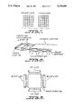
- screen 10 consists of a substrate 20 coated with an electron trapping material 30.
- the substrate 20 may be any transparent material such as glass, quartz or sapphire.
- the material 30 establishes a planar surface 16.
- An optical transparent coating 18 may encapsulate the material 30 and substrate 20.
- Material 30 is preferably deposited upon substrate 20 using thin film techniques, preferably by physical or chemical vapor deposition. Details concerning the preferred thin film deposition process are set forth in the present assignee's U.S. Pat. Nos. 4,830,875 and 4,915,982, which are herein incorporated by reference.
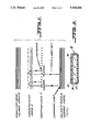
- the vector-matrix multiplier system of the present invention consists of the hardware outside of the broken lines designated by reference numeral 40
- the hardware within the broken lines is used for feedback if the system is to be used as an associative memory, described later
- Vector-matrix system 40 consists of an electron trapping screen 10 and a light illuminator 42 on opposite sides of a liquid crystal TV 44.
- LCTV 44 has separately controllable vertical electrodes 45 and horizontal electrodes 46.
- a blue light polarizer 48 and an IR polarizer 50 are disposed between illuminator 42 and LCTV 44.
- An IR analyzer 52 and blue analyzer 54 are disposed between LCTV 44 and electron trapping screen 10.
- electron trapping layer 10 is charged with visible light, and outputs visible light when stimulated by IR light.
- the visible light output from electron trapping layer 10 is detected by detector array 56, and the electrical signals from detector array 56 are differentiated by an array of thresholders 58.
- the outputs from thresholder array 58 is gated through output control 60 to parallel output 62, (or alternatively fed back to control LCTV 44 if the device is utilized as an associative memory, as described later).
- Light illuminator 42 is controllable to output either blue light (for changing electron trapping layer 10) or IR light (for stimulating electron trapping layer 10).
- illuminator 42 is controlled to output blue light while the vertical and horizontal electrodes 45, 46 of LCTV 4 are simultaneously controlled to from an appropriate mask so as to create a 2-D blue image of the vector on the electron trapping layer.
- the elements of the vector to be written into electron trapping layer 10 are input electronically in parallel via parallel input 64 and input control 66, and operating in conjunction with display control 68 and determine the ON/OFF state of the electrodes of LCTV 44.
- the operation of parallel input 64, parallel output 62, display control 68 and light illuminator 42 are synchronized by synch control 70.
- LCTV 44 The formation of images by LCTV 44 is now described in greater detail. If the potential on both the vertical and horizontal electrodes of LCTV 44 at the location of a particular element is the same (i.e., if both are at ground or both are at potential V), then a polarization rotation of 90° is effected by LCTV 44 On the other hand, if the potential on both electrodes is opposite (i.e., if one is at ground and the other is at potential V), then the polarization angle of the incoming light is not rotated. The net result, as shown in FIG.
- the blue analyzer must be made as shown in FIG. 7.
- the blue polarizer 48 is transparent to IR
- the IR polarizer 50 is transparent to blue
- the XNOR and XOR functions are performed independently of one another, and the visible light elements (+1) and IR light elements (-1) can be written to the electron trapping layer 10 sequentially or simultaneously.
- a bias level is required to avoid the need for negative numbers of trapped electrons (a physical impossibility) in the electron trapping layer
- the bias level consists simply of an initial application of uniform blue light across the entire electron trapping screen, which evenly raises the number of trapped electrons at all pixel locations Thereafter, the application of blue light at a particular location will increase the number of trapped electrons at that location, while the application of IR light will decrease the number of trapped electrons at that location.
- the preferred electron trapping material has a dynamic range of 2 6 and thus is capable of storing up to six matrices (consisting of +1, 0, -1) simultaneously. Thus, for example, if all six matrices stored have a +1 at a particular pixel location, that location would have the maximum level of trapped electrons, which could be detected with proper thresholding upon read out with IR light.
- the capability of storing multiple matrices in the electron trapping layer allows the device to be used as an associative (content-addressable) memory.
- an associative (content-addressable) memory For example, if six vectors are stored in matrix form in the electron trapping layer and then an unknown vector is input into the electron trapping layer in the form of IR light, the vector-matrix multiplication output of visible light from the electron trapping layer will yield the vector that corresponds to the input vector stored in the electron trapping layer.
- the XOR and XNOR functions can be performed automatically by a computer with a video driver for displaying the appropriate mask pattern on the LCTV.
- the computer would, for example, determine the appropriate matrix representation for an input vector and, using graphics software, send the proper control signals to a video driver to display the appropriate mask pattern on LCTV 44 for writing the desired vector into the electron trapping layer.
- the LCTV is replaced by a laser diode array (coupled with a micro-lenslet array to obtain parallel light output).
- the laser diode array is controllable to emit infrared light at selected locations.
- the electron trapping material is initially flooded with blue light from the side so that all locations are fully charged.
- the matrix or matrices to be stored in the electron trapping layer would then be written down with IR light using the laser diode array.
- the input vector would be applied with IR light from laser diode array to produce the desired vector-matrix multiplication.
- the emission from the electron trapping layer 10 is detected by detector array 56 (whether a CCD, strip type silicon detector, or other type of detector). Then the electronic signal (which is in the matrix form) is integrated in the horizontal direction. Each element of the horizontally integrated vector is individually thresholded by thresholds 58. If the device is being used as an associative memory, the thresholded vector is checked to determine whether it has converged (i.e., checked to see if it is the same with the previous loop) If it has converged, it is the output; otherwise it is fed back to the input port. The whole operation requires a synchronization control 71.
- FIG. 8 shows the 2D flat illuminator 42 utilized in the sytem of the present invention.
- the flat illuminator 42 is based on a waveguide.
- a linear LED 76 or a filtered light source emits IR or blue light.
- the emitted light is directed through a cylindrical lens 78 and into the slab waveguide 80 (e.g., sapphire or glass).
- the light will propagate in waveguide 80.
- one side of waveguide 80 is roughened such that the light can leave the waveguide. Light cannot leave waveguide 80 from the other side since it is polished and coated with a reflecting film.
- LEDs are arranged as shown in FIG. 9.
- the whole system can be packaged to be a multilayer optoelectronic chip as shown in FIG. 10.
- the entire system is preferably built as a macro-chip with approximate dimensions of 5 ⁇ 5 ⁇ 5 cm 3 .
Abstract
Description
Claims (7)
Priority Applications (3)
| Application Number | Priority Date | Filing Date | Title |
|---|---|---|---|
| US07/721,345 US5134686A (en) | 1989-10-10 | 1991-07-01 | Compact vector-matrix multiplier system employing electron trapping materials |
| US07/921,008 US5321270A (en) | 1989-10-10 | 1992-07-28 | Compact vector-matrix multiplier system employing electron trapping materials |
| US08/271,992 US5502706A (en) | 1989-10-10 | 1994-07-08 | Optical storage medium utilizing electron trapping film layers sandwiched with electrodes |
Applications Claiming Priority (2)
| Application Number | Priority Date | Filing Date | Title |
|---|---|---|---|
| US07/419,479 US5029253A (en) | 1989-10-10 | 1989-10-10 | Spatial light modulator using electron trapping materials |
| US07/721,345 US5134686A (en) | 1989-10-10 | 1991-07-01 | Compact vector-matrix multiplier system employing electron trapping materials |
Related Parent Applications (1)
| Application Number | Title | Priority Date | Filing Date |
|---|---|---|---|
| US07/419,479 Continuation-In-Part US5029253A (en) | 1989-10-10 | 1989-10-10 | Spatial light modulator using electron trapping materials |
Related Child Applications (1)
| Application Number | Title | Priority Date | Filing Date |
|---|---|---|---|
| US07/921,008 Continuation US5321270A (en) | 1989-10-10 | 1992-07-28 | Compact vector-matrix multiplier system employing electron trapping materials |
Publications (1)
| Publication Number | Publication Date |
|---|---|
| US5134686A true US5134686A (en) | 1992-07-28 |
Family
ID=27024493
Family Applications (1)
| Application Number | Title | Priority Date | Filing Date |
|---|---|---|---|
| US07/721,345 Expired - Lifetime US5134686A (en) | 1989-10-10 | 1991-07-01 | Compact vector-matrix multiplier system employing electron trapping materials |
Country Status (1)
| Country | Link |
|---|---|
| US (1) | US5134686A (en) |
Cited By (5)
| Publication number | Priority date | Publication date | Assignee | Title |
|---|---|---|---|---|
| US5321270A (en) * | 1989-10-10 | 1994-06-14 | Quantex Corporation | Compact vector-matrix multiplier system employing electron trapping materials |
| US5502706A (en) * | 1989-10-10 | 1996-03-26 | Quantex Corporation | Optical storage medium utilizing electron trapping film layers sandwiched with electrodes |
| US6137566A (en) * | 1999-02-24 | 2000-10-24 | Eoo, Inc. | Method and apparatus for signal processing in a laser radar receiver |
| US6854004B2 (en) | 2001-12-26 | 2005-02-08 | The United States Of America As Represented By The Secretary Of The Navy | Irregular optical interconnections to compensate for non-uniformities in analog optical processors |
| US20090179143A1 (en) * | 2008-01-16 | 2009-07-16 | Fujifilm Corporation | Image capturing device |
Citations (4)
| Publication number | Priority date | Publication date | Assignee | Title |
|---|---|---|---|---|
| US4569033A (en) * | 1983-06-14 | 1986-02-04 | The United States Of America As Represented By The Secretary Of The Navy | Optical matrix-matrix multiplier based on outer product decomposition |
| US4620293A (en) * | 1983-12-23 | 1986-10-28 | General Dynamics, Pomona Division | Optical matrix multiplier |
| US4686646A (en) * | 1985-05-01 | 1987-08-11 | Westinghouse Electric Corp. | Binary space-integrating acousto-optic processor for vector-matrix multiplication |
| US5062693A (en) * | 1990-02-15 | 1991-11-05 | The United States Of America As Represented By The Administrator Of The National Aeronautics And Administration | All-optical photochromic spatial light modulators based on photoinduced electron transfer in rigid matrices |
-
1991
- 1991-07-01 US US07/721,345 patent/US5134686A/en not_active Expired - Lifetime
Patent Citations (4)
| Publication number | Priority date | Publication date | Assignee | Title |
|---|---|---|---|---|
| US4569033A (en) * | 1983-06-14 | 1986-02-04 | The United States Of America As Represented By The Secretary Of The Navy | Optical matrix-matrix multiplier based on outer product decomposition |
| US4620293A (en) * | 1983-12-23 | 1986-10-28 | General Dynamics, Pomona Division | Optical matrix multiplier |
| US4686646A (en) * | 1985-05-01 | 1987-08-11 | Westinghouse Electric Corp. | Binary space-integrating acousto-optic processor for vector-matrix multiplication |
| US5062693A (en) * | 1990-02-15 | 1991-11-05 | The United States Of America As Represented By The Administrator Of The National Aeronautics And Administration | All-optical photochromic spatial light modulators based on photoinduced electron transfer in rigid matrices |
Non-Patent Citations (6)
| Title |
|---|
| "Learning Experiment Using Erasable Optically Stimulable Phosphor", K. Kitanama et al., International Neural Network Conference, Jul. 9-13, 1990. |
| "Optical Computing: The Coming Revolution in Optical Signal Processing," H. John Caufield et al., Laser Focus/Electro-Optics, Nov. 1983 pp. 100-110. |
| "Optical Neural Networks Using Electron Trapping Materials," S. Jutamulia et al. International Neural Network Conference, Jul. 9-13, 1990. |
| Learning Experiment Using Erasable Optically Stimulable Phosphor , K. Kitanama et al., International Neural Network Conference, Jul. 9 13, 1990. * |
| Optical Computing: The Coming Revolution in Optical Signal Processing, H. John Caufield et al., Laser Focus/Electro Optics, Nov. 1983 pp. 100 110. * |
| Optical Neural Networks Using Electron Trapping Materials, S. Jutamulia et al. International Neural Network Conference, Jul. 9 13, 1990. * |
Cited By (5)
| Publication number | Priority date | Publication date | Assignee | Title |
|---|---|---|---|---|
| US5321270A (en) * | 1989-10-10 | 1994-06-14 | Quantex Corporation | Compact vector-matrix multiplier system employing electron trapping materials |
| US5502706A (en) * | 1989-10-10 | 1996-03-26 | Quantex Corporation | Optical storage medium utilizing electron trapping film layers sandwiched with electrodes |
| US6137566A (en) * | 1999-02-24 | 2000-10-24 | Eoo, Inc. | Method and apparatus for signal processing in a laser radar receiver |
| US6854004B2 (en) | 2001-12-26 | 2005-02-08 | The United States Of America As Represented By The Secretary Of The Navy | Irregular optical interconnections to compensate for non-uniformities in analog optical processors |
| US20090179143A1 (en) * | 2008-01-16 | 2009-07-16 | Fujifilm Corporation | Image capturing device |
Similar Documents
| Publication | Publication Date | Title |
|---|---|---|
| EP0579356B1 (en) | Optical information processor | |
| DE69433404T2 (en) | MULTI-LAYER OPTOELECTRIC NEURONAL NETWORK | |
| US5844709A (en) | Multiple quantum well electrically/optically addressed spatial light modulator | |
| JP2002525762A (en) | Improvements on pattern recognition | |
| US5534704A (en) | Optical image correlator and system for performing parallel correlation | |
| Farhat | Photonic neural networks and learning machines | |
| US5134686A (en) | Compact vector-matrix multiplier system employing electron trapping materials | |
| US4995090A (en) | Optoelectronic pattern comparison system | |
| US5321270A (en) | Compact vector-matrix multiplier system employing electron trapping materials | |
| US4747069A (en) | Programmable multistage lensless optical data processing system | |
| Lange et al. | Optical neural chips | |
| JP3451264B2 (en) | Spatial integrated slide image correlator | |
| US3778166A (en) | Bipolar area correlator | |
| US5144145A (en) | Optical image subtraction employing electron trapping materials | |
| US4126901A (en) | Photovoltaic-ferroelectric correlation devices | |
| US4905312A (en) | Image logic operation device | |
| Kirsch et al. | Electrical and optical implementations of the PCNN | |
| Farhat | Electron trapping materials for adaptive learning in photonic neural networks | |
| RU2078364C1 (en) | Device for photo detection of very-fast processes | |
| EP0215008A1 (en) | Programmable methods of performing complex optical computations using data processing system. | |
| Robinson et al. | Custom electro-optic devices for optically implemented neuromorphic computing systems | |
| Vinogradov et al. | Optical image recording and processing by photoelectric structures with memory | |
| Jutamulia et al. | Optical pattern recognition and associative memory using electron trapping materials | |
| Jutamulia et al. | Hopfield neural network using electron-trapping materials | |
| Jutamulia et al. | Optical image subtraction using electron-trapping materials |
Legal Events
| Date | Code | Title | Description |
|---|---|---|---|
| AS | Assignment |
Owner name: QUANTEX CORPORATION A CORP. OF DELAWARE, MARYLAND Free format text: ASSIGNMENT OF ASSIGNORS INTEREST.;ASSIGNORS:JUTAMULIA, SUGANDA;STORTI, GEORGE M.;SEIDERMAN, WILLIAM;AND OTHERS;REEL/FRAME:005803/0374;SIGNING DATES FROM 19910628 TO 19910801 |
|
| STCF | Information on status: patent grant |
Free format text: PATENTED CASE |
|
| FEPP | Fee payment procedure |
Free format text: PAYOR NUMBER ASSIGNED (ORIGINAL EVENT CODE: ASPN); ENTITY STATUS OF PATENT OWNER: SMALL ENTITY |
|
| REMI | Maintenance fee reminder mailed | ||
| FPAY | Fee payment |
Year of fee payment: 4 |
|
| SULP | Surcharge for late payment | ||
| AS | Assignment |
Owner name: GIMMEL, GERALD K., PERSONAL REPRESENTATIVE OF THE Free format text: ASSIGNMENT OF ASSIGNORS INTEREST;ASSIGNOR:QUANTEX CORPORATION;REEL/FRAME:008861/0211 Effective date: 19971212 |
|
| AS | Assignment |
Owner name: RADIOLOGICAL IMAGE SCIENCES, INC., MARYLAND Free format text: ASSIGNMENT OF ASSIGNORS INTEREST;ASSIGNOR:ESTATE OF LINDMAYER, JOSEPH GIMMEL, GERALD K., PERSONAL REP.;REEL/FRAME:009097/0560 Effective date: 19980326 |
|
| REMI | Maintenance fee reminder mailed | ||
| FPAY | Fee payment |
Year of fee payment: 8 |
|
| SULP | Surcharge for late payment | ||
| AS | Assignment |
Owner name: MONTANA INVESTMENTS, INC., MARYLAND Free format text: SECURITY INTEREST;ASSIGNORS:INSTITUTE FOR RADIOLOGICAL IMAGE SCIENCES, INC.;PHOSPHOROUS PLATE TECHNOLOGY, INC.;REEL/FRAME:011314/0154 Effective date: 20001025 |
|
| REMI | Maintenance fee reminder mailed | ||
| FPAY | Fee payment |
Year of fee payment: 12 |
|
| SULP | Surcharge for late payment |
Year of fee payment: 11 |
|
| AS | Assignment |
Owner name: INSTITUTE FOR RADIOLOGICAL IMAGES SCIENCES, INC., Free format text: TERMINATION OF COLLATERAL ASSIGNMENT;ASSIGNOR:REDWOOD CAPITAL PARTNERS, LLC, SUCCESSOR-IN-INTEREST TO MONTANA INVESTMENTS, INC.;REEL/FRAME:018433/0252 Effective date: 20060822 |