US5144163A - Dynamic BiCMOS logic gates - Google Patents
Dynamic BiCMOS logic gates Download PDFInfo
- Publication number
- US5144163A US5144163A US07/631,283 US63128390A US5144163A US 5144163 A US5144163 A US 5144163A US 63128390 A US63128390 A US 63128390A US 5144163 A US5144163 A US 5144163A
- Authority
- US
- United States
- Prior art keywords
- logic
- output terminal
- clock
- base
- precharge
- Prior art date
- Legal status (The legal status is an assumption and is not a legal conclusion. Google has not performed a legal analysis and makes no representation as to the accuracy of the status listed.)
- Expired - Fee Related
Links
- 230000036961 partial effect Effects 0.000 claims abstract description 32
- 238000007599 discharging Methods 0.000 claims abstract description 11
- 239000003990 capacitor Substances 0.000 claims description 29
- 230000003321 amplification Effects 0.000 abstract description 3
- 238000003199 nucleic acid amplification method Methods 0.000 abstract description 3
- 230000009471 action Effects 0.000 abstract description 2
- 238000010586 diagram Methods 0.000 description 13
- 230000002829 reductive effect Effects 0.000 description 5
- 230000008901 benefit Effects 0.000 description 3
- 230000007423 decrease Effects 0.000 description 3
- 238000010276 construction Methods 0.000 description 2
- 230000007274 generation of a signal involved in cell-cell signaling Effects 0.000 description 2
- 230000004048 modification Effects 0.000 description 2
- 238000012986 modification Methods 0.000 description 2
- 230000009467 reduction Effects 0.000 description 2
- 238000004088 simulation Methods 0.000 description 2
- 230000001133 acceleration Effects 0.000 description 1
- 239000008186 active pharmaceutical agent Substances 0.000 description 1
- 230000015556 catabolic process Effects 0.000 description 1
- 230000001010 compromised effect Effects 0.000 description 1
- 239000000470 constituent Substances 0.000 description 1
- 230000003247 decreasing effect Effects 0.000 description 1
- 238000006731 degradation reaction Methods 0.000 description 1
- 238000011156 evaluation Methods 0.000 description 1
- 230000006872 improvement Effects 0.000 description 1
- 230000003071 parasitic effect Effects 0.000 description 1
- 230000001902 propagating effect Effects 0.000 description 1
- 230000003068 static effect Effects 0.000 description 1
- 230000002459 sustained effect Effects 0.000 description 1
Images


Classifications
-
- H—ELECTRICITY
- H03—ELECTRONIC CIRCUITRY
- H03K—PULSE TECHNIQUE
- H03K19/00—Logic circuits, i.e. having at least two inputs acting on one output; Inverting circuits
- H03K19/02—Logic circuits, i.e. having at least two inputs acting on one output; Inverting circuits using specified components
- H03K19/08—Logic circuits, i.e. having at least two inputs acting on one output; Inverting circuits using specified components using semiconductor devices
- H03K19/094—Logic circuits, i.e. having at least two inputs acting on one output; Inverting circuits using specified components using semiconductor devices using field-effect transistors
- H03K19/096—Synchronous circuits, i.e. using clock signals
- H03K19/0963—Synchronous circuits, i.e. using clock signals using transistors of complementary type
-
- H—ELECTRICITY
- H03—ELECTRONIC CIRCUITRY
- H03K—PULSE TECHNIQUE
- H03K19/00—Logic circuits, i.e. having at least two inputs acting on one output; Inverting circuits
- H03K19/02—Logic circuits, i.e. having at least two inputs acting on one output; Inverting circuits using specified components
- H03K19/08—Logic circuits, i.e. having at least two inputs acting on one output; Inverting circuits using specified components using semiconductor devices
- H03K19/094—Logic circuits, i.e. having at least two inputs acting on one output; Inverting circuits using specified components using semiconductor devices using field-effect transistors
- H03K19/0944—Logic circuits, i.e. having at least two inputs acting on one output; Inverting circuits using specified components using semiconductor devices using field-effect transistors using MOSFET or insulated gate field-effect transistors, i.e. IGFET
- H03K19/09448—Logic circuits, i.e. having at least two inputs acting on one output; Inverting circuits using specified components using semiconductor devices using field-effect transistors using MOSFET or insulated gate field-effect transistors, i.e. IGFET in combination with bipolar transistors [BIMOS]
Definitions
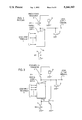
- This invention relates to dynamic logic gates.
- FIG. 1 shows a typical dynamic logic gate in which MOS transistors are used.
- element 1 is a logic output terminal
- element 2 is a capacitor
- element 3 is a precharging transistor
- element 4 are logic input terminals
- element 5 is a partial logic gate where the current between its two output terminals 5a and 5b is allowed to flow or is cut off according to the status of the logic inputs
- element 9 is a transistor that cuts off the current from the logic gate during the clock precharge period and conducts during other clock periods
- element 8 is a power supply.
- FIG. 2 shows the circuit of FIG. 1 with the partial logic gate 5 shown in more specific detail.
- elements 41-45 are logic input terminals for logic inputs D 1 -D 5 ;
- elements 51-55 are transistors composing the logic gate.
- a current can flow between the terminals 5a and 5b when the logic inputs D 1 -D 5 satisfy the following equation (1).
- the circuit of FIGS. 1 and 2 operates in the following sequence.
- the logic output generates normal values only when the clock ⁇ is a "1", at which time the logic output Q is expressed by the following equation (2).
- Dynamic logic gates such as these are frequently used because of the advantage that no steady-state operating current flows, but they are operated at low power and, as the number of inputs increases, the circuit does not become too complex; whereas, in the case of an ordinary CMOS static logic gate, the circuit becomes complex.
- the object of this invention is to produce dynamic logic gates which can be operated at a high speed.
- the dynamic logic gates of this invention include a logic output terminal, a capacitor connected to the logic output terminal, a precharge device that operates in synchronism with a clock and precharges the capacitor to a prescribed voltage level during one half of the clock cycle, a partial logic gate with at least one logic input terminal wherein the current between its two output terminals is allowed to flow or is cut off depending on the state of the at least one logic input and wherein one of these two output terminals is connected to the logic output terminal, a bipolar transistor whose emitter is grounded and whose collector is connected to the logic output terminal, and whose base is connected to the other of the two output terminals of the logic circuit, and a discharge device for discharging the charge stored in the base of the bipolar transistor.
- the current flowing to the partial logic gate becomes the base current of the bipolar transistor, and the bipolar transistor amplifies the current and rapidly discharges the charge on the capacitor using the amplified current, whereby the output terminal voltage rapidly trails off. Since the partial logic gate is connected between the base and collector of the bipolar transistor, when the collector voltage decreases, the current flowing to the base is reduced. When the voltage between the base and collector becomes zero, the base current is zero, and saturation of the bipolar transistor is prevented, which makes high-speed logic operations possible.
- FIG. 1 is a circuit diagram of a conventional dynamic logic gate.
- FIG. 2 is a more detailed circuit diagram of a conventional dynamic logic gate.
- FIG. 3 is a circuit diagram of a dynamic logic gate in accordance with a first embodiment of this invention.
- FIG. 4 is a more specific circuit diagram of the dynamic logic gate of FIG. 3.
- FIG. 5 is a circuit diagram of a conventional dynamic logic gate used for comparison with the first embodiment of this invention with respect to its effectiveness.
- FIG. 6 is a characteristic diagram comparing dependency of the delay time on the load capacity of the dynamic logic gate of the first embodiment of this invention with a gate of the conventional type.
- FIG. 7 is a circuit diagram of a dynamic logic gate in accordance with a second embodiment of this invention.
- FIG. 8 is a circuit diagram of a carry look ahead circuit in accordance with a third embodiment of this invention.
- FIG. 9 is a circuit diagram of a conventional carry look ahead circuit.
- FIG. 10 is a characteristic diagram comparing delay characteristics of the data for a carry look ahead circuit of the third embodiment of this invention with a conventional carry look ahead circuit obtained by using the channel widths of the constituent MOS transistors as a parameter.
- FIGS. 11-13 are circuit diagrams of modifications of the dynamic logic gate of FIG. 3.
- FIG. 3 shows first embodiment in accordance with this invention.
- element 1 is a logic output terminal
- element 2 is a capacitor
- element 3 is a precharging transitor
- element 4 are logic input terminals
- element 5 is a partial logic gate
- element 6 is a bipolar transistor
- element 7 is a transistor which operates as a discharge device for discharging the charge stored in the base of the bipolar transistor
- element 8 is a power supply.
- the transistors 3 and 7 are turned “on”.
- the transistor 6 is cut-off due to the low voltage between its base and its emitter, and no collector current flows. If the current flowing between the two terminals 5a and 5b of the partial logic gate 5 is either cut off are at a much lower value than the precharge current of the transistor 3, precharging occurs, and the capacitor 2 is charged and the logic output becomes a "1".
- the clock ⁇ is switched to a "1"
- the transistors 3 and 7 turn “off”, and if the two terminals 5a and 5b of the partial logic gate 5 are conducting current, the current flowing between the two terminals become the base current of the bipolar transistor 6, and the amplified base current becomes the collector current and rapidly discharges the capacitor 2.
- the capacitor 2 was not installed expressly, but it signifies an inherently formed capacitance, such as the parasitic capacitance of a transistor or a wiring capacitance.
- FIG. 4 the partial logic gate 5 as shown in FIG. 3 has been replaced by a specific MOS transistor 50.
- MOS transistor 50 In order to simplify the following explanation, one input and one transistor are used. Since the precharge operation time is the same, the time for the logic-generating period is compared.
- FIG. 5 a conventional circuit composed of MOS transistors alone is shown in FIG. 5, and the speed of this circuit is calculated.
- FIG. 5 when the capacitance of the capacitor 2 is C and the voltage of the power supply 8 is V CC , the voltage of the logic output terminal rises to V CC during the precharge period. If the clock ⁇ is switched in this state, the charge on capacitor 2 is discharged by the transistor 50, and a logic output is obtained. If we assume the logic threshold to be 1/2 V CC , the delay time t pd until a logic output is obtained is expressed by the following equation (3) denoting the discharge current as I d (t). ##EQU1##
- V CC is impressed between the gate and the source of the MOS transistor 50, and if we assume that this transistor operates in a saturation region, the discharge current I d (t) is expressed by the following equation (4). ##EQU2##
- ⁇ is a gain factor
- V gs is the voltage between the gate and the source
- V t is the threshold voltage of the transistor.
- the base current I B of the bipolar transistor 6 is equal to the current drain of the MOS transistor 50, and considering the fact that the source potential of this transistor is higher than the ground potential by the voltage V BE between the base and the emitter of the bipolar transistor 6, the delay time can be expressed by the following equation (6). ##EQU4##
- collector current I C can be approximated by the following equation (7). ##EQU5##
- Equation (9) that gives the delay time in this invention
- equation (5) that gives the delay time of a conventional circuit using a MOS transistor
- K shows how much greater acceleration has been achieved by the circuit as compared to a conventional circuit.
- ⁇ O is the carrier mobility
- C OX is the unit capacity of the gate
- W is the gate width
- L is the gate length
- FIG. 6 a simulation was performed using a computer. It shows the load capacity dependency of the delay times of this intention shown in FIG. 4 compared to the conventional case shown in FIG. 5.
- the delay time of this invention is lower than that of the conventional case; at a capacitance of 3 PF, if it about 1/8 that of the conventional case. Consequently, when this invention is used, not only is a sharp increase in speed accomplished by a slight increase in the circuit scale, but less speed degradation occurs as compared to a conventional circuit even when the transistor channel width is reduced. Therefore, it is very effective for the reduction of LSI chip area. This is very effective for he reduction of LSI chip area. This is an important feature of this invention, and it is made possible for the first time by the high-speed nature of a bipolar transistor.
- FIG. 7 is a dynamic logic gate of a second embodiment in accordance with this invention.
- a transistor 10 is installed between the partial logic gate 5 and the bipolar transistor base and is as a switching device used to cut off the current between the partial logic gate 5 and the bipolar transistor base during the precharge period of the clock and to conduct during other clock periods.
- the current flowing between the two terminals 5a and 5b becomes the base current of the bipolar transistor 6, and the amplified base current becomes the collector current and rapidly discharges the capacitor 2. Therefor, a logic output is generated at a high speed.
- FIG. 8 is a carry look ahead circuit, which is a third embodiment in accordance with this invention.
- a carry look ahead circuit is used in an adder-subtracter;
- FIG. 8 has a 4-bit configuration.
- the logic gate is built as a cascade connection.
- elements 60-68 satisfy the logic expression shown in equation (14).
- Transistors 11 and 12 composing the partial logic gate are transistors forming an inverter circuit installed to obtain positive logic outputs.
- the rest of the circuit of FIG. 8 is identical to the second embodiment in accordance with this invention as shown in FIG. 7.
- the transistors 3 and 7 turn “off", and the transistor 10 turns "on”. Therefore, when equation (14) is true, the base current of the transistor 6 flows, and the collector current of the transistor 6 rapidly removes out the precharged charge, thereby changing the inverter output C 4 to a "1".
- FIG. 9 shows a conventional carry look ahead circuit used for a performance evaluation of the third embodiment in accordance with this invention.
- the transistors 60-68 effecting equation (14) and the inverter circuit are identical to the third embodiment in accordance with this invention as shown in FIG. 8.
- FIG. 10 compares the delay time with respect to word length of the carry look ahead circuit of this invention as shown in FIG. 8 with the conventional carry look ahead circuit as shown in FIG. 9 using the channel width W of the transistors 60-68 as a parameter.
- the speed increase with approximately 4-fold, and even at a channel width of 10 ⁇ m, it was as high as 2.7-fold. Consequently, the carry look ahead circuit of this invention is designed for a sharp increase in speed as compared to a conventional circuit, and it also has the advantage of building higher density circuits since speed does not decrease markedly even when the channel width of the transistor is small.
- FIG. 11 shows a diagram of dynamic logical circuit of a precharge means in which the PMOS 3 own in FIG. 3 is replaced by a bipolar transistor 100.
- a precharge means consisting of the bipolar transistor 100 having a driving capability higher than that of the PMOS 3, a precharge at a speed substantially higher than that of the dynamic logical circuit shown in FIG. 3 can be realized.
- the precharge voltage at the logic output terminal 1 is lower by 0.7 volt than the source voltage which is 8 volts.
- the threshold voltage between gate and source of a PMOS transistor 105 having a CMOS gate formed by the PMOS transistor 105 and an NMOS transistor 106 becomes higher than the threshold voltage of the transistor 105, and this produces an unfavorable situation where the PMOS transistor 105 is not completely turned off, yielding a very high sustained through-current which brings its power consumption upward.
- FIG. 13 shows a diagram of a dynamic logic circuit in which the discharge means consisting of a discharge transistor 7 used to discharge the base charge of the bipolar transistor 6 shown in FIG. 3 to ground, is replaced by a discharge means consisting of a discharge transistor 7 connected to a second power supply 102 in addition to the modification of the above described precharge means.
- This discharge means is characterized by the setting of the second power supply voltage at about 0.5 volts, and the discharge of the base charge of the bipolar transistor 6 to the second power supply 102 through the discharge transistor 7.
- the bipolar transistor becomes conductive when the base-emitter voltage becomes more than 0.7 volts and becomes non-conductive (that is-in an OFF state) at a base voltage of less than 0.7 volts, an adequately stable OFF state can be attained when the power supply voltage is set at about 0.5 volts.
- the base-emitter capacitance has to be charged up to 0.7 volts starting from an initial voltage of 0.5 volts when the discharge means shown in FIG. 13 is employed. Therefore, signal generation at a higher speed becomes possible by employing this discharge means, and, by employing the discharge means shown in FIG. 13. the high speed of the dynamic logic gate which is a feature of this invention can be further utilized effectively.
- the precharge means encircled by a broken line in FIG. 11 can also be similarly applied to the embodiments of the present invention shown in FIGS. 3, 4, 7, and 8 respectively.
- this invention does not specify a logic format for the partial logic gate, it is possible to apply it to specific logic gates such as a half adder, full adder, or decoder circuit, etc. or to a general logic gate such as a logical sum or logical product device, etc. In all cases, it is possible to design higher speed, higher density, and smaller circuits, and it has considerable industrial application.
Abstract
A dynamic logic gate includes a precharge device for precharging the logic gate in synchronism with a clock; a partial logic gate arranged such that, depending on the logic states of the logic inputs, current is allowed to flow between its two terminals or is cut off; a bipolar transistor whose emitter is grounded, and a discharge device for discharging the charge stored in the base of the bipolar transistor during the precharge period. The logic gate speeds up the logic operation by suddenly discharging the load capacity of the circuitry by supplying the conducting current of the partial logic gate to the bipolar transistor base and using the high speed current amplification action of the bipolar transistor.
Description
This application is a continuation-in-part of U.S. application Ser. No. 07/324,038 filed Mar. 14, 1989.
This invention relates to dynamic logic gates.
FIG. 1 shows a typical dynamic logic gate in which MOS transistors are used.
In FIG. 1, element 1 is a logic output terminal; element 2 is a capacitor; element 3 is a precharging transistor; element 4 are logic input terminals; element 5 is a partial logic gate where the current between its two output terminals 5a and 5b is allowed to flow or is cut off according to the status of the logic inputs; element 9 is a transistor that cuts off the current from the logic gate during the clock precharge period and conducts during other clock periods, and element 8 is a power supply.
FIG. 2 shows the circuit of FIG. 1 with the partial logic gate 5 shown in more specific detail. In FIG. 2 elements 41-45 are logic input terminals for logic inputs D1 -D5 ; elements 51-55 are transistors composing the logic gate. A current can flow between the terminals 5a and 5b when the logic inputs D1 -D5 satisfy the following equation (1).
D.sub.1 ·D.sub.2 +D.sub.3 ·(D.sub.4 +D.sub.5)=1(1)
The circuit of FIGS. 1 and 2 operates in the following sequence. First, when the clock φ is a "0", the transistor 3 is "on", and the transistor 9 is "off". In this state, current flows from the power supply 8 to the capacitor 2 through transistor 3, and the capacitor 2 voltage rises, and the state of the logic output terminal 1 becomes "1" regardless of the state of the logic inputs D1 -D5. Next, as the clock phase changes and the clock φ becomes a "1", the transistor 3 turns "off", and the transistor 9 turns "on". In this state, if the two terminals 5a and 5b of the partial logic gate 5 are in a state which allows current to flow therebetween, the charge stored in the capacitor 2 is discharged through the two terminals 5a and 5b as well as transistor 9, and the state of the logic output terminal 1 becomes a "0". On the other hand, if the partial logic gate 5 is in a state such that the current between the two terminals 5a and 5b is cut off, a discharge path is not formed, and the state of the logic output terminal 1 remains a "1".
In other words, the logic output generates normal values only when the clock φ is a "1", at which time the logic output Q is expressed by the following equation (2).
Q=D.sub.1 ·D.sub.2 ·D.sub.3 ·(D.sub.4 +D.sub.5)(2)
Dynamic logic gates such as these are frequently used because of the advantage that no steady-state operating current flows, but they are operated at low power and, as the number of inputs increases, the circuit does not become too complex; whereas, in the case of an ordinary CMOS static logic gate, the circuit becomes complex.
However, there were shortcomings in that when the dynamic gates were used in a decoder or an ROM circuit, the capacitor 2 value reached several PF and the channel width was reduced in the partial logic gates. Consequently, the load driving capability decreased so as to increase the gate delay time.
The object of this invention is to produce dynamic logic gates which can be operated at a high speed.
In order to achieve the above object, the dynamic logic gates of this invention include a logic output terminal, a capacitor connected to the logic output terminal, a precharge device that operates in synchronism with a clock and precharges the capacitor to a prescribed voltage level during one half of the clock cycle, a partial logic gate with at least one logic input terminal wherein the current between its two output terminals is allowed to flow or is cut off depending on the state of the at least one logic input and wherein one of these two output terminals is connected to the logic output terminal, a bipolar transistor whose emitter is grounded and whose collector is connected to the logic output terminal, and whose base is connected to the other of the two output terminals of the logic circuit, and a discharge device for discharging the charge stored in the base of the bipolar transistor.
According to the above-mentioned configuration of this invention, the current flowing to the partial logic gate becomes the base current of the bipolar transistor, and the bipolar transistor amplifies the current and rapidly discharges the charge on the capacitor using the amplified current, whereby the output terminal voltage rapidly trails off. Since the partial logic gate is connected between the base and collector of the bipolar transistor, when the collector voltage decreases, the current flowing to the base is reduced. When the voltage between the base and collector becomes zero, the base current is zero, and saturation of the bipolar transistor is prevented, which makes high-speed logic operations possible.
FIG. 1 is a circuit diagram of a conventional dynamic logic gate.
FIG. 2 is a more detailed circuit diagram of a conventional dynamic logic gate.
FIG. 3 is a circuit diagram of a dynamic logic gate in accordance with a first embodiment of this invention.
FIG. 4 is a more specific circuit diagram of the dynamic logic gate of FIG. 3.
FIG. 5 is a circuit diagram of a conventional dynamic logic gate used for comparison with the first embodiment of this invention with respect to its effectiveness.
FIG. 6 is a characteristic diagram comparing dependency of the delay time on the load capacity of the dynamic logic gate of the first embodiment of this invention with a gate of the conventional type.
FIG. 7 is a circuit diagram of a dynamic logic gate in accordance with a second embodiment of this invention.
FIG. 8 is a circuit diagram of a carry look ahead circuit in accordance with a third embodiment of this invention.
FIG. 9 is a circuit diagram of a conventional carry look ahead circuit.
FIG. 10 is a characteristic diagram comparing delay characteristics of the data for a carry look ahead circuit of the third embodiment of this invention with a conventional carry look ahead circuit obtained by using the channel widths of the constituent MOS transistors as a parameter.
FIGS. 11-13 are circuit diagrams of modifications of the dynamic logic gate of FIG. 3.
FIG. 3 shows first embodiment in accordance with this invention. In FIG. 3 element 1 is a logic output terminal; element 2 is a capacitor; element 3 is a precharging transitor; element 4 are logic input terminals; element 5 is a partial logic gate; element 6 is a bipolar transistor; element 7 is a transistor which operates as a discharge device for discharging the charge stored in the base of the bipolar transistor, and element 8 is a power supply.
First, with the clock φ at "0", the transistors 3 and 7 are turned "on". The transistor 6 is cut-off due to the low voltage between its base and its emitter, and no collector current flows. If the current flowing between the two terminals 5a and 5b of the partial logic gate 5 is either cut off are at a much lower value than the precharge current of the transistor 3, precharging occurs, and the capacitor 2 is charged and the logic output becomes a "1". When the clock φ is switched to a "1", the transistors 3 and 7 turn "off", and if the two terminals 5a and 5b of the partial logic gate 5 are conducting current, the current flowing between the two terminals become the base current of the bipolar transistor 6, and the amplified base current becomes the collector current and rapidly discharges the capacitor 2. This is a salient feature of this invention and causes the logic output to be generated at a higher speed than is possible with a conventional type of gate. Incidentally, the capacitor 2 was not installed expressly, but it signifies an inherently formed capacitance, such as the parasitic capacitance of a transistor or a wiring capacitance.
Next, the speed improvement is shown more specifically. In FIG. 4, the partial logic gate 5 as shown in FIG. 3 has been replaced by a specific MOS transistor 50. In order to simplify the following explanation, one input and one transistor are used. Since the precharge operation time is the same, the time for the logic-generating period is compared. First, a conventional circuit composed of MOS transistors alone is shown in FIG. 5, and the speed of this circuit is calculated. In FIG. 5, when the capacitance of the capacitor 2 is C and the voltage of the power supply 8 is VCC, the voltage of the logic output terminal rises to VCC during the precharge period. If the clock φ is switched in this state, the charge on capacitor 2 is discharged by the transistor 50, and a logic output is obtained. If we assume the logic threshold to be 1/2 VCC, the delay time tpd until a logic output is obtained is expressed by the following equation (3) denoting the discharge current as Id (t). ##EQU1##
VCC is impressed between the gate and the source of the MOS transistor 50, and if we assume that this transistor operates in a saturation region, the discharge current Id (t) is expressed by the following equation (4). ##EQU2##
In equation (4), β is a gain factor, Vgs is the voltage between the gate and the source, and Vt is the threshold voltage of the transistor.
From equations (3) and (4), the delay time tpd is expressed by the following equation (5). ##EQU3##
Next, as for the delay time in the examples of this invention, the base current IB of the bipolar transistor 6 is equal to the current drain of the MOS transistor 50, and considering the fact that the source potential of this transistor is higher than the ground potential by the voltage VBE between the base and the emitter of the bipolar transistor 6, the delay time can be expressed by the following equation (6). ##EQU4##
In addition, the collector current IC can be approximated by the following equation (7). ##EQU5##
Where hFE is the current amplification, and fTi is the intrinsic cut-off frequency. Based on this, the following equation (8) will hold regarding the delay time tpd. ##EQU6##
In equation (8), if we assume ##EQU7## and approximate, tpd can be obtained from equation (5) shown by the following equation (9).
From equation (9) that gives the delay time in this invention and equation (5) that gives the delay time of a conventional circuit using a MOS transistor, we define a figure of merit K given by the following (10). K shows how much greater acceleration has been achieved by the circuit as compared to a conventional circuit. ##EQU8##
In addition, the gain factor β is expressed by the following equation (11). ##EQU9##
where μO is the carrier mobility, COX is the unit capacity of the gate, W is the gate width, and L is the gate length. Next, if we assume
V.sub.CC =5V, V.sub.BE =V.sub.T =0.8V, .sub.Ti =5G Hz, ##EQU10## equation (10) can be reduced to the following equation (12). ##EQU11##
Consequently, if the conditions of the following equation (13) holds, the delay time tpd of this invention would be smaller than that of a conventional circuit. ##EQU12## (C is in PF) If we assume W/L to be 10, the capacitance C is more than 20 PF, and the delay time is smaller in this invention than in the conventional case. This means that the delay time is usually smaller in this invention than the conventional case.
In FIG. 6, a simulation was performed using a computer. It shows the load capacity dependency of the delay times of this intention shown in FIG. 4 compared to the conventional case shown in FIG. 5. In most regions, the delay time of this invention is lower than that of the conventional case; at a capacitance of 3 PF, if it about 1/8 that of the conventional case. Consequently, when this invention is used, not only is a sharp increase in speed accomplished by a slight increase in the circuit scale, but less speed degradation occurs as compared to a conventional circuit even when the transistor channel width is reduced. Therefore, it is very effective for the reduction of LSI chip area. This is very effective for he reduction of LSI chip area. This is an important feature of this invention, and it is made possible for the first time by the high-speed nature of a bipolar transistor.
In addition, in the case of a circuit using bipolar transistors, the phenomenon of increased delay time is likely to occur due to transistor saturation. However, in the simulation, such a phenomenon does not occur. This is due to the fact that the MOS transistor 50 composing the partial logic gate 6 is connected to the bipolar transistor 6 between the base and the collector. When the collector voltage drops, the MOS transistor voltage between the drain and the source VDS drops, and the current flowing through the base decreases accordingly. When the voltage between the base and the collector becomes zero, the base current also becomes zero, and the collector-emitter voltage of the bipolar transistor 6 is maintained at about 0.6 V at a minimum. Consequently, saturation of the bipolar transistors 6 does not occur, and high-speed logic operation is possible.
FIG. 7 is a dynamic logic gate of a second embodiment in accordance with this invention. As opposed to the first example, a transistor 10 is installed between the partial logic gate 5 and the bipolar transistor base and is as a switching device used to cut off the current between the partial logic gate 5 and the bipolar transistor base during the precharge period of the clock and to conduct during other clock periods.
During the precharge period, since the clock φ becomes a "0" and the clock φ becomes a "1", the transistors 3 and 7 turn "on", and transistor 10 turns "off". Unlike the first example of this invention, it is not necessary to cut off the current flowing between the two terminals 5a and 5b of the partial logic gate 5 or to limit the current flowing to a value lower than the precharge current of the precharge transistor 3. An electric charge is stored in the capacitor 2 in this state, and the logic output becomes a "1". When the clock φ switches to a "1", the transistors 3 and 7 turn "off", and the transistor 10 turns "on". If the two terminals 5a and 5b of the partial logic gate 5 are conducting current, as in the first example of this invention, the current flowing between the two terminals 5a and 5b becomes the base current of the bipolar transistor 6, and the amplified base current becomes the collector current and rapidly discharges the capacitor 2. Therefor, a logic output is generated at a high speed.
FIG. 8 is a carry look ahead circuit, which is a third embodiment in accordance with this invention. A carry look ahead circuit is used in an adder-subtracter; FIG. 8 has a 4-bit configuration. The carry output C4 of this circuit can be expressed by a logic expression as shown in the following equation (14) by means of a carry generating input Gi (i=1-4), a carry propagating input Pi (i=1-4), and a carry signal from the previous step Co.
C.sub.4 =G.sub.4 +P.sub.4 ·(G.sub.3 +P.sub.3 ·(G.sub.2 +P.sub.2 ·(G.sub.1 +P.sub.1 ·C.sub.O))) (14)
In addition, when a multiple-bit configuration is used, the logic gate is built as a cascade connection. In the third example of this invention, elements 60-68 satisfy the logic expression shown in equation (14). Transistors 11 and 12 composing the partial logic gate are transistors forming an inverter circuit installed to obtain positive logic outputs. The rest of the circuit of FIG. 8 is identical to the second embodiment in accordance with this invention as shown in FIG. 7. During the precharge period with the clock pulse φ inverts to a "1", the transistors 3 and 7 turn "off", and the transistor 10 turns "on". Therefore, when equation (14) is true, the base current of the transistor 6 flows, and the collector current of the transistor 6 rapidly removes out the precharged charge, thereby changing the inverter output C4 to a "1".
FIG. 9 shows a conventional carry look ahead circuit used for a performance evaluation of the third embodiment in accordance with this invention. The transistors 60-68 effecting equation (14) and the inverter circuit are identical to the third embodiment in accordance with this invention as shown in FIG. 8.
FIG. 10 compares the delay time with respect to word length of the carry look ahead circuit of this invention as shown in FIG. 8 with the conventional carry look ahead circuit as shown in FIG. 9 using the channel width W of the transistors 60-68 as a parameter. At a channel length of 1.2 μm, the speed increase with approximately 4-fold, and even at a channel width of 10 μm, it was as high as 2.7-fold. Consequently, the carry look ahead circuit of this invention is designed for a sharp increase in speed as compared to a conventional circuit, and it also has the advantage of building higher density circuits since speed does not decrease markedly even when the channel width of the transistor is small.
FIG. 11 shows a diagram of dynamic logical circuit of a precharge means in which the PMOS 3 own in FIG. 3 is replaced by a bipolar transistor 100.
By employing a precharge means consisting of the bipolar transistor 100 having a driving capability higher than that of the PMOS 3, a precharge at a speed substantially higher than that of the dynamic logical circuit shown in FIG. 3 can be realized.
With this circuit construction, due to the presence of the base-emitter voltage which equals to approximately 0.7 volt, the precharge voltage at the logic output terminal 1 is lower by 0.7 volt than the source voltage which is 8 volts.
As a consequence of this, while the timing of the logic generation of the output signal is effected in a shorter period, the threshold voltage between gate and source of a PMOS transistor 105 having a CMOS gate formed by the PMOS transistor 105 and an NMOS transistor 106 becomes higher than the threshold voltage of the transistor 105, and this produces an unfavorable situation where the PMOS transistor 105 is not completely turned off, yielding a very high sustained through-current which brings its power consumption upward.
This drawback is eliminated by employing a precharge means shown in FIG. 12; that is, a precharging resistor is disposed between the base and emitter of precharging transistor 100 employed in the precharge means shown in FIG. 11.
By employing this circuit construction, when the precharge clock voltage rises to the voltage of the power supply 8, and the precharge voltage appearing at the logic output terminal 1 is lower than the power supply voltage by more than 0.7 volts, a high speed precharge similar to that of the precharge circuit shown in FIG. 11 can be obtained via the emitter current of the precharge transistor 100. Moreover, when the precharge voltage is lower than the power supply voltage by more than 0.7 volts, the precharge transistor 100 is brought into a cut-off condition, and the precharge voltage becomes equal to the power supply voltage by means of a current which passes through the precharge resistor 101 during a period of the precharge clock φ.
As described above, while a precharge which fully is swung to the supply voltage becomes possible by providing the precharging resistor 101, a high-speed precharge which is a principal advantage of the present invention without the conventional problem of precharge means shown in FIG. 11 can be accomplished.
FIG. 13 shows a diagram of a dynamic logic circuit in which the discharge means consisting of a discharge transistor 7 used to discharge the base charge of the bipolar transistor 6 shown in FIG. 3 to ground, is replaced by a discharge means consisting of a discharge transistor 7 connected to a second power supply 102 in addition to the modification of the above described precharge means. This discharge means is characterized by the setting of the second power supply voltage at about 0.5 volts, and the discharge of the base charge of the bipolar transistor 6 to the second power supply 102 through the discharge transistor 7.
Since the bipolar transistor becomes conductive when the base-emitter voltage becomes more than 0.7 volts and becomes non-conductive (that is-in an OFF state) at a base voltage of less than 0.7 volts, an adequately stable OFF state can be attained when the power supply voltage is set at about 0.5 volts.
When the clock φ becomes a low (L) level and the base current is injected into the base of transistor 6 from partial logic gate 5 according to the logic state of logic input terminal 4, a large collector current produced by the current amplification function of the bipolar transistor discharges the charge of the capacitor 2, and a logic output corresponding to the state of logic input terminal 4 is produced at the logic output terminal 1.
In the sequence shown above, by utilizing the discharge means of the present invention, signal generation at a speed higher than that obtained by the discharge means shown in FIG. 3 can be attained.
The reason for this is explained by the following. While the collector current of bipolar transistor 6 starts its flow if the base-emitter capacitance is charged by the current supplied from the partial logic gate 5 and the base-emitter voltage is brought to above 0.7 volts, the base-emitter capacitance has to be charged up to 0.7 volts starting from an initial voltage of 0 volt when the discharge means shown in FIG. 3 is employed.
However, the base-emitter capacitance has to be charged up to 0.7 volts starting from an initial voltage of 0.5 volts when the discharge means shown in FIG. 13 is employed. Therefore, signal generation at a higher speed becomes possible by employing this discharge means, and, by employing the discharge means shown in FIG. 13. the high speed of the dynamic logic gate which is a feature of this invention can be further utilized effectively.
Moreover, the precharge means encircled by a broken line in FIG. 11, the precharge means encircled by a broken line in FIG. 12, and the discharge means encircled by a broken line in FIG. 13 can also be similarly applied to the embodiments of the present invention shown in FIGS. 3, 4, 7, and 8 respectively.
As described above, it is possible, with this invention, to build a high-speed logic circuit in a simple configuration by directing the current that flows through the partial logic gate to the base of a bipolar transistor, and using the current amplifying action of the bipolar transistor to rapidly discharge the capacitor charge with the collector of the transistor. For example, if applied to the carry look ahead circuit, it is possible to design a logic gate with a 2.70- to 4-fold increase in speed compared with the conventional logic gate configured only with CMOS devices. In addition, even with a reduced channel width of the MOS transistors composing the partial logic gate, speed is compromised less in this invention than in a conventional circuit, which enables designing at higher density and miniaturizing the circuit. Furthermore, since this invention does not specify a logic format for the partial logic gate, it is possible to apply it to specific logic gates such as a half adder, full adder, or decoder circuit, etc. or to a general logic gate such as a logical sum or logical product device, etc. In all cases, it is possible to design higher speed, higher density, and smaller circuits, and it has considerable industrial application.
Claims (4)
1. A dynamic logic gate comprising:
a logic output terminal;
a capacitor connected to said logic output terminal;
a precharge means, comprising a bipolar transistor having a base connected to a clock for precharging and having an emitter connected to said capacitor and having a resistance means connected between said base and emitter of said bipolar transmitter and having a CMOS logic gate connected to said logic output terminal, for receiving and operating synchronously with said clock to precharge said capacitor to a prescribed voltage lever during a precharge period corresponding to one half cycle of said clock;
a partial logic gate having at least logic input terminal and first and second output terminals, wherein, depending on the logic state of said at least one logic input terminal, a current is allowed to flow between said first and second output terminals or is cut off, and wherein said first output terminal is connected to the said logic output terminal;
another bipolar transistor having an emitter which is grounded, and having a collector which is connected to said logic output terminal, and having a base which is connected to said second output terminal of said partial logic gate; and
a discharge means for discharging charge stored in said base of said another bipolar transistor during said precharge period of clock.
2. A dynamic logic gate comprising:
a logic output terminal;
a capacitor connected to said logic output terminal;
a precharge means, comprising a bipolar transistor having a base connected to a clock for precharging and having an emitter connected to said capacitor and having a resistor disposed between said base and emitter thereof and having a CMOS logic gate connected to said logic output terminal, for receiving and operating synchronously with said clock to precharge said capacitor to a prescribed voltage level during a precharge period corresponding to one half cycle of said clock;
a partial logic gate having at least one logic input terminal and first and second output terminals, wherein, depending on the logic state of said at least one logic input terminal, a current is allowed to flow between said first and second output terminals or is cut off, and wherein said first output terminal is connected to said logic output terminal;
another bipolar transistor having an emitter which is grounded and having a collector which is connected to said logic output terminal and having a base;
a switching means connected between said base and said second output terminal for cutting off the flow of current between said second output terminal and said base of said another bipolar transistor during said precharge period of said clock, and for allowing the flow of current during other periods of said clock; and
a discharging means comprising an MOS transistor for discharging charge stored in said base of said another bipolar transistor to a specified power supply having an output voltage on the order of 0.5 volts during said precharge period of said clock.
3. A dynamic logic gate comprising:
a logic output terminal;
a capacitor connected to said logic output terminal;
a precharge means for receiving and operating synchronously with a clock to precharge said capacitor to a prescribed voltage level during a precharge period corresponding to one half cycle of said clock;
a partial logic gate having at least logic input terminal and first and second output terminals, wherein, depending on the logic state of said at least one logic input terminal, a current is allowed to flow between said first and second output terminals or is cut off, and wherein said first output terminal is connected to the said logic output terminal;
a bipolar transistor having an emitter which is grounded, and having a collector which is connected to said logic output terminal, and having a base which is connected to said second output terminal of said partial logic gate; and
a discharging means comprising an MOS transistor for discharging change stored in said base of said bipolar transistor to a specified power supply having an output voltage on the order of 0.5 volts during said precharge period of said clock.
4. A dynamic logic gate comprising:
a logic output terminal;
a capacitor connected to said logic output terminal;
a precharge means, comprising a bipolar transistor having a base connected to a clock for precharging and having an emitter connected to said capacitor and having a resistor disposed between said base and emitter thereof and having a CMOS logic gate connected to said logic output terminal for receiving and operating synchronously with said clock to precharge said capacitor to a prescribed voltage level during a precharge period corresponding to one half cycle of said clock;
a partial logic gate having at least logic input terminal and first and second output terminals, wherein, depending on the logic state of said at least one logic input terminal, a current is allowed to flow between said first and second output terminals or is cut off, and wherein said first output terminal is connected to the said logic output terminal;
another bipolar transistor having an emitter which is grounded, and having a collector which is connected to said logic output terminal, and having a base which is connected to said second output terminal of said partial logic gate; and
a discharging means comprising an MOS transistor for discharging charge stored in said base of said another bipolar transistor to a specified power supply having an output voltage on the order of 0.5 volts during said precharge period of said clock.
Priority Applications (1)
| Application Number | Priority Date | Filing Date | Title |
|---|---|---|---|
| US07/631,283 US5144163A (en) | 1988-03-14 | 1990-02-20 | Dynamic BiCMOS logic gates |
Applications Claiming Priority (3)
| Application Number | Priority Date | Filing Date | Title |
|---|---|---|---|
| JP63-59719 | 1988-03-14 | ||
| JP63059719A JPH01232826A (en) | 1988-03-14 | 1988-03-14 | Dynamic type logic circuit |
| US07/631,283 US5144163A (en) | 1988-03-14 | 1990-02-20 | Dynamic BiCMOS logic gates |
Related Parent Applications (1)
| Application Number | Title | Priority Date | Filing Date |
|---|---|---|---|
| US07/324,038 Continuation-In-Part US5121002A (en) | 1988-03-14 | 1989-03-14 | Dynamic logic gates |
Publications (1)
| Publication Number | Publication Date |
|---|---|
| US5144163A true US5144163A (en) | 1992-09-01 |
Family
ID=26400791
Family Applications (1)
| Application Number | Title | Priority Date | Filing Date |
|---|---|---|---|
| US07/631,283 Expired - Fee Related US5144163A (en) | 1988-03-14 | 1990-02-20 | Dynamic BiCMOS logic gates |
Country Status (1)
| Country | Link |
|---|---|
| US (1) | US5144163A (en) |
Cited By (11)
| Publication number | Priority date | Publication date | Assignee | Title |
|---|---|---|---|---|
| US5506519A (en) * | 1994-06-03 | 1996-04-09 | At&T Corp. | Low energy differential logic gate circuitry having substantially invariant clock signal loading |
| US5514979A (en) * | 1994-11-28 | 1996-05-07 | Unisys Corporation | Methods and apparatus for dynamically reducing ringing of driver output signal |
| US5530380A (en) * | 1993-12-28 | 1996-06-25 | Nec Corporation | Decoder circuit which resists a fluctuation of a power supply |
| US5541536A (en) * | 1995-03-01 | 1996-07-30 | Sun Microsystems, Inc. | Rubberband logic |
| US5581497A (en) * | 1994-10-17 | 1996-12-03 | Intel Corporation | Carry skip adder with enhanced grouping scheme |
| US5619076A (en) * | 1994-12-19 | 1997-04-08 | General Signal Power Systems, Inc. | Method and apparatus for connection and disconnection of batteries to uninterruptible power systems and the like |
| US5623221A (en) * | 1992-02-28 | 1997-04-22 | Hitachi, Ltd. | Low noise MOSFET employing selective drive signals |
| US5642061A (en) * | 1995-04-17 | 1997-06-24 | Hitachi America, Ltd. | Short circuit current free dynamic logic clock timing |
| US5926038A (en) * | 1997-11-10 | 1999-07-20 | The United States Of America As Represented By The Secretary Of The Navy | Two-phase dynamic logic circuits for gallium arsenide complementary HIGFET fabrication |
| US6266800B1 (en) * | 1999-01-29 | 2001-07-24 | International Business Machines Corporation | System and method for eliminating effects of parasitic bipolar transistor action in dynamic logic using setup time determination |
| US6292029B1 (en) * | 1999-12-23 | 2001-09-18 | Intel Corporation | Method and apparatus for reducing soft errors in dynamic circuits |
Citations (5)
| Publication number | Priority date | Publication date | Assignee | Title |
|---|---|---|---|---|
| US4661723A (en) * | 1983-07-25 | 1987-04-28 | Hitachi, Ltd. | Composite circuit of bipolar transistors and field effect transistors |
| US4713796A (en) * | 1984-02-13 | 1987-12-15 | Hitachi, Ltd. | Semiconductor integrated circuit |
| US4740718A (en) * | 1986-04-26 | 1988-04-26 | Kabushiki Kaisha Toshiba | Bi-CMOS logic circuit |
| US4798981A (en) * | 1986-03-31 | 1989-01-17 | Kabushiki Kaisha Toshiba | Input circuit |
| US4849658A (en) * | 1986-08-08 | 1989-07-18 | Hitachi, Ltd. | Dynamic logic circuit including bipolar transistors and field-effect transistors |
-
1990
- 1990-02-20 US US07/631,283 patent/US5144163A/en not_active Expired - Fee Related
Patent Citations (6)
| Publication number | Priority date | Publication date | Assignee | Title |
|---|---|---|---|---|
| US4661723A (en) * | 1983-07-25 | 1987-04-28 | Hitachi, Ltd. | Composite circuit of bipolar transistors and field effect transistors |
| US4808850A (en) * | 1983-07-25 | 1989-02-28 | Hitachi, Ltd. | Composite circuit of bipolar transistors and field effect transistors |
| US4713796A (en) * | 1984-02-13 | 1987-12-15 | Hitachi, Ltd. | Semiconductor integrated circuit |
| US4798981A (en) * | 1986-03-31 | 1989-01-17 | Kabushiki Kaisha Toshiba | Input circuit |
| US4740718A (en) * | 1986-04-26 | 1988-04-26 | Kabushiki Kaisha Toshiba | Bi-CMOS logic circuit |
| US4849658A (en) * | 1986-08-08 | 1989-07-18 | Hitachi, Ltd. | Dynamic logic circuit including bipolar transistors and field-effect transistors |
Cited By (12)
| Publication number | Priority date | Publication date | Assignee | Title |
|---|---|---|---|---|
| US5623221A (en) * | 1992-02-28 | 1997-04-22 | Hitachi, Ltd. | Low noise MOSFET employing selective drive signals |
| US5530380A (en) * | 1993-12-28 | 1996-06-25 | Nec Corporation | Decoder circuit which resists a fluctuation of a power supply |
| US5506519A (en) * | 1994-06-03 | 1996-04-09 | At&T Corp. | Low energy differential logic gate circuitry having substantially invariant clock signal loading |
| US5581497A (en) * | 1994-10-17 | 1996-12-03 | Intel Corporation | Carry skip adder with enhanced grouping scheme |
| US5514979A (en) * | 1994-11-28 | 1996-05-07 | Unisys Corporation | Methods and apparatus for dynamically reducing ringing of driver output signal |
| US5619076A (en) * | 1994-12-19 | 1997-04-08 | General Signal Power Systems, Inc. | Method and apparatus for connection and disconnection of batteries to uninterruptible power systems and the like |
| US5541536A (en) * | 1995-03-01 | 1996-07-30 | Sun Microsystems, Inc. | Rubberband logic |
| US5642061A (en) * | 1995-04-17 | 1997-06-24 | Hitachi America, Ltd. | Short circuit current free dynamic logic clock timing |
| US5926038A (en) * | 1997-11-10 | 1999-07-20 | The United States Of America As Represented By The Secretary Of The Navy | Two-phase dynamic logic circuits for gallium arsenide complementary HIGFET fabrication |
| US6266800B1 (en) * | 1999-01-29 | 2001-07-24 | International Business Machines Corporation | System and method for eliminating effects of parasitic bipolar transistor action in dynamic logic using setup time determination |
| US6292029B1 (en) * | 1999-12-23 | 2001-09-18 | Intel Corporation | Method and apparatus for reducing soft errors in dynamic circuits |
| US6351151B2 (en) | 1999-12-23 | 2002-02-26 | Intel Corporation | Method and apparatus for reducing soft errors in dynamic circuits |
Similar Documents
| Publication | Publication Date | Title |
|---|---|---|
| JP2616142B2 (en) | Output circuit | |
| JP3801760B2 (en) | High voltage generation circuit for semiconductor devices | |
| US5144163A (en) | Dynamic BiCMOS logic gates | |
| US4593203A (en) | Semiconductor integrated circuit which allows adjustment of circuit characteristics in accordance with storage data of nonvolatile memory element | |
| JPS6129068B2 (en) | ||
| EP0346876B1 (en) | Semiconductor integrated circuit having a CMOS inverter | |
| US5663659A (en) | Semiconductor integrated circuit device comprising CMOS transistors and differentiator | |
| EP0361841B1 (en) | Bicmos logic circuit | |
| JP3513218B2 (en) | Interface circuit and voltage raising circuit comprising the same | |
| EP0069444B1 (en) | Trigger pulse generator | |
| US4352996A (en) | IGFET Clock generator circuit employing MOS boatstrap capacitive drive | |
| JPH0456400B2 (en) | ||
| US5121002A (en) | Dynamic logic gates | |
| KR930000821B1 (en) | Redundancy circuit for economizing electric power in memory particle | |
| JP2746117B2 (en) | Substrate bias circuit | |
| JPH0139244B2 (en) | ||
| KR20000022571A (en) | Rc delay time stabilization circuit | |
| JP2985564B2 (en) | Dynamic circuit | |
| JPH11312969A (en) | Semiconductor circuit | |
| JP2944277B2 (en) | Buffer circuit | |
| US5004938A (en) | MOS analog NOR amplifier and current source therefor | |
| JPH0777344B2 (en) | Output buffer circuit | |
| JP3226535B2 (en) | Output buffer circuit | |
| JPH0137008B2 (en) | ||
| JPH0616586B2 (en) | N OR circuit |
Legal Events
| Date | Code | Title | Description |
|---|---|---|---|
| AS | Assignment |
Owner name: MATSUSHITA ELECTRIC INDUSTRIAL CO., LTD., 1006 OAZ Free format text: ASSIGNMENT OF ASSIGNORS INTEREST.;ASSIGNORS:NAKASHIMA, SHOTA;YAMADA, HARUYASU;MATSUZAWA, AKIRA;REEL/FRAME:005622/0528;SIGNING DATES FROM 19910205 TO 19910208 |
|
| FEPP | Fee payment procedure |
Free format text: PAYOR NUMBER ASSIGNED (ORIGINAL EVENT CODE: ASPN); ENTITY STATUS OF PATENT OWNER: LARGE ENTITY |
|
| FPAY | Fee payment |
Year of fee payment: 4 |
|
| REMI | Maintenance fee reminder mailed | ||
| LAPS | Lapse for failure to pay maintenance fees | ||
| FP | Lapsed due to failure to pay maintenance fee |
Effective date: 20000901 |
|
| STCH | Information on status: patent discontinuation |
Free format text: PATENT EXPIRED DUE TO NONPAYMENT OF MAINTENANCE FEES UNDER 37 CFR 1.362 |