US5185754A - Spectrally stable laser diode with internal reflector - Google Patents
Spectrally stable laser diode with internal reflector Download PDFInfo
- Publication number
- US5185754A US5185754A US07/737,194 US73719491A US5185754A US 5185754 A US5185754 A US 5185754A US 73719491 A US73719491 A US 73719491A US 5185754 A US5185754 A US 5185754A
- Authority
- US
- United States
- Prior art keywords
- active region
- reflectors
- semiconductor body
- laser
- laser diode
- Prior art date
- Legal status (The legal status is an assumption and is not a legal conclusion. Google has not performed a legal analysis and makes no representation as to the accuracy of the status listed.)
- Expired - Lifetime
Links
Images


Classifications
-
- H—ELECTRICITY
- H01—ELECTRIC ELEMENTS
- H01S—DEVICES USING THE PROCESS OF LIGHT AMPLIFICATION BY STIMULATED EMISSION OF RADIATION [LASER] TO AMPLIFY OR GENERATE LIGHT; DEVICES USING STIMULATED EMISSION OF ELECTROMAGNETIC RADIATION IN WAVE RANGES OTHER THAN OPTICAL
- H01S5/00—Semiconductor lasers
- H01S5/10—Construction or shape of the optical resonator, e.g. extended or external cavity, coupled cavities, bent-guide, varying width, thickness or composition of the active region
- H01S5/1021—Coupled cavities
-
- H—ELECTRICITY
- H01—ELECTRIC ELEMENTS
- H01S—DEVICES USING THE PROCESS OF LIGHT AMPLIFICATION BY STIMULATED EMISSION OF RADIATION [LASER] TO AMPLIFY OR GENERATE LIGHT; DEVICES USING STIMULATED EMISSION OF ELECTROMAGNETIC RADIATION IN WAVE RANGES OTHER THAN OPTICAL
- H01S5/00—Semiconductor lasers
- H01S5/10—Construction or shape of the optical resonator, e.g. extended or external cavity, coupled cavities, bent-guide, varying width, thickness or composition of the active region
- H01S5/12—Construction or shape of the optical resonator, e.g. extended or external cavity, coupled cavities, bent-guide, varying width, thickness or composition of the active region the resonator having a periodic structure, e.g. in distributed feedback [DFB] lasers
-
- H—ELECTRICITY
- H01—ELECTRIC ELEMENTS
- H01S—DEVICES USING THE PROCESS OF LIGHT AMPLIFICATION BY STIMULATED EMISSION OF RADIATION [LASER] TO AMPLIFY OR GENERATE LIGHT; DEVICES USING STIMULATED EMISSION OF ELECTROMAGNETIC RADIATION IN WAVE RANGES OTHER THAN OPTICAL
- H01S5/00—Semiconductor lasers
- H01S5/06—Arrangements for controlling the laser output parameters, e.g. by operating on the active medium
- H01S5/062—Arrangements for controlling the laser output parameters, e.g. by operating on the active medium by varying the potential of the electrodes
- H01S5/06209—Arrangements for controlling the laser output parameters, e.g. by operating on the active medium by varying the potential of the electrodes in single-section lasers
- H01S5/06213—Amplitude modulation
-
- H—ELECTRICITY
- H01—ELECTRIC ELEMENTS
- H01S—DEVICES USING THE PROCESS OF LIGHT AMPLIFICATION BY STIMULATED EMISSION OF RADIATION [LASER] TO AMPLIFY OR GENERATE LIGHT; DEVICES USING STIMULATED EMISSION OF ELECTROMAGNETIC RADIATION IN WAVE RANGES OTHER THAN OPTICAL
- H01S5/00—Semiconductor lasers
- H01S5/10—Construction or shape of the optical resonator, e.g. extended or external cavity, coupled cavities, bent-guide, varying width, thickness or composition of the active region
- H01S5/16—Window-type lasers, i.e. with a region of non-absorbing material between the active region and the reflecting surface
Definitions
- the present invention relates to semiconductor diode lasers that have a construction designed to stabilize the output frequency of the emitted beam, and in particular to lasers characterized by their particular resonant cavity or having plural cavities.
- the possible spectral modes are dictated by the round trip resonances of the cavity. For typical laser geometrics, these resonances occur every 0.2 to 0.3 nanometers. Losses for adjacent spectral modes are very nearly equal. Therefore, though the laser oscillates in a single spectral mode while under steady state conditions, slight temperature or current variations can cause the laser to shift or "hop" to another spectral mode. Such mode hopping can be particularly pronounced when the laser is deliberately amplitude modulated as part of an optical communication system.
- Utaka et al. describe a semiconductor laser with five electrically isolated and independently driven regions to control the output characteristics of the laser.
- Three of the regions including an active filter region with a diffraction grating and two gain adjusting regions integrated on both sides of the active filter region, form a gain region.
- Two waveguide regions are disposed on each end of the gain region.
- Each region is independently driven to affect the refractive indices and gain of the regions, and thereby to control the oscillation wavelength of the laser.
- the transmission wavelength of the diffraction grating in the filter region substantially determines the wavelength that will be selected, while the current supplied to the gain adjusting regions largely determines the optical power output of the laser.
- Tokuda et al. describe a composite resonator-type semiconductor laser in which two independent laser portions of different cavity lengths are formed precisely and without cleavage by diffusing or implanting an impurity through a mask to mix a portion of the active region's quantum well structure or a superlattice structure of the optical waveguide at a precise location.
- the two laser portions are electrically isolated to obtain a tuning effect when one of the two laser portions is injected with a current that is less than a threshold value for laser oscillation.
- the mixed portion between the two laser portions is unpumped.
- the laser geometry may include a single internal reflector or have multiple internal reflectors forming an internal etalon.
- the geometry may combine such a reflector or reflectors with window regions at the laser facets.
- Grating feedback devices such as distributed feedback (DFB) or distributed Bragg reflector (DBR) structures may be combined with the internal reflector or reflectors.
- the current is independently controllable on the two sides of an internal reflector. This would add independent tunability of one cavity with respect to the other and lead to continuous wavelength tuning of the laser.
- the internal reflector structure may be formed in the laser diode by an impurity induced disordering (IID) technique. Internal reflection occurs due to the refractive index change in the higher aluminum content of disordered material. Incorporation of superlattice regions adjacent to the active region enhances the change produced by the disordering.
- IID impurity induced disordering
- Alternative processes for forming the internal reflector structure include etch and regrowth, ion implantation, laser disordering, diffusion and substrate etching prior to crystal growth.
- the internal mirror geometry has been demonstrated to provide a stable single spectral mode under current modulation.
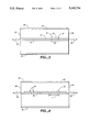
- FIG. 1 is a side view of a laser of the present invention having a single internal reflector.
- FIGS. 2a-2c are graphs of negative cavity loss versus frequency for the spectral modes of each of the two cavities formed by the internal reflector in the laser of FIG. 1, as well as of the resulting composite cavity of the laser of FIG. 1, respectively.
- FIGS. 3-6 are side views of alternate embodiments of lasers in accord with the present invention, respectively having two internal reflectors forming an active etalon, multiple periodic reflectors, an internal reflector combined with window regions and an internal reflector combined with a feedback grating.
- a laser diode 10 of the present invention includes an active region 12 and an optical waveguide 14 proximate to the active region 12 between cleaved mirror facets 16 and 18 of the diode body.
- the active region 12 may consist of either a single light emitting semiconductor layer or multiple layers in a quantum well structure. Cladding layers on both sides of the active region 12, having a higher electronic bandgap and lower refractive index than the active region 12, define the optical waveguide 14.
- the waveguide 14 may also be defined by a superlattice structure of multiple thin layers adjacent to the active region.
- Conductive contacts inject current into the active region to generate light by stimulated emission in the cavities between mirror facets 16 and 18.
- the light 22 may be emitted through either one or both facets 16 and 18.
- the waveguide 14 and active region 12 are partially interrupted at one point by an internal reflector 20.
- the internal reflector may be formed by selective impurity induced disordering of a local area of the waveguide 14. Diffusion of an impurity, such as zinc or silicon, through a region of the cladding or superstructure that forms part of the waveguide 14 locally alters the refractive index in that region creating a partially reflective interface for light propagating along the waveguide 14. A refractive index change of at least 0.02 compared to adjacent sections of the active region is preferred.
- the internal reflector may also be formed by etch and regrowth of wider bandgap GaAlAs, thereby creating a change in refractive index along the optical path. Other processes of forming the internal reflector include ion implantation, laser disordering, diffusion and substrate etching prior to crystal growth.
- the additional internal reflector 20 defines a first resonant optical cavity A between facet 16 and reflector 20 and a second resonant optical cavity B between reflector 20 and facet 18.
- FIG. 2A shows the negative cavity loss versus frequency of cavity A. The periodic nature of the resonant condition produces loss minima (peaks in the graph) separated by a frequency difference of c/2nL, where c is the speed of light in a vacuum, n is the effective refractive index of light in the waveguide 14 and L is the length of cavity A between facet 16 and reflector 20.
- FIG. 2B shows the corresponding resonance condition of cavity B. Note that the shorter length of cavity B produces a greater frequency separation between peaks of minimum loss.
- the internal reflector 20 within the semiconductor body is positioned at least 10% closer to one of the end facets 18 than to the other of the end facets 16.
- the resulting composite resonance condition is approximately the sum of the two conditions for cavities A and B, and is seen in FIG. 2C.
- the laser 10 has local loss minima, corresponding to cavity A, that define the possible longitudinal modes of the laser 10.
- the laser 10 with internal reflector 20 has adjacent modes, modes 26 and 27 for example, that have differing amounts of loss in the overall composite cavity.
- Absolute peaks of minimum loss, corresponding to the modes at points 26 and 28 in FIG. 2C are separated by a greater frequency, thereby minimizing mode hopping.
- the frequency separation of modes 26 and 28 is approximately c/2nl, where l is the length of cavity B.
- a laser diode 30 has an active region 32 and optical waveguide 34 proximate to the active region 32 between reflective facets 36 and 38. Conductive contacts 48 and 49 inject current into active region 32 to produce a light output 46 through one or both of the facets 36 and 38.
- the waveguide 34 is interrupted by a pair of internal reflectors 40 and 42 defining an etalon 44 between the reflectors 40 and 42. Typically, the internal reflectors 40 and 42 are spaced apart by about 3 to 20 ⁇ m. Except for the pair of reflectors 40 and 42 defining the etalon 44, the laser 30 is constructed in the same way as laser 10 in FIG. 1.
- the internal reflectors 40 and 42 themselves are also constructed in the same way as internal reflector 20 in FIG. 1, i.e. by local impurity induced disordering of the cladding layer or superlattice structure defining part of the waveguide 34.
- FIG. 3 there are effectively three cavities defined, respectively, between facet 36 and reflector 40, by etalon 44, and between reflector 42 and facet 38. If the two cavities other than etalon 44 have the same length, then the resonance condition is like that in FIG. 2C, with the size of the etalon 44 determining the spacing of absolute peaks of minimum cavity loss. It has been discovered that the multiple cavity effect on resonance condition works most effectively if etalon 44 is an active laser cavity. A passive etalon window does produce an additional cavity between its reflective boundaries, even if the boundaries are substantially spaced apart. However, the loss incurred in this design is substantial, because there is no gain in the window region of such an etalon. Thus, only discrete reflectors 40 and 42 separated by a gain section 45 produces an active etalon cavity 44 that reduces mode hopping.
- a laser diode 50 has an active region 52 and optical waveguide segments 54 spaced along the length of the active region 52 between reflective end facets 58 and 60.
- Conductive contacts 64 and 65 inject current into active region 52 to produce a light output 62 through one or both facets 58 and 60.
- internal reflectors 56 interrupt the waveguide 54 periodically, with an equal spacing between reflectors 56 or a period T of about 3 to 20 ⁇ m. The periodic reflections produce a cavity condition dominated by the period T rather than the facet-to-facet distance, so the resonant modes are spaced further apart at frequencies mc/2nT, where m is an integer.
- laser diodes 70 and 90 are substantially the same as laser diode 10 in FIG. 1, having active regions 72 and 92, waveguide 74 and 94 proximate to the active regions, end facets 76, 78 and 100, and conductive contacts 86, 87, 106 and 107 for current injection.
- the laser diodes produce light output 84 and 104 through one or both facets.
- internal reflectors 80 and 98 formed by impurity induced disordering (IID) produce a complex cavity condition that leads to reduced mode hopping under varying conditions.
- IID impurity induced disordering
- the embodiment in FIG. 5 also has window regions 82 and 83 formed adjacent to facets 76 and 78 respectively to reduce damage to the facets at high optical power levels.
- grating 96 is etched in a boundary surface of one of the cladding layers that make up waveguide 94.
- the current could be independently controlled on the two sides of the internal reflector, as shown, by having two electrically isolated conductive contacts 106 and 106' on one side of the laser diode body. This adds independent tunability of one cavity with respect to the other, and leads to continuous wavelength tunability of the laser 90.
- Other laser configurations in FIGS. 1-5 could also have independent current injection on different sides of one or more internal reflectors.
Abstract
Description
Claims (14)
Priority Applications (1)
| Application Number | Priority Date | Filing Date | Title |
|---|---|---|---|
| US07/737,194 US5185754A (en) | 1991-07-29 | 1991-07-29 | Spectrally stable laser diode with internal reflector |
Applications Claiming Priority (1)
| Application Number | Priority Date | Filing Date | Title |
|---|---|---|---|
| US07/737,194 US5185754A (en) | 1991-07-29 | 1991-07-29 | Spectrally stable laser diode with internal reflector |
Publications (1)
| Publication Number | Publication Date |
|---|---|
| US5185754A true US5185754A (en) | 1993-02-09 |
Family
ID=24962951
Family Applications (1)
| Application Number | Title | Priority Date | Filing Date |
|---|---|---|---|
| US07/737,194 Expired - Lifetime US5185754A (en) | 1991-07-29 | 1991-07-29 | Spectrally stable laser diode with internal reflector |
Country Status (1)
| Country | Link |
|---|---|
| US (1) | US5185754A (en) |
Cited By (10)
| Publication number | Priority date | Publication date | Assignee | Title |
|---|---|---|---|---|
| WO1994006181A1 (en) * | 1992-09-10 | 1994-03-17 | Bell Communications Research, Inc. | Multi-stripe array grating integrated cavity laser |
| US5600743A (en) * | 1994-08-31 | 1997-02-04 | Deutsche Telekom Ag | Optoelectronic multi-wavelength component |
| US5629954A (en) * | 1994-10-25 | 1997-05-13 | Trw Inc. | Semiconductor laser diode with integrated etalon |
| US5914977A (en) * | 1996-10-17 | 1999-06-22 | The Furukawa Electric Co., Ltd. | Semiconductor laser having a high-reflectivity reflector on the laser facets thereof, an optical integrated device provided with the semiconductor laser, and a manufacturing method therefor |
| US6122299A (en) * | 1997-12-31 | 2000-09-19 | Sdl, Inc. | Angled distributed reflector optical device with enhanced light confinement |
| US20030206267A1 (en) * | 2000-07-25 | 2003-11-06 | John Noto | Optical multiplexer and cross-switch using etched liquid crystal Fabry-Perot etalons |
| US6647046B1 (en) | 1999-11-23 | 2003-11-11 | Corning Lasertron, Inc. | Mode-selective facet layer for pump laser |
| US20060187995A1 (en) * | 2005-02-24 | 2006-08-24 | Jds Uniphase Corporation | Low loss grating for high efficiency wavelength stabilized high power lasers |
| US20080253421A1 (en) * | 2004-01-20 | 2008-10-16 | Greg Charache | High-Power Semiconductor Laser |
| US20210184427A1 (en) * | 2018-05-30 | 2021-06-17 | Nippon Telegraph And Telephone Corporation | Semiconductor Laser |
Citations (11)
| Publication number | Priority date | Publication date | Assignee | Title |
|---|---|---|---|---|
| US4680769A (en) * | 1984-11-21 | 1987-07-14 | Bell Communications Research, Inc. | Broadband laser amplifier structure |
| US4755015A (en) * | 1985-07-12 | 1988-07-05 | Matsushita Electric Industrial Co., Ltd. | Monolithic integrated semiconductor device of semiconductor laser and optical waveguide |
| US4788689A (en) * | 1985-02-26 | 1988-11-29 | Mitsubishi Denki Kabushiki Kaisha | Composite resonator-type semiconductor laser device |
| US4802182A (en) * | 1987-11-05 | 1989-01-31 | Xerox Corporation | Monolithic two dimensional waveguide coupled cavity laser/modulator |
| US4815084A (en) * | 1987-05-20 | 1989-03-21 | Spectra Diode Laboratories, Inc. | Semiconductor laser with integrated optical elements |
| US4829535A (en) * | 1987-10-28 | 1989-05-09 | Kokusai Denshin Denwa Kabushiki Kaisha | Variable wavelength semiconductor laser |
| US4853108A (en) * | 1987-06-29 | 1989-08-01 | Shell Oil Company | Process for hydrotreating hydrocarbon feeds |
| US4899361A (en) * | 1987-04-14 | 1990-02-06 | Nec Corporation | Optical filter device |
| US4960730A (en) * | 1987-07-16 | 1990-10-02 | Mitsubishi Denki Kabushiki Kaisha | Method of making a semiconductor light emitting device using out-diffusion from a buried stripe |
| US4977567A (en) * | 1988-10-28 | 1990-12-11 | Siemens Aktiengesellschaft | Semiconductor laser arrangement for high output powers in the lateral fundamental mode |
| US5031188A (en) * | 1990-04-30 | 1991-07-09 | At&T Bell Laboratories | Inline diplex lightwave transceiver |
-
1991
- 1991-07-29 US US07/737,194 patent/US5185754A/en not_active Expired - Lifetime
Patent Citations (11)
| Publication number | Priority date | Publication date | Assignee | Title |
|---|---|---|---|---|
| US4680769A (en) * | 1984-11-21 | 1987-07-14 | Bell Communications Research, Inc. | Broadband laser amplifier structure |
| US4788689A (en) * | 1985-02-26 | 1988-11-29 | Mitsubishi Denki Kabushiki Kaisha | Composite resonator-type semiconductor laser device |
| US4755015A (en) * | 1985-07-12 | 1988-07-05 | Matsushita Electric Industrial Co., Ltd. | Monolithic integrated semiconductor device of semiconductor laser and optical waveguide |
| US4899361A (en) * | 1987-04-14 | 1990-02-06 | Nec Corporation | Optical filter device |
| US4815084A (en) * | 1987-05-20 | 1989-03-21 | Spectra Diode Laboratories, Inc. | Semiconductor laser with integrated optical elements |
| US4853108A (en) * | 1987-06-29 | 1989-08-01 | Shell Oil Company | Process for hydrotreating hydrocarbon feeds |
| US4960730A (en) * | 1987-07-16 | 1990-10-02 | Mitsubishi Denki Kabushiki Kaisha | Method of making a semiconductor light emitting device using out-diffusion from a buried stripe |
| US4829535A (en) * | 1987-10-28 | 1989-05-09 | Kokusai Denshin Denwa Kabushiki Kaisha | Variable wavelength semiconductor laser |
| US4802182A (en) * | 1987-11-05 | 1989-01-31 | Xerox Corporation | Monolithic two dimensional waveguide coupled cavity laser/modulator |
| US4977567A (en) * | 1988-10-28 | 1990-12-11 | Siemens Aktiengesellschaft | Semiconductor laser arrangement for high output powers in the lateral fundamental mode |
| US5031188A (en) * | 1990-04-30 | 1991-07-09 | At&T Bell Laboratories | Inline diplex lightwave transceiver |
Cited By (18)
| Publication number | Priority date | Publication date | Assignee | Title |
|---|---|---|---|---|
| US5351262A (en) * | 1992-09-10 | 1994-09-27 | Bell Communications Research, Inc. | Multi-stripe array grating integrated cavity laser |
| WO1994006181A1 (en) * | 1992-09-10 | 1994-03-17 | Bell Communications Research, Inc. | Multi-stripe array grating integrated cavity laser |
| US5600743A (en) * | 1994-08-31 | 1997-02-04 | Deutsche Telekom Ag | Optoelectronic multi-wavelength component |
| US5629954A (en) * | 1994-10-25 | 1997-05-13 | Trw Inc. | Semiconductor laser diode with integrated etalon |
| US5914977A (en) * | 1996-10-17 | 1999-06-22 | The Furukawa Electric Co., Ltd. | Semiconductor laser having a high-reflectivity reflector on the laser facets thereof, an optical integrated device provided with the semiconductor laser, and a manufacturing method therefor |
| US6122299A (en) * | 1997-12-31 | 2000-09-19 | Sdl, Inc. | Angled distributed reflector optical device with enhanced light confinement |
| US6647046B1 (en) | 1999-11-23 | 2003-11-11 | Corning Lasertron, Inc. | Mode-selective facet layer for pump laser |
| US20030214622A1 (en) * | 2000-07-25 | 2003-11-20 | John Noto | Optical multiplexer and cross-switch using etched liquid crystal Fabry-Perot etalons |
| US20030206267A1 (en) * | 2000-07-25 | 2003-11-06 | John Noto | Optical multiplexer and cross-switch using etched liquid crystal Fabry-Perot etalons |
| US6757046B2 (en) | 2000-07-25 | 2004-06-29 | Scientific Solutions, Inc. | Optical multiplexer and cross-switch using etched liquid crystal Fabry-Perot etalons |
| US6812993B2 (en) | 2000-07-25 | 2004-11-02 | Scientific Solutions, Inc. | Optical multiplexer and cross-switch using etched liquid crystal fabry-perot etalons having enhanced spectral resolution and transmission characteristic |
| US6954253B2 (en) | 2000-07-25 | 2005-10-11 | Scientific Solutions, Inc. | Optical multiplexer and cross-switch using etched liquid crystal fabry-perot etalons |
| US20080253421A1 (en) * | 2004-01-20 | 2008-10-16 | Greg Charache | High-Power Semiconductor Laser |
| US7889776B2 (en) | 2004-01-20 | 2011-02-15 | Trumpf Photonics Inc. | High-power semiconductor laser |
| US20060187995A1 (en) * | 2005-02-24 | 2006-08-24 | Jds Uniphase Corporation | Low loss grating for high efficiency wavelength stabilized high power lasers |
| US7457341B2 (en) | 2005-02-24 | 2008-11-25 | Jds Uniphase Corporation | Low loss grating for high efficiency wavelength stabilized high power lasers |
| US20210184427A1 (en) * | 2018-05-30 | 2021-06-17 | Nippon Telegraph And Telephone Corporation | Semiconductor Laser |
| US11557876B2 (en) * | 2018-05-30 | 2023-01-17 | Nippon Telegraph And Telephone Corporation | Semiconductor laser |
Similar Documents
| Publication | Publication Date | Title |
|---|---|---|
| US5398256A (en) | Interferometric ring lasers and optical devices | |
| EP0169567B1 (en) | Semiconductor laser device | |
| US5327448A (en) | Semiconductor devices and techniques for controlled optical confinement | |
| EP0314490B1 (en) | Semiconductor laser | |
| EP0300790B1 (en) | Semiconductor laser | |
| US6687267B2 (en) | Widely tunable laser | |
| US5185754A (en) | Spectrally stable laser diode with internal reflector | |
| US5805627A (en) | Laser diode and optical communications system using such laser diode | |
| US20020141467A1 (en) | Semiconductor laser device | |
| US6810067B2 (en) | Single mode grating-outcoupled surface emitting laser with broadband and narrow-band DBR reflectors | |
| US6888874B2 (en) | Single-wavelength, unequal-length-multi-cavity grating-outcoupled surface emitting laser with staggered tuned distributed Bragg reflectors | |
| US5528616A (en) | Asymmetric dual waveguide laser | |
| US5953358A (en) | Semiconductor laser device | |
| EP0194894A2 (en) | A semiconductor laser | |
| US4773077A (en) | Internal reflection interferometric semiconductor laser apparatus | |
| JP3382471B2 (en) | Semiconductor optical device and optical network using the same | |
| JPH0479287A (en) | Wavelength variable semiconductor laser | |
| WO2021148120A1 (en) | Single-mode dfb laser | |
| JPS63228795A (en) | Distributed feedback type semiconductor laser | |
| US20240113504A1 (en) | Extended-cavity diode laser component and method for producing same | |
| US20030099268A1 (en) | Laser device and methods of making and using same | |
| WO2023227189A1 (en) | Tilted semiconductor laser | |
| JPH08274412A (en) | Polarization modulation semiconductor laser and its driving method | |
| JP4985368B2 (en) | Semiconductor laser device | |
| JPS59152685A (en) | Semiconductor laser element |
Legal Events
| Date | Code | Title | Description |
|---|---|---|---|
| AS | Assignment |
Owner name: SPECTRA DIODE LABORATORIES, INC. A CORPORATION Free format text: ASSIGNMENT OF ASSIGNORS INTEREST.;ASSIGNORS:CRAIG, RICHARD R.;WELCH, DAVID F.;ZUCKER, ERIK P.;AND OTHERS;REEL/FRAME:005799/0636 Effective date: 19910729 |
|
| AS | Assignment |
Owner name: FIRST NATIONAL BANK OF BOSTON, THE Free format text: ASSIGNMENT OF ASSIGNORS INTEREST.;ASSIGNOR:SPECTRA DIODE LABORATORIES, INC.;REEL/FRAME:006187/0189 Effective date: 19920715 |
|
| STCF | Information on status: patent grant |
Free format text: PATENTED CASE |
|
| AS | Assignment |
Owner name: SDL, INC., CALIFORNIA Free format text: MERGER;ASSIGNOR:SPECTRA DIODE LABORATORIES, INC.;REEL/FRAME:006545/0782 Effective date: 19930312 |
|
| FEPP | Fee payment procedure |
Free format text: PAYOR NUMBER ASSIGNED (ORIGINAL EVENT CODE: ASPN); ENTITY STATUS OF PATENT OWNER: LARGE ENTITY |
|
| FPAY | Fee payment |
Year of fee payment: 4 |
|
| FEPP | Fee payment procedure |
Free format text: PAYOR NUMBER ASSIGNED (ORIGINAL EVENT CODE: ASPN); ENTITY STATUS OF PATENT OWNER: LARGE ENTITY Free format text: PAYER NUMBER DE-ASSIGNED (ORIGINAL EVENT CODE: RMPN); ENTITY STATUS OF PATENT OWNER: LARGE ENTITY |
|
| AS | Assignment |
Owner name: SDL, INC., CALIFORNIA Free format text: ASSIGNMENT OF ASSIGNORS INTEREST;ASSIGNOR:FLEET NATIONAL BANK (FORMERLY KNOWN AS THE FIRST NATIONAL BANK OF BOSTON);REEL/FRAME:010958/0310 Effective date: 20000512 |
|
| FPAY | Fee payment |
Year of fee payment: 8 |
|
| AS | Assignment |
Owner name: JDS UNIPHASE CORPORATION, CALIFORNIA Free format text: ASSIGNMENT OF ASSIGNORS INTEREST;ASSIGNOR:SDL, INC.;REEL/FRAME:013269/0920 Effective date: 20020815 |
|
| FPAY | Fee payment |
Year of fee payment: 12 |
|
| FEPP | Fee payment procedure |
Free format text: PAYER NUMBER DE-ASSIGNED (ORIGINAL EVENT CODE: RMPN); ENTITY STATUS OF PATENT OWNER: LARGE ENTITY Free format text: PAYOR NUMBER ASSIGNED (ORIGINAL EVENT CODE: ASPN); ENTITY STATUS OF PATENT OWNER: LARGE ENTITY |